Formation of Palladium Silicide on Heavily Doped Si(001) Substrates
Using Ti Intermediate Layer
Risa Suryana
, Osamu Nakatsuka, and Shigeaki Zaima
Department of Crystalline Materials Science, Graduate School of Engineering, Nagoya University, Furo-cho, Chikusa-ku, Nagoya 464-8603, Japan
Received October 31, 2009; revised January 19, 2010; accepted January 21, 2010; published online May 20, 2010
The formation of palladium silicide on Pd/Ti/Si systems with and without heavy B-doping has been investigated. For comparison, Pd2Si was also formed on Pd/Si systems. The agglomeration of Pd2Si could be retarded in Pd/Ti/Si systems with and without B-doping after annealing at 600C. The existence of the Ti layer could improve the thermal stability of Pd
2Si. In addition, epitaxial or highly oriented Pd2Si formed in Pd/Ti/Si systems. The two orientation relationships of Pd2Si layers were identified to be Pd2Si½1 110 kSi½1101 and Pd2Si½110 kSi½001, and Pd2Si½100 kSi½1110 andPd2Si½001 kSi½001. The formation of strained epitaxial Pd2Si layers was found in Pd/Ti/Si systems. The improvement in the thermal stability of Pd2Si and the formation of epitaxial or highly oriented Pd2Si in Pd/Ti/Si systems were observed with and without B-doping. #2010 The Japan Society of Applied Physics
DOI:10.1143/JJAP.49.05FA09
1. Introduction
Metal silicides have been fascinating materials owing to their technological application as ohmic contacts, metal gates, Schottky contacts, and interconnects. Palladium (Pd) silicide is potentially attractive from the viewpoint of contact materials for shallow junctions because Pd forms a
metal-rich silicide, Pd2Si,1)which remains stable up to 700C after
formation at a low temperature, and the consumption of Si
for Pd2Si formation is smaller than those of NiSi, NiSi2,
CoSi2 and TiSi2. In addition, Pd2Si has a low Schottky
barrier height for a p-type contact (0:3eV).2)However, the
agglomeration of Pd2Si has been a serious problem that
results in the degradation of metal contact (source/drain)
performance in metal–oxide–semiconductor field-effect
transistor (MOSFET) applications. We previously reported
that Pd2Si agglomeration occurs at a temperature of 550C
in Pd/Si systems.3)
Epitaxial or highly oriented silicides on Si substrates have many advantages over polycrystalline silicides, such as a high thermal robustness, an improved Schottky barrier uniformity, a reduced junction shorting, and a suppressed dopant redistribution after the formation of contacts on shallow junctions. The epitaxial growth of metal silicides could be induced through either the implantation of an impurity into a Si substrate prior to metal deposition or using a metal intermediate layer between a metal film and a Si
substrate. For example, the presence of BF2, B, and F atoms
was found to promote the epitaxial growth of NiSi2 in Ni
thin films on Si substrates at low temperatures.4,5)
Previous-ly, we reported that the formation of an epitaxial NiSi2layer
at low temperatures was due to a titanium intermediate layer
in Ni/Ti/Si systems.6,7)Most papers indicated that the Pd2Si
films grown on Si(111) showed a strong tendency toward an epitaxial single-crystal growth, while on other Si
orienta-tions, the azimuth orientation of Pd2Si was completely
random.8,9)It has been reported that epitaxial Pd
2Si could be
formed on Si(001) using a Ti intermediate layer.10,11)
However, there is no data on palladium silicide formation by using a Ti layer on heavily doped Si(001). As a thin silicide layer on a heavily doped junction is important for forming a shallow junction, it is necessary to clarify
properties of Pd silicide thin layers for the contact application of Si MOSFETs. In this study, we investigated the growth and thermal stability of Pd silicide thin films on heavily B-doped Si(001) using a Ti intermediate layer.
2. Experimental Methods
The substrates used were n-type Si(001) with a resistivity of
0.1–10cm. After standard acid treatment, the wafers were
dipped into a diluted HF solution and rinsed for 5 s in deionized water in order to remove the surface oxide and to
obtain H-passivated surfaces.12) Immediately, some wafers
were loaded into the oxidation chamber at 1000C for 2 h in
order to obtain a SiO2 thickness of 50 nm. Then, the ion
implantation of B was performed using a BF3 source with
doses of31014 and11015cm2
at an energy of 30 kV. After the ion implantation, a rapid thermal annealing (RTA)
at 1100C for 30 s was performed to realize
recrystalliza-tion. Again, the wafers were chemically cleaned as men-tioned above, while the other wafers were loaded into the vacuum chamber without ion implantation.
A 10-nm-thick Pd layer or a 2-nm-thick Ti layer followed by a 10-nm-thick Pd layer was formed on the substrate by electron gun evaporation in an ultrahigh-vacuum chamber
whose base pressure was below 1106
Pa. Hereafter, these samples were called Pd/Si or Pd/Ti/Si samples, respectively. The samples were successively annealed at
300C in the same chamber for 10 min, and then, they were
exposed to atmospheric conditions. Some samples were additionally annealed at temperatures ranging from 400 to
600C for 30 s in N
2 ambient using an RTA system. X-ray
diffraction (XRD) analysis using a Cu K source,
cross-sectional transmission electron microscopy (XTEM), and scanning electron microscopy (SEM) were carried out to reveal the crystalline structures and morphology of the films. The sheet resistance of the films was measured by a linear four-point probe method.
3. Results and Discussion
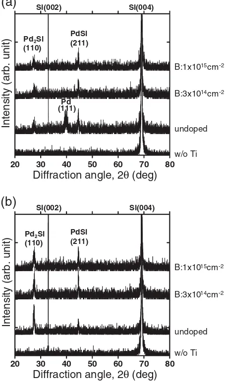
Figure 1 shows the X-ray diffraction (XRD)2=!spectra of
Pd/Si and Pd/Ti/Si samples with and without B-doping
after annealing at 300C for 10 min and additional RTA at
600C for 30 s. Two diffraction peaks at about 27.45 and
44.36 are identified as Pd
2Si 110 and PdSi 211,
respec-tively. These peaks also appear on Pd/Ti/Si samples with
and without B-doping at 400 – 500C but not on the samples
without a Ti layer (not shown). To increase the sensitivity for identifying the silicide phase and to determine whether the silicide film has a polycrystalline or highly oriented
structure, the grazing-angle XRD2was used. The
grazing-angle XRD2spectra clearly confirmed that polycrystalline
Pd2Si was predominantly formed in Pd/Si at 300C, as
shown in Fig. 2. In contrast, in Pd/Ti/Si samples with and
without B-doping, diffraction peaks of Pd2Si are very weak
after annealing at 300C. These results indicate the
formation of epitaxial or highly oriented Pd2Si in Pd/Ti/Si
systems with and without B-doping at low and high doses of B atoms. It is considered that a Ti intermediate layer plays a role larger than that of a B impurity in the formation of
epitaxial or highly oriented Pd2Si.
The dependence of crystalline orientation on annealing temperature is shown in Fig. 3. Normalized intensity is obtained from all intensities in Fig. 1, which were normal-ized by the intensity of Si substrates and the powder
diffraction intensity ratio of Pd2Si 110 and PdSi 211 planes.
The intensities of Pd2Si 110 increase with annealing
20 30 40 50 60 70 80
Intensity (arb. unit)
Diffraction angle, 2
θ
(deg)
Si(002) Si(004)
Diffraction angle, 2
θ
(deg)
Si(002) Si(004) interlayer, the Pd (10 nm)/Ti (2 nm)/Si system without B-doping, and the Pd (10 nm)/Ti (2 nm)/Si systems with B-doping at31014
Diffraction angle, 2
θ
(deg)
Intensity (arb. unit)
Ti interlayer, and with and without B-doping at31014and11015 cm2after annealing at 300C.
250 300 350 400 450 500 550 600 650
(a)
B :1x1015 cm-2
Annealing temperature (°C)
Normalized intensity (arb. unit)
B :3x1014cm-2 undoped
250 300 350 400 450 500 550 600 650
(b)
Annealing temperature (°C) B :1x1015 cm-2
B :3x1014cm-2 undoped
Normalized intensity (arb. unit)
Fig. 3. Normalized intensities of (a) Pd2Si 110 and (b) PdSi 211 after annealing from 300 to 600C in Pd (10 nm)/Ti (2 nm)/Si systems without
temperature, while those of PdSi 211 remain almost constant. If it is considered that the intensity is directly proportional to the volume of silicide domains, the volume
of Pd2Si domain increases with annealing temperature, while
the volume of PdSi domain remains almost constant. These
results indicate that Pd2Si and PdSi are formed during the
first-step annealing at 300C and we suggest that the growth
rate of Pd2Si is markedly higher than that of PdSi as
annealing temperature increases during the second-step RTA.
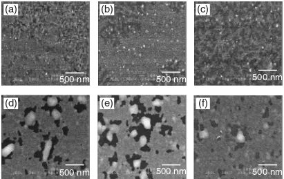
Figures 4(a)–4(c) and 4(d)–4(f) show SEM images of the Pd/Ti/Si and Pd/Si samples, respectively, with and without
B-doping after annealing at 600C for 30 s. The
agglomer-ation of Pd silicides (Pd2Si and PdSi) and the Si exposed
area corresponding to dark regions are clearly observed in the samples without a Ti intermediate layer. On the other hand, Si exposed regions hardly appear in the samples with a Ti intermediate layer. Figures 5(a)–5(c) show cross-sec-tional TEM images of the following samples after annealing
at 600C: the Pd/Si sample (a), the Pd/Ti/Si sample
without doping (b), and the Pd/Ti/Si sample with B-doping
at 11015cm2
(c). Some polycrystalline Pd2Si layers
consisting of pyramidal domains with wedge-shape facets are clearly observed in Fig. 5(a). The angle of the pyramidal
domains is estimated to be about 120, indicating that the
facets are Pd2Si 100 planes. On the other hand, the flatnesses
of the Pd2Si/Si interface are almost similar in the
Pd/Ti/Si-undoped and Pd/Ti/Si-B-doped samples. Considering that the dominant diffusion species during the formation of
Pd and Ti silicides are Pd and Si, respectively,13,14) it is
considered that, during annealing for silicidation, Pd atoms should diffuse into the Si substrate through a Ti intermediate
layer to form epitaxial Pd2Si, and Si atoms should diffuse
upward to form Ti silicides. Finally, it is considered that the stacked layer structure consisting of a Ti silicide surface
layer and a Pd2Si layer on a Si substrate is formed.
Here, we deduced the model of the dependence of interfacial reactions on annealing conditions. In general,
Pd2Si is formed by a diffusion-controlled process at
temper-atures ranging between 100 and 700C.8) In the case of
annealing at a temperature of as low as 600C in Pd/Si
systems, Pd atoms directly diffuse through Si and the Pd2Si
domain rapidly grows. As a result, pyramidal Pd2Si domains
are individually formed with large {100} facets. On the
500 nm
Fig. 4. SEM images of Pd/Ti/Si samples (a) without doping and (b) with B-doping at31014
and (c)11015 cm2
after RTA at 600C for 30 s. Pd/
Si samples (d) without doping and (e) with B-doping at31014
and (f)11015
other hand, in the case of Pd/Ti/Si systems at a temperature
of 600C, the diffusion of Pd atoms through a Ti
intermediate layer is suppressed compared with that in the case of Pd/Si systems with and without B-doping. The
nucleation of epitaxial Pd2Si simultaneously and densely
occurs. Consequently, the uniform growth of a Pd2Si layer
preferentially occurs, i.e., the area of {100} facets becomes small and a flat interface is formed.
Figure 6 shows the transmission electron diffraction (TED) pattern of the Pd/Ti/Si-undoped sample after
annealing at 600C. This pattern is similar to that of the
Pd/Ti/Si-B-doped (11015cm2
) sample (not shown). Since PdSi diffraction spots could not be observed in this
image, we only consider Pd2Si diffraction spots. We
observed that Pd2Si grains are highly oriented with respect
to the Si substrate. The epitaxial Pd2Si structures of the Si
substrate were observed from TED patterns. The two
orientation relationships of Pd2Si layers were identified
to be Pd2Si½1 110 kSi½1101 and Pd2Si½110 kSi½001, and
Pd2Si½100 kSi½1110 and Pd2Si½001 kSi½001. This result
also agrees with the XRD 2=! spectra of the Pd/Ti/Si
system shown in Fig. 1, and this TED observation reveals
that epitaxial Pd2Si is formed with a double domain
structure, because the =AOB angle of 65 is different from
the =BOC angle of 50 and the length of OA (7.91 nm1
)
is also different from that of OB (6.06 nm1
). In addition,
the misfit values of the epitaxial Pd2Si 030 and 002 lattice
planes to the Si 220 lattice plane were estimated to be
7:3 and10:1%, respectively, from this TED pattern. On
the other hand, the misfit values of bulk-Pd2Si 030 and 002
to bulk-Si 220 are 2:4 and10:6%, and the differences
in misfit values between epitaxial and bulk Pd2Si are4:9
and +0.5% for the 030 and 002 planes, respectively. This
result indicates that the hexagonal Pd2Si is formed on the
Si substrate with strain, i.e., the a- and c-axes of Pd2Si are
tensile- and compressive-strained, respectively.
As mentioned earlier, in the Pd/Si sample, polycrystalline
Pd2Si is initially formed at low-temperature agglomerates
after additional RTA above 600C. On the other hand, in
the Pd/Ti/Si sample, a continuous epitaxial Pd2Si layer is
uniformly formed after low-temperature annealing. During
the subsequent high-temperature RTA, this Pd2Si layer still
remains without forming other phases; thus, the agglomer-ation of the silicide layer hardly occurs owing to the high
thermal stability of the epitaxial Pd2Si layers on the Si(001)
substrate. As a result, the film morphology of the epitaxial
Pd2Si in the Pd/Ti/Si system remains relatively smooth.
In the images shown in Figs. 5(b) and 5(c), the flatnesses of the interface are almost similar. These results strongly
suggest that the epitaxial growth of Pd2Si layers on Si
improves the thermal stability of palladium silicide owing to the low interface energy between silicide and Si compared
with the polycrystalline Pd2Si in the Pd/Si system.
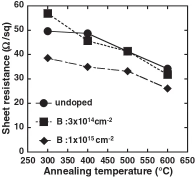
As mentioned above, the epitaxially grown Pd2Si with a
Ti intermediate layer leads to the high thermal stability of Pd silicide layers in Pd/Ti/Si systems with and without B-doping. Figure 7 shows the sheet resistances of Pd/Ti/Si samples as a function of annealing temperature. Sheet resistance decreases with increasing annealing temperature.
This is due to the growth of Pd2Si layers with increasing
RTA temperature, as observed in the XRD measurements shown in Fig. 3. The morphological characteristics of the
Pd2Si surface in Pd/Ti/Si samples with and without
B-doping after annealing at 600C are almost similar; thus, the
sheet resistances should be similar. However, in this study,
the sheet resistance of the Pd2Si layer in the
Pd/Ti/Si-undoped sample is similar to that in the Pd/Ti/Si-B-doped
sample at31014cm2
, while that of the B-doped sample
at 11015cm2
is lower than others. We measured the sheet resistance of the substrate prior to loading it into the vacuum chamber. The sheet resistances of the Si substrate
for the undoped and B-doped samples at31014cm2, and
the B-doped sample at11015cm2 were about 1000 and
100/sq, respectively. Therefore, we consider that the sheet
resistance of the B-doped sample at11015
cm2
decreases owing to the parallel conduction of shallow junctions below the silicide layer.
4. Conclusions
We investigated the growth and thermal stability of Pd silicide thin films on heavily B-doped Si(001) using a Ti
intermediate layer. Epitaxial or highly oriented Pd2Si in
Pd/Ti/Si systems with and without B-doping formed at
annealing temperatures of 300 – 600C. The two orientation
Si002
220
030 & 002
Pd
2Si
Fig. 6. (Color online) TED of Pd/Ti/Si-undoped sample after RTA at 600C for 30 s.
250 300 350 400 450 500 550 600 650 Annealing temperature (°C)
Sheet resistance (
relationships of Pd2Si layers with a Si(001) substrate
were Pd2Si½1 110 kSi½1101 and Pd2Si½110 kSi½001, and
Pd2Si½100 kSi½1110 and Pd2Si½001 kSi½001. The
ag-glomeration of Pd2Si in Pd/Ti/Si could be suppressed by
the epitaxial growth of Pd2Si at 600C with and without
heavy B-doping. It seems that the doping of boron atoms on a Si substrate in a Pd/Ti/Si system does not significantly
affect epitaxial Pd2Si formation.
Acknowledgement
This work was partly supported by the Ministry of Education, Culture, Sports, Science and Technology through a Grant-in-Aid for Scientific Research (A), No. 21246009, 2009.
1) S. Kritzinger and K. N. Tu:J. Appl. Phys.52(1981) 305.
2) H. Tanaka, T. Isogai, T. Goto, A. Teramoto, S. Sugawa, and T. Ohmi: Ext. Abstr. Int. Conf. Solid State Devices and Materials, 2009, p. 332.
3) R. Suryana, S. Akimoto, O. Nakatsuka, and S. Zaima: Ext. Abstr. Advanced Metallization 2008 Conf. 18th Asian Session, 2008, p. 88.
4) L. J. Chen, C. M. Doland, I. W. Wu, J. J. Chu, and S. W. Lu:J. Appl. Phys.62(1987) 2789.
5) S. W. Lu, C. W. Nieh, and L. J. Chen:Appl. Phys. Lett.49(1986) 1770.
6) O. Nakatsuka, K. Okuba, Y. Tsuchiya, A. Sakai, S. Zaima, and Y. Yasuda:Jpn. J. Appl. Phys.44(2005) 2945.
7) O. Nakatsuka, A. Suzuki, S. Akimoto, A. Sakai, M. Ogawa, and S. Zaima:
Jpn. J. Appl. Phys.47(2008) 2402.
8) G. A. Hutchins and A. Shepela:Thin Solid Films18(1973) 343.
9) J. F. Chen and L. J. Chen:Thin Solid Films261(1995) 107.
10) D. M. Hoffman, J. T. McGinn, F. J. Tams, III, and J. H. Thomas, III:
J. Vac. Sci. Technol. A5(1987) 1941.
11) J. T. McGinn, D. M. Hoffman, J. H. Thomas, III, and F. J. Tams: Microsc. Semicond. Mater.87(1987) 535.
12) S. Zaima, J. Kojima, M. Hayashi, H. Ikeda, H. Iwano, and Y. Yasuda:Jpn. J. Appl. Phys.34(1995) 741.
13) M. A. Nicolet and S. S. Lau: inVLSI Electronics Microstructure Science, ed. N. G. Einspruch and G. B. Larrabee (Academic Press, New York, 1983) Vol. 6, Chap. 6, p. 3329.