THESIS – TE 142599
IMPLEMENTATION OF HEVC CODEC ON
FPGA-BASED PLATFORM
OKTAVIA AYU PERMATA 2213 203 019
SUPERVISOR
Dr. Ir. Wirawan, DEA
MASTER PROGRAM
MULTIMEDIA TELECOMMUNICATION FIELD DEPARTMENT OF ELECTRICAL ENGINEERING FACULTY OF INDUSTRIAL TECHNOLOGY INSTITUT TEKNOLOGI SEPULUH NOPEMBER SURABAYA
IMPLEMENTASI HEVC CODEC PADA PLATFORM BERBASIS FPGA
Oleh
:
Oktavia Ayu Permata
NRP
:
2213203019
Pembimbing
:
Dr. Ir. Wirawan, DEA.
ABSTRAK
High Efficiency Video Coding (HEVC) telah di desain sebagai standar baru untuk beberapa aplikasi video dan memiliki peningkatan performa dibanding dengan standar sebelumnya. Meskipun HEVC mencapai efisiensi coding yang tinggi, namun HEVC memiliki kekurangan pada beban pemrosesan tinggi dan loading yang berat ketika melakukan proses encoding video. Untuk meningkatkan performa encoder, kami bertujuan untuk mengimplementasikan HEVC codec pada Zynq 7000 AP SoC.
Kami mencoba mengimplementasikan HEVC menggunakan tiga desain sistem. Pertama, HEVC codec di implementasikan pada Zynq PS. Kedua, encoder HEVC di implementasikan dengan hardware/software co-design. Ketiga, mengimplementasikan sebagian dari encoder HEVC pada Zynq PL. Pada implementasi kami menggunakan Xilinx Vivado HLS untuk mengembangkan codec.
Hasil menunjukkan bahwa HEVC codec dapat di implementasikan pada Zynq PS. Codec dapat mengurangi ukuran video dibanding ukuran asli video pada format H.264. Kualitas video hampir sama dengan format H.264. Sayangnya, kami tidak dapat menyelesaikan desain dengan hardware/software co-design karena kompleksitas coding untuk validasi kode C pada Vivado HLS. Hasil lain, sebagian dari encoder HEVC dapat di implementasikan pada Zynq PL, yaitu HEVC 2D IDCT. Dari implementasi kami dapat mengoptimalkan fungsi loop pada HEVC 2D dan 1D IDCT menggunakan pipelining. Perbandingan hasil antara pipelining inner-loop dan outer-loop menunjukkan bahwa pipelining di outer-loop dapat meningkatkan performa dilihat dari nilai latency.
v
IMPLEMENTATION OF HEVC CODEC ON FPGA-BASED PLATFORM
By
:
Oktavia Ayu Permata
Student Identity Number
:
2213203019
Supervisor
:
Dr. Ir. Wirawan, DEA.
ABSTRACT
High Efficiency Video Coding (HEVC) has been designated as future standard for many video coding application and has significant performance improvement compared to its predecessors. Although HEVC achieves highly efficient coding, it has an impact in higher processing load and severe loading while processing the video encoding. To improve the encoder performance, we aim to implement HEVC codec to Zynq 7000 AP SoC. We try to implement HEVC using three system designs. First, implementation of HEVC codec to Zynq PS as a standalone application. Second, implementation of HEVC encoder as hardware/software co-design. And third, implementing a part of HEVC encoder to Zynq PL independently. In the implementation we use Xilinx Vivado HLS tool to develop the codec.
The results shows that HEVC codec can be implemented on Zynq PS. The codec can reduce the size of video file compared to its original size in H.264 format. The quality of video almost the same compared to H.264 format. Unfortunately we can not finished the work with hardware/software co-design because the coding complexity for validation C code in Vivado HLS. The other result we can get from this project is a part of HEVC codec can be implemented on Zynq PL, which is HEVC 2D IDCT. From the implementation we can optimize the loop function in HEVC 2D and 1D IDCT using pipelining. The compared results between pipelining in inner-loop and in outer-loop shows that pipelining in outer-loop can increase the performance as indicated by increased latency.
vii
ACKNOWLEDGEMENT
This Master’s Thesis would not be possible without the support of scholarship from Ministry of Education and Culture, Republic of Indonesia, the Bureau of Planning and International Cooperation, and the guidence from Pascasarjana’s program of ITS.
I would like to thank to Dr. Wirawan, my supervisor at ITS, for all the meeting and for his valuable comments and advices during the thesis work. His attention and inspiration during the time I spent working with him is invaluable. I would also like to thank him for encouraging my ideas and for giving access to all the facilities in Multimedia Communication Laboratory. All I have learnt through the master’s program and the thesis is something that I will never forget.
I would like to thank to UBO for having trust on me and giving me the possibility of doing half of my thesis with them. I want to thank them for making my stay over the last six months comfortable.
I would like to thank to Xilinx’s forum for all the support, clarifications and guidance that they have given to me during the thesis work. I would like to express my gratitude to all the person involved in my education in both universities, ITS and UBO, that have helped me to improve my skills and my knowledge during the last 2 years. I am really thankful with them due to giving me the opportunity of living this great experience.
Finally, I would like to say that all these would not be possible without the love and support of my families and friends.
ix
1.2 Thesis Scope and Objectives ... 2
1.3 Related Work ... 3
1.4 Thesis Organization ... 3
2 HIGH EFFICIENCY VIDEO CODING 2.1 Overview of HEVC ... 5
2.2 Video Compression Basics ... 6
2.3 Development of HEVC ... 9
2.4 Application Impact ... 10
2.5 How HEVC is Different ... 11
2.6 HEVC and Parallel Processing ... 13
3 ZYNQ 3.1 Overview of System-on-Chip with Zynq ... 15
3.2 Zynq Device ... 16
x
3.2.2 Programmable Logic ... 18
3.2.3 Processing System – Programmable Logic Interfaces ... 20
3.2.4 Comparison: Zynq vs Standard Processor ... 20
3.3 Zynq System-on-Chip Development ... 21
3.3.1 Hardware/Software Partitioning ... 21
3.3.2 Profiling ... 22
3.3.3 Software Development Tools ... 23
3.4 IP Block Design ... 24
3.4.1 IP Core Design Methods ... 24
3.5 High-Level Synthesis ... 24
3.5.1 Vivado HLS ... 26
4 IMPLEMENTATION 4.1 Design Tools ... 29
4.2 System Setup and Requirements ... 29
4.3 Reference Software ... 31
4.3.1 HEVC Test Model (HM) ... 31
4.3.2 Kvazaar ... 32
4.4 System Designs ... 32
4.4.1 HM on Zynq SoC Processing System ... 32
4.4.2 Kvazaar on Hardware/Software co-design ... 41
xi
6 CONCLUSION ... 55
6.1 Conclusions ... 55
6.2 Future Work ... 56
Bibliography ... 59
Appendix A ... 63
xiii
LIST OF FIGURES
Figure 2.1 Scope of video compression standardization... 6
Figure 2.2 Block-based motion compensation ... 8
Figure 2.3 A typical sequence with I-, B-, and P-frames ... 9
Figure 2.4 Expected compression bit rates at time of standardization ... 10
Figure 2.5 H.264 vs HEVC intra prediction modes ... 11
Figure 2.6 An example of a 16x16 H.264 vs MxM HEVC partitions ... 12
Figure 2.7 H.264 macroblock partitions for inter prediction ... 13
Figure 2.8 HEVC quadtree coding structure for inter prediction ... 13
Figure 3.1 Zynq processing system... 17
Figure 3.2 The logic fabric and its constituent elements ... 19
Figure 3.3 The design flow for Zynq SoC ... 22
Figure 3.4 Vivado HLS flow... 25
Figure 3.5 Vivado HLS design flow ... 27
Figure 3.6 Vivado HLS GUI prespectives ... 28
Figure 4.1 Zynq development setup ... 30
Figure 4.2 SDK software development flow ... 33
Figure 4.3 Zynq7 processing system with connection ... 36
Figure 4.4 ZC702 board power switch ... 38
Figure 4.5 Import existing code to SDK ... 40
Figure 4.6 Kvazaar HEVC intra encoder modeled as a state machine ... 41
Figure 4.7 The design step of Vivado HLS ... 43
Figure 4.8 Reviewing the testbench code ... 44
Figure 5.1 Display Sintel video in H.264 vs H.265 format ... 51
xv
LIST OF TABLES
Table 4.1 Parameter to create a new project ... 34
Table 4.2 Parameter to create block design wizard ... 35
Table 4.3 Parameter to create a new application in SDK ... 39
Table 4.4 Kvazaar HEVC encoding parameters used in this design ... 42
Table 5.1 HEVC test in Linux ... 49
Table 5.2 PSNR Kimono in Linux ... 49
Table 5.3 HEVC test on Zynq PS... 50
Table 5.4 PSNR Kimono on Zynq PS ... 50
Table 5.5 Kvazaar profiling... 51
1
Chapter 1
INTRODUCTION
1.1 Background
High Efficiency Video Coding (HEVC) is the recent standard for video compression and has significant performance improvement compared to its predecessor. This new standard is going to be used in many video coding application to fulfill the higher demand on video, especially in resolution which continually increasing. Before HEVC can be widely used, it is necessary to test its performance on appropriate platform based on which typical application will be developed. For this thesis, we aim to implement HEVC codec to Zynq 7000 All Programmable System on Chip, an FPGA-based development system, to test its performance for various scenarios of video application.
Zynq consist of two main architecture: Processing System which has dual-core ARM Cortex-A9 processor and Programmable Logic (PL) which has Field Programmable Gate Array (FPGA) logic fabric. The PS and PL are combined in a single chip. The processor and logic can be used independently or in conjuction. This platform is well-suited for video processing applications, i.e. video compression, because the capability of processing a large amounts of pixel data and software algorithms which can extract information from images (suited to PS and PL, respectively) [1].
Usually when developer want to make an application which can be run on FPGA, they create VHDL or Verilog code that can generate Register Transfer Logic (RTL) for hardware implementation. In traditional FPGA design, creating the system design can take very long time as referred in [1]. Zynq provide a development tools, Vivado High Level System (HLS), that can convert C language directly into RTL code. In this project, Vivado HLS with C-based language is used because it has potential to significantly reduce the design time.
2
using hardware/software co-design. And third, HEVC is implemented in Zynq Programmable Logic (PL) independently. The experiments start from the open-source reference software for HEVC video compression. This software can then be run on the internal processor of the specialized Xilinx Zynq-7000 System on a Chip. This SoC then gives the possibility to execute certain parts in hardware and doing this efficiently will be the main challenge in this thesis.
1.2 Thesis scope and objectives
This thesis has been developed in Multimedia Communication Laboratory of Electrical Engineering Department of ITS. Half of this thesis has been presented to the jury of internship defense from UBO, France. All the hardware and support I have needed has been provided by my supervisor during this time, and we have also received very useful help from Xilinx’s forum during the thesis to understand the tool better. Two versions of open-source reference software for HEVC video compression have been used during the thesis, starting with HEVC test Model (HM) reference software, but during the development of the thesis we changed to an open-source Kvazaar encoder for HEVC intra coding to solve some issues in coding complexity while using hardware/software co-design.
The main objective of this Master’s thesis is to evaluate, Zynq 7000 AP SoC, for the design of HEVC.
These are the objectives of the work:
Get started and familiar with a commercial Vivado tools
Verify the quality of the software-based HEVC, in terms of processing time and size of video
Profiling the open-source reference software for HEVC video compression to know which part need to optimize
Study the coding complexity using Vivado HLS for easier and faster design
3
We have accomplished all these objectives by testing different coding style and tools. For the first step of implementation, we use only the Zynq PS to work with HM. Then we compare the result with linux-based system. The first step has been to evaluate encoder and decoder to learn the different configuration parameters and the limitations of the tool; in other words, to get familiar with the tool. Once this was done, a larger design (hardware/software co-design), will be tested on Zynq 7000 AP SoC. This report describes the latest video compression standard (HEVC), the main uses of Zynq 7000 AP SoC, and how the implementation has been done through the tool.
1.3 Related Work
There are some existing HEVC implementation on FPGA. Some of them is done using HLS implementation such as in [38]. The HLS is used for core functions like intra-prediction that supports all block sizes from 4x4 to 32x32 and achieves 17 frames per second on Alteria Aria II. In [39] it has shown that FPGA implementation can be used for real-time HEVC encoding of 8k video, but it has 17 boards and each capable of encoding full-HD at 60 fps.
Another work is HEVC decoder implementation on FPGA using HLS in [40]. In addition, Verisilicon has created a WebM (VP9) video decoder for Google. They report less than 6 month of the development time, compared to a one year estimate for a traditional RTL approach [41]. The project includes 69k lines of C++ source code, which is much smaller compared to 300k lines of RTL source code.
1.4 Thesis organization
The thesis is organized as follows:
Chapter 2 describes the technical and market implications of HEVC’s adoption in the content creation and delivery market.
4
spans hardware design tools as well as the higher level software tools and flow which include Vivado High Level Synthesis (HLS).
Chapter 4 explain the implementation of HEVC codec on Zynq starting with the design tools, system setup and requirements, reference software, and system designs. Also, the problems and its solutions have been written in each step of implementations.
5
Chapter 2
HIGH EFFICIENCY VIDEO CODING
This chapter contains a brief description of the latest video compression standard, High Efficiency Video Coding (HEVC), which has been used during the thesis. The description focuses on the technical and market implications of HEVC’s adoption in the content creation and delivery market. We will start with the overview of HEVC, an explanation about video compression basics, the development of HEVC, the application impact, and how HEVC is different with the previous standard.
2.1 Overview of HEVC
High Efficiency Video Coding (HEVC), also known as H.265, is an open standard defined by standardization organisations in the telecommunications (ITU-T VCEG) and technology industries (ISO/IEC MPEG) [2]. In every decade, video compression standard has performance improvement compared to the previous standard. For HEVC, it can reduce the overall cost of delivering and storing video while maintaining or increasing the quality of video. HEVC can reduce the size of a video file or bit stream by as much as 50% compared to AVC/H.264 or as much as 75% compared to MPEG-2 standards without sacrificing video quality [3]. This achievements can reduced video storage, transmission costs, and also give the possibility for higher definition content to be delivered for consumer consumption.
6
performance, the development platform can be used to make the compression algorithm parallel and execute everything on hardware.
2.2 Video Compression Basics
The goal of video compression is to remove a redundant information from a video stream so that the video can be sent over a network as efficiently as possible. The process of encoding is used to eliminate the excess of information using an algorithm. Encoding latency is the amount of the time to accomplished encoding process. The decoding process is used to play back the compressed video and return it as closely as possible to its original state. Compression and decompression process, together can form basic codec. The codec is used to reduce the amount of information in a video bit stream.
The general block diagram of a video coding system is shown in Figure 2.1. The general step of video processing can be explained with Figure 2.1 as follow. The raw uncompressed video source is processed in pre-processing block using some of operations such as trimming, color format compression, color correction, or denoising. Then, the encoding block transform the input video sequence into a coded bitstream and package the bitstream into an appropriate format before being transmitted over the channel. In the decoding block, the received bitstream is reconstructed into video sequence. The post-processing block can used the reconstructed video sequence for adaptation of the sequence for display. Finally, the video sequence is ready for viewing in viewing device.
Within a given codec standard, the decoder algorithms are firmly defined, the scope of the standard is generally based around the decoder [4].
7
Encoders within a given standard can vary from vendor to vendor, or even from product to product from a single vendor. This variation is caused by how the designer want to develop certain part of standard using certain tool. Several categories which can be considered during designing including device capabilities, commercial factors, design and development, physical device characteristics, and flexibility.
Encoders do follow these phases and illustrated [5]:
a. Devide each frame into blocks of pixels so that processing can occur simultaneously at a block level.
b. Identify and leverage spatial redundancies that exist within a frame by encoding some of the original blocks via spatial prediction and other coding techniques.
c. Exploit temporal linkages that exist between blocks in subsequent frames so that only the changes between frames are encoded. This is accomplished via motion estimation vectors that predict qualities of the target block.
d. Identify and take advantage of any remaining spatial redundancies that exist within a frame by encoding only the differences between original and predicted blocks through quantization, transform, and entropy coding. During the encoding process, different types of video frames, such as I-frames, P-I-frames, and B-I-frames, may be used by an encoder. When these different frame types are used in combination, video bit rates can be reduced by looking for temporal (time-based) and spatial redundancy between frames that create extraneous information [2]. In this way, objects, or more precisely, pixels or blocks of pixels, that do not change from frame to frame or are exact replicas of pixels or blocks of pixels around them, can be processed in an intelligent manner [5].
8
via motion vector. The motion vector takes fewer bits to encode than an entire block and thereby saves bandwidth on the encoded stream.
Figure 2.2: Block-based motion compensation [2]
An I-frame or intra frame, is a self-contained frame that can be independently decoded without reference to preceding or upcoming images. The first image in a video sequence is always an I-frame and these frame act as starting points if the transmitted bit stream is damaged. I-frames can be used to implement fast-forward, rewind and scene change detection [6]. The lack of I-frames is that they consume many more bits and do not offer compression savings. On the other hand, I-frames do not generate many artifacts because they respresent a complete picture.
A P-frame, which stands for predictive inter frame, references earlier I- or P-frames to encode an image. P-frames typically require fewer bits than I-frames, but are susceptible to transmission errors because of their significant dependency on earlier reference frames [5].
9
Figure 2.3: A typical sequence with I-, B-, and P-frames [2]
These are the basic techniques and objectives of video compression. There are other algorithm involved that transform information about video into fewer and fewer transmitted bits. For futher information can be referred in [7].
2.3 Development of HEVC
HEVC is developed based on previous standard H.264 and both are the output of a joint effort between the ITU-T’s Video Coding Experts Group and the ISO/IEC Moving Picture Experts Groups (MPEG). The ITU-T facilitates creation and adoption of telecommunications standards and the ISO/IEC manages standards for the electronics industries. HEVC is designed to evolve the video compression and intends to [6]:
Deliver an average bit rate reduction of 50% for a fixed video quality compared to H.264
Deliver higher quality at same bit rate
Define a standard syntax to simplify implementation and maximize interoperability
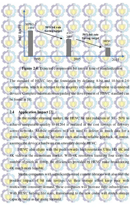
10
Figure 2.4: Expected compression bit rates at time of standardization
The standard of HEVC lays the foundation by defining 8-bit and 10-bit 4:2:0 compression, which is relevant to the majority of video distribution to connected devices. Complete informations regarding the development of HEVC standard can be found in [8].
2.4 Application Impact [2]
In the mobile straming market, the HEVC bit rate reduction of 30 – 50% to achieve comparable quality to H.264 is realized in the cost savings of delivery across networks. Mobile operators will not need to deliver as much data for a given quality level, making for lower costs and more reliable playback, of course, assumes the device’s hardware can smoothly decode HEVC.
HEVC also aligns with the push towards high-resolution Ultra HD 4K and 8K video in the mainstream market. With 4K resolution featuring four times the number of pixels as 1080p, the efficiencies provided by HEVC make broadcasting 4K much more feasible.
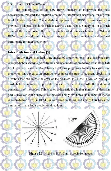
11 2.5 How HEVC is Different
The primary goal of the new HEVC standard is to provide the tools necessary to transmit the smallest amount of information necessary for a given level of video quality. The underlying approach to HEVC is very similar to previously adopted standards such as MPEG-2 and H.264. Simply put: it is much more of the same. While there are a number of differences between H.264 and HEVC, two stand out: increased modes for intra prediction and refined partitioning for inter prediction.
Intra Prediction and Coding [5]
In the H.264 standard, nine modes of prediction exist in a 4x4 block for intra prediction within a given frame and nine modes of prediction exist at the 8x8 level. It’s even fewer at 16x16 block level, dropping down to only four modes of prediction. Intra prediction attempts to estimate the state of adjacent blocks in a direction that minimizes the error of the estimate. In HEVC, a similar technique exist, but the number of possible modes is 35 – in line with the additional complexity of the codec. This creates a dramatically higher number of decision points involved in the analysis, as there are nearly two times the number of spatial intra-prediction sizes in HEVC as compared to H.264 and nearly four times the number of spatial intra-prediction directions.
12 Inter Prediction and Coding [5]
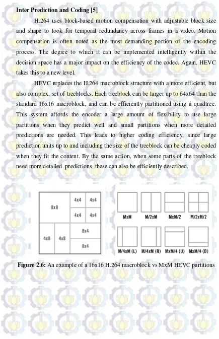
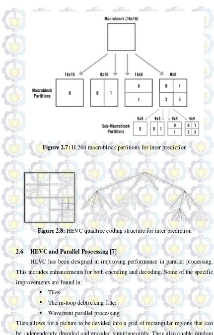
H.264 uses block-based motion compensation with adjustable block size and shape to look for temporal redundancy across frames in a video. Motion compensation is often noted as the most demanding portion of the encoding process. The degree to which it can be implemented intelligently within the decision space has a major impact on the efficiency of the codec. Again, HEVC takes this to a new level.
HEVC replaces the H.264 macroblock structure with a more efficient, but also complex, set of treeblocks. Each treeblock can be larger up to 64x64 than the standard 16x16 macroblock, and can be efficiently partitioned using a quadtree. This system affords the encoder a large amount of flexibility to use large partitions when they predict well and small partitions when more detailed predictions are needed. This leads to higher coding efficiency, since large prediction units up to and including the size of the treeblock can be cheaply coded when they fit the content. By the same action, when some parts of the treeblock need more detailed predictions, these can also be efficiently described.
13
Figure 2.7: H.264 macroblock partitions for inter prediction
Figure 2.8: HEVC quadtree coding structure for inter prediction
2.6 HEVC and Parallel Processing [7]
HEVC has been designed in improving performance in parallel processing. This includes enhancements for both encoding and decoding. Some of the specific improvements are found in:
Tiles
The in-loop deblocking filter
Wavefront parallel processing
14
access to specific regions of a picture in a video stream.
In the case of the in-loop deblocking filter, it has been defined such that it only applies to edges aligned on an 8x8 grid in order to reduce the number of interactions between blocks and simplify parallel processing methodologies. The processing order has been specified as horizontal filtering on vertical edges followed by vertical filtering of horizontal edges. This allows for multiple parallel threads of deblocking filter calculations to be run simultaneously.
15
Chapter 3
ZYNQ
This chapter cover the essential information about the platform we used in the project; Zynq. Before getting started with the project, we have to know how Zynq work and how to use it. The contents of this chapter includes an overview of System-on-Chip with Zynq, the main architecture of Zynq, the development of Zynq, IP block design, and also a description of high level synthesis (HLS) and its tool like Vivado HLS.
3.1 Overview of System-on-Chip with Zynq [1]
Xilinx gave their new device the name Zynq, because it represents a processing element that can be applied to anything. Zynq devices are intended to be flexible and form a compelling platform for a wide variety of applications, just as the metal zync can be mixed with various other metals to form alloys with different desirable properties.
16 3.2 Zynq Device
The general architecture of the Zynq comprises two sections: the Processing System (PS), and the Programmable Logic (PL). These can be used independently or together. However, the most compelling use model for Zynq is when both of its constituent parts are used in conjunction. The architecture of Zynq is reviewed over this section, starting with the PS and PL. Extended information can be found in the
Zynq-7000 Technical Reference Manual [10].
3.2.1 Processing System
All Zynq devices have the same basic architecture, and all of them contain, as the basis of the processing system, a dual-core ARM Cortex-A9 processor. Importantly, the Zynq processing system encompasses not just the ARM processor, but a set of associated processing resources forming an Application Processing Unit (APU), and further peripheral interfaces, cache memory, memory interfaces, interconnect, and clock generation circuitry [9]. A block diagram showing the architecture of the PS is shown in Figure 3.1, where the APU is highlighted.
Application Processing Unit (APU) [1]
17
8-bit Java bytecodes (used for Java Virtual Machines) when in the appropriate state. For further information about instruction set options and details can be found in [11].
Figure 3.1: Zynq processing system [1]
The ARM Model
18 Processing System External Interfaces
Communication between the PS and external interfaces is achieved primarily via the Multiplexed Input/Output (MIO). Certain connections can also be made via the Extended MIO (EMIO), which is not a direct path from the PS to external connections, but instead passes through and shares the I/O resources of the PL.
The available I/O includes standard communications interfaces, and General Purpose Input/Output (GPIO) which can be used for a variety of purposes including simple buttons, switches, and LEDs. Extensive further information about each of these interfaces is available in the Zynq-7000 Technical Reference Manual [10].
3.2.2 Programmable Logic [1]
The second principal part of the Zynq architecture is the programmable logic. This is based on the Artix-7 and Kintex-7 FPGA fabric. The PL part of the Zynq device is shown in Figure 3.2, with various features highlighted. The PL is predominantly composed of general purpose FPGA logic fabric, which is composed of slices and Configurable Logic Blocks (CLBs), and there are also Input/Output Blocks (IOBs) for interfacing.
Features of the PL (shown in Figure 3.2) can be summarised as follows:
Configurable Logic Block (CLB) ; CLBs are small, regular groupings of logic elements that are laid out in a two-dimensional array on the PL, and connected to other similar resources via programmable interconnects. Each CLB is positioned next to a switch matrix and contains two logic slices.
Slice ;A sub-unit within the CLB, which contains resources for implementing combinatorial and sequential logic circuits. Zynq slices are composed of 4
Lookup Tables, 8 Flip-Flops, and other logic.
19
together to form larger logic functions, memories, or shift registers, as required.
Figure 3.2: The logic fabric and its constituent elements [1]
Flip-flop (FF) ; A sequential circuit element implementing a 1-bit register, with reset functionality. One of the FFs can optionally be used to implement a latch.
20
Carry logic; Arithmetic circuits require intermediate signals to be propagated between adjacent slices, and this is achieved via carry logic. The carry logic comprises a chain of routes and multiplexers to link slices in a vertical column.
Input / Output Blocks (IOBs); IOBs are resources that provide interfacing between the PL logic resources, and the physical device ‘pads’ used to connect to external circuitry. Each IOB can handle a 1-bit input or output signal. IOBs are usually located around the perimeter of the device.
Although it is useful for the designer to have a knowledge of the underlying structure of the logic fabric, in most cases there is no need to specifically target these resources. The Xilinx tools will automatically infer the required LUTs, FFs, IOBs etc. from the design, and map them accordingly.
3.2.3 Processing System – Programmable Logic Interfaces
As mentioned in the previous section, the appeal of Zynq lies not just in the properties of its constituent parts, the PS and the PL, but in the ability to use them in tandem to form complete, integrated systems. The key enabler in this regard is the set of highly specified AXI interconnects and interfaces forming the bridge between the two parts. There are also some other types of connections between the PS and PL, in particular EMIO. Extended information can be found in [10].
3.2.4 Comparison: Zynq vs Standard Processor
21 3.3 Zynq System-on-Chip Development
In this section we will describe the Zynq design flow that concentrate on software development in general. This section explore the important concept of hardware/software partitioning, Zynq software development, and profiling.
3.3.1 Hardware/Software Partitioning [1]
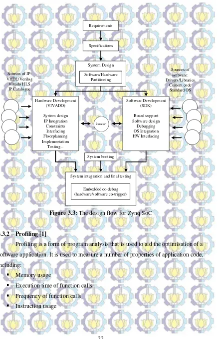
Hardware/software partitioning, also known as hardware/software co-design, is an important stage in the design of embedded systems and, if well executed, can result in a significant improvement in system performance. The process of hardware/software partitioning involves deciding which system components should be implemented in hardware and which should be implemented in software. The reason behind the partitioning process is that hardware components, FPGA programmable logic fabric, are typically much faster due to the parallel processing nature of FPGA devices. Software components, on the other hand, implemented on a GPP or a microprocessor, are both to create and maintain, but are also slower due to the inherent sequential processing. The design flow for hardware/software partitioning in Zynq SoC is shown in Figure 3.3.
22
System integration and final testing
Embedded co-debug
Figure 3.3: The design flow for Zynq SoC
3.3.2 Profiling [1]
Profiling is a form of program analysis that is used to aid the optimisation of a software application. It is used to measure a number of properties of application code, including:
Memory usage
Execution time of function calls
Frequency of function calls
23
Profiling can be performed statically (without executing the software program) or dynamically (performed while the software application is running on a physical or virtual processor). Static profiling generally performed by analysing the source code, or sometimes the object code, whereas dynamic profiling is an intrusive process whereby the execution of a program on a processor is interrupted to gather information.
The use of profiling allows us to identify bottlenecks in the code execution that may be a result of inefficient code, or poor communication between function interactions with a module in the PL or another function within software. It could also be the case that the algorithm may more suitable for implementation in hardware. Once identified, the bottlenecks can be optimised by rewriting the original software function or by moving it to the PL for acceleration.
3.3.3 Software Development Tools
Software application development flows for the Zynq-7000 AP SoC devices allow the user to create software applications using a set of Xilinx tools, as well as utilising a wide range of tools from third-party vendors which target the ARM Cortex-A9 processors [14].
Xilinx provides design tools for the development and debugging of software applications for Zynq-7000 AP SoC devices. Provided software includes: software IDE, GNU-based compiler toolchain, JTAG debugger, and various other associated utilities.
Xilinx provides two hardware configurations tool which provide support for the Zynq-7000 AP SoC devices. These are: Vivado IDE design suite IP integrator and ISE design suite embedded development kit (EDK) Xilinx platform studio (XPS).
24
debugger, utilities, and libraries), JTAG debugger, flash programmer, driver for Xilinx’s IP, etc. All of the features that have been mentioned are accessible from within the Eclipse-based IDE, which incorporates the C/C++ Development Kit (CDK). For further and complete information can be referred in [14].
3.4 IP Block Design
IP block or IP core is a hardware specification that can be used to configure the logic resources of an FPGA or for other silicon devices, physically manufacture an integrated circuit [15]. In term of IP cores, there are two types: hard IP cores and soft IP cores. Further information can be found in [1].
3.4.1 IP Core Design Methods
Xilinx provide a number of tools which enable the creation of custom IP blocks for use in our own embedded system designs. There are HDL, System generator, HDL coder, and Vivado High Level Synthesis. For this project, we use Vivado High Level Synthesis for designing the IP core. Figure 3.4 show an overview of Vivado HLS design flow. Vivado HLS is a tool provided by Xilinx, as a part of the Vivado Design Suite, which is capable of converting C-based design (C, C++ or SystemC) into RTL design files (VHDL/Verilog or System C) for implementation of Xilinx All Programmable devices. Vivado HLS will be described in detail in the next section.
3.5 High-Level Synthesis
Before proceeding to the description of Vivado HLS tool, it is important to establish some information about high level synthesis.
25
relevant and has emerged as a possible substitution of the RTL description, to shorten the development time of new hardware devices.
Figure 3.4: Vivado HLS flow [1]
26
The languages uses for HLS are predominantly C-based, including C, C++, and SystemC as supported in Vivado HLS.
3.5.1 Vivado HLS
Vivado HLS transforms a C, C++ or SystemC design into an RTL implemen-tation, which can then be synthesised and implemented onto the programmable logic of a Xilinx FPGA or Zynq device [17].
In performing HLS, the two primary aspects of the design are analysed:
The interface of the design, i.e. its top-level connections, and
The functionality of the design, i.e. the algorithm that it implements.
27
Figure 3.5: Vivado HLS design flow [1]
28
Figure 3.6: Vivado HLS GUI perspectives
29
Chapter 4
IMPLEMENTATION
In this chapter we are going to explain the implementation of HEVC codec on Zynq development platform. The explanations start with the implementation of HEVC codec to Zynq PS, then the implementation as hardware/software co-design, and the implementation to Zynq PL. Those three implementations is our effort to make hardware encoder for HEVC. Although some of implementation can not be finished yet, but in this chapter I try to give all the explanation for all the experiments that I have tried during the work. The problems and the solutions are also written in each designs step.
4.1 Design Tools
To start designing for Zynq, we need to obtain the appropriate design tools from Xilinx. These can be ordered on DVD, or downloaded from Xilinx website. There are a number of design tools available, but we need only these:
Vivado Design Suite (version 2014.1 or later)
License Management Tools (2014.1 Utilities or later)
We need also to install some properties from the Xilinx Tools depending on our requirements.
4.2 System Setup and Requirements
As general statement from Xilinx, recent versions of Windows and selected versions of Linux are supported. For this project, we use Ubuntu 14.04 LTS as operating system. When using Vivado, it is important that the operating system grants the user write permissions for all directories containing design files.
30
CPU Intel core i7 with 4GB RAM (64-bit system). The computer hardware configuration also requires a USB port for programming the Zynq over JTAG, and ideally another for PC-Zynq communication via the UART and Terminal application for debugging designs.
For prototyping and testing the design, we use the Xilinx ZC702 Rev 1.0 evaluation board. A development board hosts a Zynq device, together with various other resources such as power circuitry, external memory, interfaces for programming and communication, simple user I/O such as buttons, LEDs, switches, and usually a number of other peripheral interfaces and connectors. During the debugging stage, designs developed on the computer using the Vivado design suite can be downloaded onto the development board using a Joint Test Action Group (JTAG) or ethernet connection, then tested in hardware using peripherals and external interfaces if required. Debugging may include, for instance: using a debugger to interact with the processor and monitor its behaviour; user interaction with the design running on the chip via a USB-UART connection and the Terminal interface on the PC; and by executing hardware-in-the-loop simulations with the aid of an ethernet connection.
Figure 4.1 provide a graphical summary of a typical setup for getting started with Zynq.
31 4.3 Reference Software
Reference software take an important role as source code for this project. Up to this date, several HEVC encoders have been released but most of them are commercial products whose features and operating principles are kept confidential. Therefore, we use open-source encoders for this project.
Among the existing open-source HEVC encoders, only HEVC test model (HM), x265, f265, and Kvazaar HEVC encoder are under active development. HM as an HEVC reference codec is able to achieve the best coding efficiency among the existing HEVC encoders, but its object-based C++ implementation results in poor performance. Hence, it is targeted for research and conformance testing rather than practical encoding. The commercially funded x265 is the most well-known practical open-source HEVC encoder. It is based on HM C++ source code which has been enhanced by extensive assembly optimizations, multithreading, and techniques from the open-source x264 encoder. f265 is another industrial HEVC encoder. It is implemented in C with assembly optimizations. Although the source codes for these two commercially led projects are under open-source licenses, contributors to these projects must sign an agreement giving the companies copyright to their work. Requiring such agreements leaves room for non-commercial projects, like Kvazaar, that do not require signing separate agreements to participate. Kvazaar is an academic open-source HEVC encoder initiated and coordinated by Ultra Video Group [27]. It is licensed under GNU GPLv2 license [24].
Considering the usage of all open-source HEVC encoders, I initiate to use HM and Kvazaar as reference software for this project.
4.3.1 HEVC Test Model (HM)
32
we use encoder_intra_main.cfg as the configuration. HM is used in implementation to Zynq PS and Zynq PL, independently.
4.3.2 Kvazaar
Kvazaar uses a reverse design approach compared with x265. It has been developed from HM primarily as a reference for its encoding scheme and individual algorithm implementations, but it adopts completely new data and function call tree structures. Kvazaar is developed in C. This more hardware-oriented approach eases source code acceleration, portability, and parallelization [24]. The source codes and issue tracker for Kvazaar can be found on its GitHub page [26]. Kvazaar version 0.72 is used in this experiments.
4.4 System Designs
In this section we are going to explain the system designs we have used in the project. We have three system designs because we try to experiment the close possibility of HEVC which can be implemented and work properly on Zynq ZC702. Each of designs gives the explanation about the trials and errors during the work. The following section will discuss how I implement open-source HEVC to Zynq PS and Zynq PL, independently, and as hardware/software co-design.
4.4.1 HM on Zynq SoC Processing System
We will begin using Xilinx Vivado Design Suite to develop an embedded system (codec) using the Zynq 7000 AP SoC Processing System (PS). As we mentioned before, Zynq SoC consists of ARM Cortex-A9 hard intellectual property (IP) and programmable logic (PL). This offering can be used in two ways:
The Zynq SoC PS can be used in a standalone mode, without attaching any additional fabric IP.
33
In this design, I implement HM to Zynq PS as a standalone application. Vivado Design Suite is used to create a project with an embedded processor system as the top level. Figure 4.2 ilustrate the SDK software development flow for this design.
Hardware platform exported from Vivado to SDK
Create an SDK workspace
Create a BSP
Create a software project
Develop the software application (HM)
Generate a linker script
Download the hardware bitstream to the FPGA device
Profile software application
Debug software application Run software application
Figure 4.2: SDK software development flow
From Figure 4.2 I have knowledge that I won’t be able to import the open-source HM directly into a Xilinx SDK workspace unless I developed the existing project in Xilinx SDK. So first, I create a fresh workspace and create a Xilinx SDK
Makefile project from our existing source code. Then I can edit the resulting
34 Step 1: Create a new project
To create a new project in Vivado design tool, we need to make selections in each of the wizard screen. Table 4.1 show informations to create a new project using this design.
Tabel 4.1: Parameter to create a new project
Wizard Screen System Property Setting or Command to Use Project name Project name edt_tutorial
Project location /opt/Xilinx/Vivado/……/bin Create project
subdirectory
Leave this checked
Project type Specify the type of sources for the design.
RTL Project
Do not specify sources at this time
Leave this unchecked
Add Sources Do not make any changes to this screen Add existing IP Do not make any changes to this screen Add constraints Do not make any changes to this screen
Default part Select Boards
Board Zynq-7 ZC702 Evaluation
Board New project
summary
Project summary Review the project summary before clicking Finish to create the project
Step 2: Create an Embedded Processor Project
35
device IP options, and double-click the ZYNQ7 Processing System IP to add it to the Block Design. Then the Zynq SoC processing system IP block appears in the Diagram view.
Table 4.2: Parameter to create block design wizard
Wizard Screen System Property Setting or Command to Use Create Block Design Design name tutorial_bd
Directory <Local to Project> Specify source set Design Sources
Step 3: Managing the Zynq7 Processing System in Vivado
We have added the processor system to the design, then we can begin by managing the various options available for the Zynq7 Processing System.
When we double-click the ZYNQ7 Processing System block in the Block Diagram window, the Re-customize IP dialog box opens. By default, the processor system does not have any peripherals connected. Connections are symbolized with check marks. We use a preset template created for the ZC702 board. This configuration wizard enables many peripherals in the Processing System with some MIO pins assigned to them as per the board layout of the ZC702 board. For example, UART1 is enabled and UART0 is disabled. This is because UART1 is connected to the USB-UART connector through UART to the USB converter chip on the ZC702 board. The check marks that appear next to each peripheral name in the Zynq device block diagram signify the I/O Peripherals that are active. After Vivado implements the changes that we made to apply to ZC702 board presets, the message stating that Designer assistance is available. We can use Run Block Automation link to accept the default processor system options and make default pin connections.
Step 4: Validating the Design and Connecting Ports
36
connected. From Block Diagram view of the ZYNQ7 Processing System, we can hover our mouse over the connecter port until the pencil icon appears. Click the M_AXI_GP0_ACLK port and drag to the FCLK_CLK0 input port to make a connection between the two ports. Then validate the design again to ensure there are no other errors. Figure 4.3 show the ZYNQ7 Processing System with Connection.
Figure 4.3: ZYNQ7 processing system with connection
In the Block Design view, under the Sources tab, we can create HDL wrapper file for the processor subsystem. We can select Let Vivado manage wrapper and auto-update, then select Generate Output Products. This step builds all required output products for the selected source. For example, constraints do not need to be manually created for the IP processor system. Vivado automatically generates the .XDC file for the processor sub-system when Generate Output Products is selected. We can find the output products that we just generated in IP Source directory.
Step 5: Synthesizing the Design, Running Implementation, and Generating the Bitstream
37 Step 6: Exporting to SDK
We can launch SDK from Vivado with the Export Hardware command. Make sure that the Include bitstream check box is checked only when design has PL design and bitstream generated, and that the Export to field is set to the default option of <Local to Project>. Notice that when SDK launches, the hardware description file is automatically loaded. The system.hdf tab shows the address map for the entire Processing System.
So far, Vivado has exported the hardware specifications to the selected workspace where software development will take place. If <Local to Project> was selected, then Vivado created a new workspace in the Vivado project folder. The name of the workspace is <project_name>.sdk. In this project, the workspace created is /opt/Xilinx/Vivado/…/bin/edt_tutorial/edt_tutorial.sdk.
The Vivado design tool exported the Hardware Platform Specification for the design (system.hdf) to SDK. In addition to system.hdf, the following additional files are exported to SDK:
design_1_bd.tcl
38 Step 7: Running the HM Application
We will learn how to manage the board settings, make cable connections, connect to the board through PC, and run a HM software application in SDK.
We can connect the power cable to the board using digilent cable with the following SW10 switch setting: bit-1 is 0 (switch open), bit-2 is 1 (switch closed). Then connect USB cable to connector J17 on the target board with the Linux host machine for USB to serial transfer. And the ZC702 board is ready to switch on. In the SDK, we can ensure the workspace path to the project file, which is /opt/Xilinx/Vivado/…/bin/edt_tutorial/edt_tutorial.sdk.
Figure 4.4: ZC702 board power switch
Now we can make serial connection. First we have to know which port is used to connect with board. For checking the active port, we can type dmesg in terminal Linux. A lot of active port will be shown. We can see the name of port that used to connect to the board. Then we can make serial connection through SDK. In terminal SDK, we can modify the setting to make the connection.
39
Table 4.3: Parameter to create a new application in SDK
Wizard Screen System Properties Setting or Command to Use Application
Project
Project name HM_encoder
Use default location Select this option
Hardware platform tutorial_bd_wrapper_hw_platform_0 Processor PS7_cortexa9_0
OS platform standalone
Language C++
Board Support Package
Select Create New and provide the name of HM_encoder_bsp
Templates Available templates Empty Application
The board support package (BSP) is the support code for a given hardware platform or board that helps in basic initialization at power up and helps software applications to be run on top of it. It can be specific to some operating systems with bootloader and device drivers [30].
Standalone is a simple, low-level software layer. It provides access to basic processor features such as caches, interrupts, and exceptions, as well as the basic processor features of a hosted environment. These basic features include standard input/output, profiling, abort, and exit. It is a single threaded semi-hosted environment. The application we ran in this section was created on top of the Standalone OS. The BSP, software application targets, is selected during the New Application Project creation process. If we would like to change the target BSP after project creation, we can manage the target BSP by right-clicking the software application and selecting Change Referenced BSP [30].
40
the SDK, we need to create our own makefile. So we can import the makefile from open-source HM to SDK.
Figure 4.5: Import existing code to SDK
41
4.4.2 Kvazaar on Hardware/Software co-design
In this section, I try to implement open source Kvazaar HEVC encoder to Zynq 7000 AP SoC as hardware/software co-design using Vivado HLS. The source code I use for this design is Kvazaar because its less complex than HM and Kvazaar use C language that make it more hardware-friendly. In this experiment, I focus on all-intra coding configuration of Kvazaar. Figure 4.6 show a state machine model of Kvazaar HEVC intra encoder to illustrate its computational complexity. This design is intended to focus on a rapid implementation of the HEVC encoder through a HLS flow.
42
Kvazaar intra encoder supports HEVC all-intra coding of 8-bit video with 4:2:0 chroma sampling. The parameter listed in Table 4.4 is used in this design. We use Kvazaar version 0.72 for this experiment.
Table 4.4: Kvazaar HEVC coding parameters used in this design
Features Kvazaar HEVC intra encoder
Profile Main
Internal bit depth, color format 8, 4:2:0
Coding modes Intra
Sizes of luma coding blocks 64x64, 32x32, 16x16, 8x8 Sizes of luma transform blocks 32x32, 16x16, 8x8, 4x4
Sizes of luma prediction blocks 64x64, 32x32, 16x16, 8x8, 4x4 Intra prediction modes DC, planar, 33 angular
Mode decision metric SAD
RDO Disabled
RDOQ Disabled
Transform Integer DCT (integer DST for luma
4x4) 4x4 transform skip Enabled
Loop filtering DF, SAO
The design step can be shown in Figure 4.7. Before we start create a new project, the first phase, functional verification, is done on PC using ready-made
make for Linux GCC compiler. The next step is profiling for early performance estimation, in which I use Gprof, gprof2dot, and Graphviz. Potential functions for hardware acceleration are selected by examining the Gprof results.
43
Search_intra_rough function calls intra_get_pred function to calculate the prediction for all 35 modes, then calculates the Sum of Absolute Difference (SAD) for all these modes, and finally returns the costs for all modes through a pointer passed to the function (Figure 4.6). These functions are the most potential candidates for hardware acceleration. Based on Gprof profiling results, a new project in Vivado HLS is created for design space exploration and hardware/software partitioning.
Create a new project in Vivado HLS
Figure 4.7: The design step of Vivado HLS
Step 1: Create new project
44
of ZC702 board. The solution holds information on the target technology, design directives, and results.
Step 2: Validate the C source code
The first step in an HLS project is to confirm that the C code is correct. This process is called C Validation or C Simulation. In this design, the test bench compares the output data from the encmain function with known good values.
Figure 4.8: Reviewing the testbench code
The test bench file, contains the top-level C function main(), which in turn calls the function to be synthesized (encmain). Then we can Run C Simulation to compile and execute the C design.
45 Problems :
Can not find header file
For this problem we can solve it by using Edit CFLAGS button to add the standard gcc/g++ search path information. For example, -I<path_to_header_file_dir>
Integer data type
In the encmain.c there are a lot of looping. And each looping in C language declare the data type in its inner loop while Vivado HLS require to declare the data type in its outer loop. So I manage to declare the data type in its outer loop. Again, standard C compilers such as gcc compile the attributes used in the header file to define the bit sizes, but they do know what they means. The final executable created by standard C compiler will issue messages such as the following
$VIVADO_HLS_ROOT/include/etc/autopilot_dt.def:1036: warning: bit-width attribute directive ignored
and proceed to use native C data types for the simulation and producing results which do not reflect the bit-accurate behavior of the code. Those can be solved by enabling apcc compiler in the project setting using menu Project > Project Settings > Simulation and select Use APCC for Compiling C Files. Apcc will overcomes this limitation and allows the function to be compiled and verified in a bit-accurate manner.
Unsupported C language construct
While High-Level Synthesis is able to synthesize a large subset of all three C modeling standards (C, C++ and SystemC) there are some constructs which cannot be synthesized such as pointer casting. Pointer casting is not supported in the general case but is supported between native C types. The following is not synthesizable and must be transformed, and I do not know how to transform these pointer casting type yet.
46
/// \brief Number of bytes filled in this chunk. uint32_t len;
/// \brief Next chunk in the list. struct kvz_data_chunk *next;
} kvz_data_chunk;
4.4.3 HM on Zynq Programmable Logic
Because I can not continue working with hardware/software partitioning, I try to implement HEVC on Zynq Programmable Logic independently. I use HM as the source code because I want to know the performance of HM when implemented on Zynq PL. And also, the system design before this has been implemented HM on Zynq PS. After studying the coding, unfortunately, I can not use the full HM as a source code. There will be another problem like in the design before while try to run C simulation. So I decide to take a part of HM which is IDCT to implement on Zynq PL.
4.4.3.1HEVC Inverse DCT Using Vivado HLS
Since HEVC 2D IDCT performs matrix multiplication operations, it is suitable for HLS implementation. HEVC IDCT algorithm is one of the most computationally complex algorithms compared to other HLS implementation for both image processing and video compression. IDCT inputs are selected depending on size of the IDCT operation (4x4, 8x8, 16x16 or 32x32). First, 1D column IDCT is performed, and the resulting coefficients are clipped. Then, 1D row IDCT is performed using transpose of the resulting matrix as input, and the resulting coefficients are clipped.
47
A part of C codes developed as input to Vivado HLS is shown in Figure 4.9. Because HEVC 2D IDCT perform matrix multiplication operations, many for loops are used in the C codes. Therefore, loop unrolling directive is used in the C codes to increase performance. Pipelining directives is also used in the C codes to increase performance.
void COL_partialButterflyInverse8(
int15 resid[DCT_8], int7 coeff[31], int7 coef8[16], int16 *Y1, int16 *Y2, int16 *Y3, int16 *Y4,
int16 *Y5, int16 *Y6, int16 *Y7, int16 *Y8) {
char j,l,k = 0;
int26 E[4], O[4], EE[2], EO[2]; for(l=0; l<4; l++)
#pragma HLS unroll factor=2
{O[l] = coef8[l*4]*resid[1] + coef8[l*4+1]*resid[3] + coef8[l*4+2]*resid[5] + coef8[l*4+3]*resid[7];
};
EO[0] = coeff[1]*resid[2] + coeff[2]*resid[6]; EO[1] = coeff[2]*resid[2] - coeff[1]*resid[6]; EE[0] = coeff[0]*resid[0] + coeff[0]*resid[4]; EE[1] = coeff[0]*resid[0] - coeff[0]*resid[4];
#pragma HLS pipeline
49
Chapter 5
Results
This chapter shows the result of implementation open-source HEVC on Zynq 7000 AP SoC. Unfortunately, we can not obtain the result from hardware/software co-design because of the coding complexity. Still, we have the results from the implementation of HEVC to Zynq PS and Zynq PL independently.
5.1 Performance in Linux vs Zynq PS
In this section, we compare two results from HM 16 which have been run in Linux and Zynq PS. The implementation results includes the comparison of video size after being compressed, processing time of encoding and decoding video, and the video quality of HEVC codec. We use two video file in YUV format for input of video compression; Kimono.yuv and Sintel.yuv. Both of the video have the same resolution 1920x1080p and same fps 24 which relevance with minimum fps for HD video. We use encoder_intra_main.cfg as configuration parameter with QP = 32.
A. Run in Linux
Table 5.1: HEVC test in Linux Input
Table 5.2: PSNR Kimono in Linux
Y-PSNR U-PSNR V-PSNR YUV-PSNR
38,9512 41,1150 42,0501 39,5547
50
frame the video have, the longer time to encode and decode video. HM 16 is obviously can reduce the video size of video, although the percentage of decreased size of video is not stable. As stated in the HM guide, this reference software is not intended to prove the ability of HEVC standard which can reduce the size of video halve of its predecessor. If we want to reduce the size of video up to 50%, we need to modify the configuration parameter in HM. The results also show that HM 16 can work faster on Zynq PS than in Linux.
B. Run on Zynq PS
Table 5.4: PSNR Kimono on Zynq PS
Y-PSNR U-PSNR V-PSNR YUV-PSNR
38.8394 41.9582 39.5621 38.4775
From Table 5.1 and Table 5.3, the processing time of Zynq PS is 5% faster than Linux. HM 16 can not obtain optimal processing time when used in Zynq PS. This probably because the selection criteria when designing HM 16 is not intended in fast processing speed. Also, the algorithm in HM 16 is quite complex which can results in high processing load of encoding video in processor.
51
Figure 5.1: Display Sintel video in H.264 vs H.265 format
5.2 Profiling
Profiling is used before implementing Kvazaar on hardware/software co-design. Profiling can define which processing block of the Kvazaar HEVC intra coding need to optimize. Table 5.5 show the result of profiling Kimono 1080p in Kvazaar using Gprof.
Table 5.5: Kvazaar profiling
Functions Time consuming for encoding intra prediction 67,74%
quantization 8,54%
dst/dct 4,69%
inverse dst/dct 3,78%
dequantization 0,95%
52
development time and make the design simple, but it requires the knowledge about the development behaviour of HLS first. The problems and solutions in this design have been explained in the previous chapter.
5.3 Zynq PL
In this section, a part of HEVC was implemented using Vivado HLS to Zynq PL. The results from implementing HEVC 2D IDCT using Vivado HLS can be described as follow. In the hardware, IDCT inputs are selected depending on size of the IDCT operation (4x4, 8x8, 16x16 or 32x32). The hardware uses an efficient butterfly structure for column and row transforms. After 1D column IDCT, the resulting coefficients are stored in a transpose memory, and they are used as input for 1D row IDCT. The multiplication operations are performed in the datapaths using only adders and shifters. There are 4 multiplier blocks in 8x8 datapath, 8 multiplier blocks in 16x16 datapath and 16 multiplier blocks in 32x32 datapath.
Another experiment was adding pipelining directives to the loops and review for loop optimization. Pipeline is added to the inner-loop and outer-loop of HEVC 1D IDCT and 2D IDCT. Figure 5.2 show the comparison results of pipelining in inner-loop and pipelining in outer-loop.
53
Figure 5.2 shows the results of comparing solution 1, solution2, and solution3. Solution 1 is the result of original design without pipelining, Solution 2 is the results of pipelining the inner-loop of HEVC 1D and 2D IDCT, Solution 3 is the results of pipelining the outer-loop of HEVC 1D and 2D IDCT. From the the three solution, pipelining the outer-loop has in fact resulted in performance improvement. The significant latency benefit is achieved because multiple loops in the design call the dct_1d function multiple times. Saving latency in this block is multiplied because this function is used inside many loops. Pipelining loops transforms the latency from
Latency = iteration latency * (tripcount * interval)
to
Latency = iteration latency + (tripcount * interval)
After reviewing the loop optimization, the design of Solution 3 is used to run C synthesis. Table 5.6 shows the results of implementation HEVC 2D IDCT using Vivado HLS.
Table 5.6: Xilinx Vivado HLS implementation results TU LUTs DFFs Slices BRAMs I/O
54 5.4 Processor Operation in Zynq PS
The resources of a processor are fixed, and limited to two processing cores, which are required to operate at a specific clock frequency. The cost of implementing a desired software implementation is measured in terms of clock (execution) cycles, which will of course require some specific amount of time to execute at the desired clock frequency; the more complex the required processing, the longer the execution time will be.
55
Chapter 6
Conclusion
At the end of this Master’s Thesis I am glad that I have tried to implement HEVC codec on Zynq 7000 AP SoC with three system designs. First, I try to implement HEVC codec to Zynq PS as standalone application. Second, I try to implement HEVC encoder to Zynq 7000 AP SoC as hardware/software co-design. Although in this design I can not finished the work, I’m glad at least I know the flow to work with hardware/software co-design. And also, we got the result from profiling HEVC encoder. Thrid, I try to implement HEVC encoder to Zynq PL.
6.1 Conclusions
From the three experiments that have been done, I can conclude that:
1. HM 16 can be run on Zynq PS and can reduce the size of video up to 50% of the original video format (YUV). From the quality video, HM 16 appeared to be very close to the one of the original video in H.264 format. This design can be used for delivering high quality video while maintaining the storage.
2. Profiling can be used to analyze HEVC encoder to find the function that consume a lot of time during encoding process. Intra prediction consume 67,74% time in encoding process. Those function can then be optimized in hardware part.
3. HM 16 also can be run on Zynq PL using Vivado HLS. The important part in this design is optimizing the loop using pipelining. Pipelining the outer-loop can increase the latency 2x faster than using original design. In this experiment, I still do not use video file as input. The results is based on the synthesis of C simulation from HEVC 2D IDCT using Vivado HLS.
![Figure 2.1: Scope of video compression standardization [4]](https://thumb-ap.123doks.com/thumbv2/123dok/1801445.2098706/21.595.82.517.90.768/figure-scope-of-video-compression-standardization.webp)
![Figure 2.2: Block-based motion compensation [2]](https://thumb-ap.123doks.com/thumbv2/123dok/1801445.2098706/23.595.81.518.87.768/figure-block-based-motion-compensation.webp)
![Figure 2.3: A typical sequence with I-, B-, and P-frames [2]](https://thumb-ap.123doks.com/thumbv2/123dok/1801445.2098706/24.595.82.514.83.765/figure-typical-sequence-i-b-p-frames.webp)
![Figure 3.1: Zynq processing system [1]](https://thumb-ap.123doks.com/thumbv2/123dok/1801445.2098706/32.612.90.526.57.738/figure-zynq-processing-system.webp)
![Figure 3.2: The logic fabric and its constituent elements [1]](https://thumb-ap.123doks.com/thumbv2/123dok/1801445.2098706/34.612.92.528.56.737/figure-logic-fabric-constituent-elements.webp)