Nature © Macmillan Publishers Ltd 1998
8
15. Hagenaar, H. J., Schrijver, C. J., Title, A. M. & Shine, R. A. Dispersal of magnetic flux in the quiet solarphotosphere.Astrophys. J.(submitted).
16. Schrijver, C. J., Cote´, J., Zwaan, C. & Saar, S. H. Relations between the photospheric magnetic field and the emission from the outer atmospheres of cool stars. I. The solar Ca II K line core emission.
Astrophys. J.337,964–976 (1989).
17. Schrijver, C. J. inStellar Surface Structure(eds Strassmeier, K. G. & Linsky, J. L.) (IAU Symp. 176, Kluwer Academic, Dordrecht, 1996).
Correspondence and requests for materials should be addressed to C.J.S. (e-mail: kschrijver@solar. stanford.edu).
letters to nature
154 NATURE|VOL 394|9 JULY 1998
The signature of chemical
valence in the electrical
conduction through
a single-atom contact
Elke Scheer*†, Nicola´s Agraı¨t‡, Juan Carlos Cuevas§, Alfredo Levy Yeyati§, Bas Ludophk, Alvaro Martı´n-Rodero§, Gabino Rubio Bollinger‡, Jan M. van Ruitenbeekk
& Cristia´n Urbina*
*Service de Physique de l’Etat Condense´, CEA-Saclay, F-91191 Gif-sur-Yvette, France
‡Laboratorio de Bajas Temperaturas, Departamento de Fı´sica de la Materia Condensada C-III, Instituto Universitario de Ciencia de Materiales ‘‘Nicola´s Cabrera’’, Universidad Auto´noma de Madrid, E-28049 Madrid, Spain §Departamento de Fı´sica Teo´rica de la Materia Condensada C-V, Universidad Auto´noma de Madrid, E-28049 Madrid, Spain
kKamerlingh Onnes Laboratorium, Leiden University, PO Box 9506, 2300 RA Leiden, The Netherlands
. . . .
Fabrication of structures at the atomic scale is now possible using state-of-the-art techniques for manipulating individual atoms1, and it may become possible to design electrical circuits atom by atom. A prerequisite for successful design is a knowledge of the relationship between the macroscopic electrical characteristics of such circuits and the quantum properties of the individual atoms used as building blocks. As a first step, we show here that the chemical valence determines the conduction properties of the simplest imaginable circuit—a one-atom contact between two metallic banks. The extended quantum states that carry the current from one bank to the other necessarily proceed through the valence orbitals of the constriction atom. It thus seems reasonable to conjecture that the number of current-carrying modes (or ‘channels’) of a one-atom contact is determined by the number of available valence orbitals, and so should strongly differ for metallic elements in different series of the periodic table. We have tested this conjecture using scanning tunnelling microscopy and mechanically controllable break-junction techniques2,3 to obtain atomic-size constrictions for four different metallic ele-ments (Pb, Al, Nb and Au), covering a broad range of valences and orbital structures. Our results demonstrate unambiguously a direct link between valence orbitals and the number of conduc-tion channels in one-atom contacts.
The electrical conductance of a quantum coherent structure accommodating N channels is given by the Landauer formula G¼G0S
N
n¼1Tn, whereG0¼2e 2=h
is the conductance quantum (e is the electron’s charge andhis Planck’s constant)4, andT
nis the
transmission probability of thenth channel. Measuring the con-ductance is equivalent to measuring the sumSNn=1Tn, and gives no
information about the individualTns. A recently developed
tech-nique based on the nonlinearities in the current–voltage character-istics (referred to here as IVs) of superconducting constrictions provides the latter information5
. These nonlinearities, called ‘sub-gap structure’6, are sensitive to the exact values of the individual
transmissions and can therefore be used as a tool to determine the channel ensemble, {Tn}.
In the ground state of a superconductor, all electrons are paired and there is an energy gap ∆ for the creation of a quasiparticle excitation, that is, an unpaired electron. When transferring an electron between two banks in their ground state, two quasiparticles are created, one on each bank, and the energy 2∆has to be provided by the voltage source in the circuit. The consequence is that a gap occurs in the single-electron transport characteristic for voltages V,2∆=e. In addition, multiple Andreev reflections6are possible, involving the transfer ofmelectrons while two quasiparticles are created. These processes, which have a probability proportional to (Tn)mfor smallTn, generate current steps at voltagesV¼2∆=me
within the gap. This is the origin of the sub-gap structure, the exact shape of which depends on {Tn}. Several authors7–9have calculated
the current voltage characteristici(T,V) of a single superconducting channel with arbitraryT.
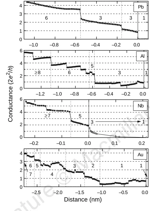
We have used various experimental methods to achieve stable atomic-size contacts: a scanning tunnelling microscope (STM) for the measurements on Pb (ref. 10), mechanically controllable break junctions for Nb (ref. 2), and lithographically fabricated versions of the latter (ref. 3) for Al and Au. Figure 1 shows the typical development of the conductance G for the four metals as the contacts are stretched. The total conductance decreases by steps until the contact breaks. After that it decreases exponentially with distance, the signature of the tunnel regime. The step heights are in the order ofG0, while the series of ‘‘plateaux’’ is different for each individual opening of the contact. It has been shown that the origin of the steps is in atomic rearrangements11–14which occur while the constriction is elongated. The typical value ofGat which the contact breaks, the lengths of the plateaux, and the behaviour within the plateaux are characteristic of each material. Pb shows plateaux with negative slope, and an almost continuous decrease ofGbetween 3G0and 1G0, where the contact usually breaks. Al has plateaux with positive slope, and breaks at aroundG0with a jump toG,0:1G0. Nb displays negatively inclined plateaux, smallest contacts with conductances between 2G0and 3G0, and a jump to a tunnelling conductance as high asG<G0. For our lithographic Au samples we obtain less well defined plateaux. The last contact before break typically has a conductance between 0.3G0and 0.8G0.
We can stop the elongation at any point and record the IVs. With the junction in the vacuum tunnel regime, the IV corresponds well to the one expected for a single channel as shown for Pb in curve e of Fig. 2. In the contact regime one observes IVs as depicted in curves a to d of the same figure. These curves were recorded on the same sample for different last plateaux before breaking. It is usually assumed that these smallest stable contacts are one-atom contacts2
. Our present analysis will give further support to this assumption. The occurrence of IVs with different sub-gap structure for the same total conductance (see Fig. 2) reveals the importance of the geo-metrical environment of the central atom for the conduction properties. In general, the IVs in the contact regime cannot be described by the single channel theory. We shall assume that the total current can be decomposed as:
IðVÞ ¼
^
N
n¼1
iðTn;VÞ ð1Þ
wherei(Tn,V) is the current of channeln. (This approximation is
justified as the multiple Andreev processes do not mix the normal conduction channels, see, for instance, ref. 15.) The solid curves in Fig. 2 are fits to the experimental IVs using equation (1), and the theoretical curvesi(T,V) calculated in ref. 8, with the set {Tn} and
the number of channels N as fitting parameters. Details of the analysis are given in ref. 5.
Nature © Macmillan Publishers Ltd 1998
8
letters to nature
NATURE|VOL 394|9 JULY 1998 155
than two channels are available,Gcan be well below 2G0. For larger contacts withG>3G0, we find six or more channels. The numbers Nof channels we found at the different plateaux are indicated in Fig. 1. Only channels with a transmission larger than 1% of the total transmission are taken into account when determiningN. Applying a similar analysis to different metals, we arrive at the important conclusion that the maximum number of channelsNmax for the smallest contacts is characteristic for a given metal. In the IVs of Al
smallest contacts we find typically the contributions of three channels, whereas for Nb we detect five channels. These results support our initial hypothesis thatNmaxfor one-atom contacts is limited by the number of valence orbitals of the central atomNorb.
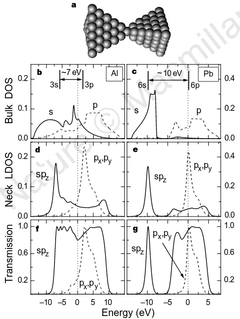
To gain insight into how the conduction channels are actually built up from the atomic orbital structure we have constructed a model of a one-atom constriction using an atomic orbital basis16,17. In references 16 and 17 it is explained in detail how the theoretical {Tn} can be obtained, and how the different atomic orbitals at the
central atom contribute to each conduction channel as a function of the atomic arrangement of the contact. Of course, the detailed atomic positions of the atoms in the experiments are unknown and quantitative comparison with theory is difficult. However, it turns out that the basic predictions of the model, in particular the number Nof conduction channels, are independent of the exact geometry chosen for the calculation. Figure 3 illustrates schematically the main results of our theoretical analysis for a one-atom contact between two closed packed pyramids (Fig. 3a) for Al (left) and Pb (right), for which one s orbital and three p orbitals have to be considered: due to the coupling of the central atom with its neighbours, the isolated atom’s energy levels (thick vertical bars in Fig. 3b and c) broaden to form a continuous local density of states (LDOS) in the neck (Fig. 3d and e). The central atom has less neighbours than an atom in the bulk material, and therefore the bands are narrower than deep inside the perfect crystal (Fig. 3b and c). In the neck geometry, the central-atom pz orbital (z is the
transport direction) splits off from the px and py orbitals and
hybridizes with the s orbital, building a channel of mixed spz
character. The actual transport properties of the atomic contact are determined by theTnvalues at the Fermi level EFwhich we determined self-consistently by imposing local charge neutrality (Fig. 3f and g)16,17.
For the perfectly ordered Pb contact the main predictions are: (1) three channels have a significantTnaround the Fermi energy, the
fourth one havingTn,10
23(not visible in Fig. 3); (2) the total transmission is close to 2.5 aroundEF, (3) there is one mode which is widely open for a broad energy range, and (4) the second transmis-sion eigenvalue is two-fold degenerate and has a smaller value –1.2 –1.0 –0.8 –0.6 –0.4 –0.2 0.0
0 2 4 6
Conductance (2
e
2
/h
)
1 3
5 6
≥8
–1.0 –0.8 –0.6 –0.4 –0.2 0.0 0
1 2 3 4
1 3 3
6
–0.2 –0.1 0.0 0.1 0.2
0 2 4 6
1
≥7 5
3
–2.5 –2.0 –1.5 –1.0 –0.5 0.0 0
1 2 3
4 Au
Nb Al Pb
1
7 6 5
Distance (nm)
1
4
2 3
Figure 1Typical conductanceGas a function of distance, recorded during a continuous opening of the samples, for four different metals. The distribution of transmission values{Tn}is established by fitting the IVs recorded at each point. The Pb data have been taken with a STM at 1.5 K. For preparing few-atom contacts with the STM, the Pb tip is indented repeatedly into the Pb sample surface and finally withdrawn10. For Al and Au we used lithographic break junctions below 100 mK. The initial samples before breaking are suspended nanobridges made of evaporated thin films with a central constrictions of about 200 nm3200 nm (ref. 3). The Nb data have been measured on a classical break junction, that is, a notched wire glued on top of a flexible substrate2, at 1.6 K. By bending the substrate the break junctions are elongated and finally broken. The opening speeds were in all cases in the range 1–10 pm s−1. The numbers indicate the numberNof conduction channels in each region. The symbol ‘‘$’’ means that only a lower bound forNcould be determined, because of systematic deviations from the theory due to a modified quasiparticle density of states (Nb) or because of experimental scattering (Al) which limits the maximumNthat can be disen-tangled. Plateaux corresponding to differentNare separated by dotted vertical lines. The horizontal arrow indicates thatNdecreases in the tunnel regime. Filled symbols indicate contact regime, open symbols the tunnel regime. The origins of the distance axes are arbitrarily set at the points where the contacts break. The distance scales for Al, Nb, and Au have been extracted from the exponential distance dependence of the current in the tunnel regime. The distance scale for the measurements on Pb has been determined using the calibration of the STM and is consistent with that deduced from the tunnel regime.
0 1 2 3
0
1 2 3 4
e d
c
b a
Current (
G
∆
/e
)
Voltage (
∆
/e)
Nature © Macmillan Publishers Ltd 1998
8
letters to nature
156 NATURE|VOL 394|9 JULY 1998
around EF. The widely open channel can be identified with the symmetric combination of s and pz. The two degenerate modes
mainly correspond to theporbitals perpendicular to thezdirection. The degeneracy of thepx,pymodes is due to the symmetry of the
perfectly ordered model geometry and is lifted when disorder is introduced. Furthermore, disorder slightly reduces the Tn of all
channels without altering the gross features16.
These predictions are in good agreement with our experimental observations: smallest Pb contacts just before breaking most fre-quently have aGbetween 1G0and 3G0. The decomposition usually results in three or four channels, where theTnof the fourth one, if
present, is usually smaller than 0.03. We do not find last plateaux before breaking with only one or two, or with five, channels. Typically the analysis of the last plateau yields one well transmitted mode withTn.0:6 and two smaller non-degenerate ones with
Tn<0:4. We attribute the lack of degeneracy and the smallerTns to
an asymmetrical environment around the central atom in the experimental contacts.
The case of Al is qualitatively similar because the relevant orbitals are of the same nature. However, the energy difference between the atomicsandplevels is smaller than in Pb. Furthermore, there are only three valence electrons and thereforeEFis lower. Our model predicts again three open channels for a perfect neck-shaped one-atom contact with a total conductance close toG0. Experimentally,
we obtain a last plateau withG0<G0, decomposable into three channels5. The case of an Al atom sandwiched between two flat surfaces has already been treated with density functional18and other ab initiocalculations19
, which predictedG<2G0.
For Nb one-atom contacts, Nmax¼6 as the density of states aroundEFis mainly determined by the contributions of one 5sand five 4dorbitals. The model calculations for Nb yield five channels with non-vanishingTn(ref. 16) adding up toG<2:8G0, again in
agreement with the experimental findings (see third panel of Fig. 1). The experimental determination of {Tn} is less precise than for Pb
and Al, because the quasiparticle density of states for Nb differs slightly from the one used for calculating thei(T,V). (Deviations of the quasiparticle density of states from the case considered in the theory mostly affect the shape of the current steps around V¼2∆=mebut not the current values in between. Therefore the analysis with the unmodified density of states is still possible.) An additional difference from the Pb and Al case is observed in the tunnel regime: for Nb contacts just after breaking, three channels contribute to the tunnel current. With increasing distance between the electrodes, one channel becomes dominating.
The cases discussed so far correspond to superconducting ele-ments having several valence orbitals per atom. A crucial test for the validity of our analysis would be provided by monovalent metals like Au and Na. They can be described by a singlesorbital, and the model predicts a single channel with T<1 for a one-atom contact16,17 in accordance with calculations based on molecular dynamics simulations20
. As these monovalent metals are not super-conducting, our method of characterizing channels is not directly applicable. However, a small piece of normal metal in good contact with a large piece of a superconductor develops a gap in its quasiparticle density of states21
. The lithographic mechanically controllable break junction technique3 allows for the fabrication of a constriction where the central region consists of Au atoms, embedded in a superconducting Al environment. Using shadow evaporation through a suspended mask we evaporated 400-nm-thick Al electrodes separated by a 50-nm-wide gap, which is filled with a 20-nm-thick Au layer deposited at a different angle under the same vacuum. The large asymmetry in thickness limits the influence of the normal metal on the quasiparticle density of states. As depicted in the lowermost panel of Fig. 1, we find indeed that the smallest Au contacts accommodate one single channel, contrary to the results for thesp-like and transition metals. However, we usually measure transmission values significantly below one. As for the other metals we interpret this reducedTwith respect to the model predictions as arising from disorder in the contact. Our Au samples are presumably more prone to disorder because of the very small Au layer thickness. Considering that the accuracy in determining {Tn} is
also limited because of the modified quasiparticle density of states, the single channel fit is still very satisfactory in the case of Au.
We draw two conclusions from our results. First, they provide clear evidence that the smallest contacts produced by the different experimental techniques are indeed one-atom contacts, asNnever exceeds Norb. We stress that in these experiments a single atom determines a macroscopic quantity, that is, the total conductance of the macroscopic circuit in which it is embedded. The current which an one-atom contact can sustain can be as large as 100mA, corresponding to the very large current density of 1011A cm−2. This large current is carried by a small number of conduction channels. Second, the ensemble of our experimental results shows unambiguously that the conduction channels in an atomic contact are determined by the chemical nature of the central atom. As a crude rule of thumb, the numberNof active channels corresponds to the number of valence electrons. This essential fact cannot be understood within a free electron model. Only a microscopic model that takes into account the atomic orbital structure as well as the local atomic geometry can fully explain the conduction properties of these contacts. We expect that these concepts will be applicable, in 0.0
0.1 0.2
sp
zd
px,py spz
px,py
Neck LDOS
0.0 0.2 0.4 e
10 eV ~
6p 6s
7 eV ~
3p 3s
–10 –5 0 5 10 0.2
0.6 1.0 f
px,py spz
Energy (eV)
Transmission
–10 –5 0 5 0.2 0.6 1.0 a
g
px,py
spz 0.0
0.1
0.2 b Al
p s
Bulk DOS
0.0 0.2 0.4 Pb c
p s
Figure 3Localized orbitals model for electrical conduction through one-atom contacts.a, Model geometry.b–g, Schematic development of the atomic valence levels (thick vertical bars inbandc) into bulk conduction bands (bandc) for Al and Pb. The panelsdandedepict schematically the local density of states (LDOS) in eV−1at the central atom of the model geometry. The global energy dependence of the transmission coefficientsTnis shown infandg. The dotted
lines indicate the position of the Fermi level. Thespzmode is the best transmitted
mode for both materials. The pxandpy modes are degenerate due to the
Nature © Macmillan Publishers Ltd 1998
8
letters to nature
NATURE|VOL 394|9 JULY 1998 157
slightly modified version, to conduction through clusters of atoms
and molecules. M
Received 29 December 1997; accepted 22 April 1998.
1. Crommie, M. F., Lutz, C. P. & Eigler, D. M. Confinement of electrons to quantum corrals on a metal surface.Science262,218–220 (1993).
2. van Ruitenbeek, J. M. inMesoscopic Electron Transport(eds Sohn, L. L., Kouwenhoven, L. P. & Scho¨n, G.) 549–579 (Kluwer Academic, Dordrecht, 1997).
3. van Ruitenbeek, J. M.et al. Adjustable nanofabricated atomic size contacts.Rev. Sci. Instrum.67,108– 111 (1996).
4. Landauer, R. Electrical resistance of disordered one-dimensional lattices.Phil. Mag.21,863–867 (1970).
5. Scheer, E., Joyez, P., Esteve, D., Urbina, C. & Devoret, M. H. Conduction channel transmissions of atomic-size aluminum contacts.Phys. Rev. Lett.78,3535–3538 (1997).
6. Octavio, M., Tinkham, M., Blonder, G. E. & Klapwijk, T. M. Subharmonic energy-gap structure in superconducting constrictions.Phys. Rev. B27,6739–6746 (1983).
7. Averin, D. & Bardas, A. AC Josephson effect in a single quantum channel.Phys. Rev. Lett.75,1831– 1834 (1995).
8. Cuevas, J. C., Martı´n-Rodero, A. & Levy Yeyati, A. Hamiltonian approach to the transport properties of superconducting quantum point contacts.Phys. Rev. B54,7366–7379 (1996).
9. Bratus, E. N., Shumeiko, V. S., Bezuglyi, E. V. & Wendin, G. dc-current transport and ac Josephson effect in quantum junctions at low voltage.Phys. Rev. B55,12666–12677 (1997).
10. Agraı¨t, N., Rodrigo, J. G. & Vieira, S. Conductance steps and quantization in atomic-size contacts.
Phys. Rev. B47,12345–12348 (1996).
11. Rubio, G., Agraı¨t, N. & Vieira, S. Atomic-sized metallic contacts: mechanical properties and electronic transport.Phys. Rev. Lett.76,2302–2305 (1996).
12. Krans, J. M., van Ruitenbeek, J. M., Fisun, V. V., Yanson, I. K. & de Jongh, L. J. The signature of conductance quantization in metallic point contacts.Nature375,767–769 (1995).
13. Landman, U., Luedtke, W. D., Salisbury, B. E. & Whetten, R. L. Reversible manipulations of room temperature mechanical and quantum transport properties in nanowire junctions.Phys. Rev. Lett.77, 1362–1365 (1996).
14. Todorov, T. N. & Sutton, A. P. Jumps in electronic conductance due to mechanical instabilities.Phys. Rev. Lett.70,2138–2141 (1993).
15. Beenakker, C. W. J. Quantum transport in semiconductor superconductor microjunctions.Phys. Rev. B46,12841–12844 (1992).
16. Cuevas, J. C., Levy Yeyati, A. & Martı´n-Rodero, A. Microscopic origin of the conducting channels in metallic atomic-size contacts.Phys. Rev. Lett.80,1066–1069 (1998).
17. Levy Yeyati, A., Martı´n-Rodero, A. & Flores, F. Conductance quantization and electron resonances in sharp tips and atomic size contacts.Phys. Rev. B56,10369–10372 (1997).
18. Lang, N. D. Resistance of atomic wires.Phys. Rev. B52,5335–5342 (1995).
19. Wan, C. C., Mozos, J.-L., Taraschi, G., Wang, J. & Guo, H. Quantum transport through atomic wires.
Appl. Phys. Lett.71,419–421 (1997).
20. Brandbyge, M., Sørensen, M. R. & Jacobsen, K. W. Conductance eigenchannels in nanocontacts.Phys. Rev. B56,14956–14959 (1997).
21. Belzig, W., Bruder, C. & Scho¨n, G. Local density of states in a dirty normal metal connected to a superconductor.Phys. Rev. B54,9443–9448 (1996).
Acknowledgements.We thank D. Esteve and M. H. Devoret for discussions and C. Su¨rgers for graphics preparation; N.A. and G.R.B. thank S. Vieira for discussions and support. The work was supported in part by the Deutsche Forschungsgemeinschaft (DFG), the Spanish CICYT, ‘‘Stichting FOM’’ (NWO) and the Bureau National de Me´trologie (BNM).
Correspondence and requests for materials should be addressed to E.S. (e-mail: Elke.Scheer@ phys.uni-karlsruhe.de).
Cation effects in doped
La
2
CuO
4
superconductors
J. P. Attfield, A. L. Kharlanov*& J. A. McAllister*
Interdisciplinary Research Centre in Superconductivity, University of Cambridge, Madingley Road, Cambridge CB3 OHE, UK, and Department of Chemistry, University of Cambridge, Lensfield Road, Cambridge CB2 1EW, UK *These authors contributed equally to the work
. . . .
The critical temperatures of (Ln1−xMx)2CuO4superconductors 1, in
which Ln3+(La and other lanthanides) and M2+(Ca, Sr, Ba) cations are randomly distributed amongst the ‘type A’ lattice sites, are known to depend on the doping level, x, and the mean A-site
cation radius,hrAi(refs 2, 3). Here we show, by studying series of
compositions with the same doping level andhrAi, that the critical
temperature decreases linearly with increasing A-site disorder, as quantified by the variance in the distribution of A-site cation radii. From this, we are able to show that, in the absence of disorder, the critical temperature should increase quadratically withhrAifor superconductors containing a single CuO2layer. Our
results therefore show that the critical temperature is very sensitive to lattice strains, as has also been shown for the metal to insulator transition temperature in the magnetoresistive (Ln1−xMx)MnO3perovskites
4.
Study of a series of (Ln0.7M0.3)MnO3perovskites in which the mean A-site cation radiushrAiwas held constant has showed4that the metal–insulator transition temperatureTmdecreases linearly with the statistical variancej2in the distribution of A-site radii5, j2
¼hr2 Ai2hrAi
2
. The hole-doped (Ln1−xMx)2CuO4superconductors
are similar to the above perovskites in that the doping level and lattice effects are controlled by the Ln3+and M2+cations at the A-sites, which in this case are adjacent to two-dimensional CuO2perovskite layers. Many compositions with the ‘optimum’ doping level x¼0:075, which maximizes the superconducting critical tempera-tureTcin the (La1−xSrx)2CuO4system6, have been reported, and the
variation ofTcwithhrAifor series of (La0.925Sr0.075−xBax)2CuO4(ref. 7)
and (La0.925−xLnxSr0.075)2CuO4 (Ln¼Pr, Nd, Sm, Eu)3,8
com-positions are shown in Fig. 1. Systematic changes with a maximum TcathrAi¼1:22 ˚A are observed, butTcis not uniquely determined byhrAiat the given doping level.
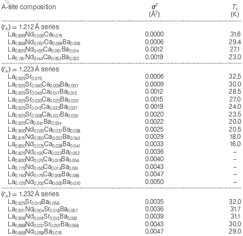
To determine whether Tc is sensitive to A-site disorder, we have prepared three series of (La0.925−fNdfSr0.075−g−hCagBah)2CuO4
compositions with the fixed x¼0:075 doping level (Table 1). Values ofhrAiandj2were calculated from reported ionic radii for nine-coordination5
. Initially, 15 compositions were prepared with hrAi¼1:223 ˚A, the value for (La0.925Sr0.075)2CuO4(thef ¼g¼h¼0 composition). The A-cation size disorder varies between
Table 1 Properties of three A2CuO4series with fixed mean A-site radius
A-site composition j2
(A˚2) (K)Tc
...
hrAi¼1:212A series˚
La0.899Nd0.026Ca0.075 0.0000 31.6
La0.868Nd0.057Ca0.069Ba0.006 0.0006 29.4
La0.825Nd0.100Ca0.061Ba0.014 0.0012 27.1
La0.781Nd0.144Ca0.053Ba0.022 0.0019 23.0
...
hrAi¼1:223A series˚
La0.925Sr0.075 0.0006 32.5
La0.925Sr0.060Ca0.008Ba0.007 0.0009 30.0
La0.925Sr0.045Ca0.017Ba0.013 0.0012 28.5
La0.925Sr0.030Ca0.025Ba0.020 0.0015 27.0
La0.925Sr0.015Ca0.033Ba0.027 0.0019 24.0
La0.925Sr0.008Ca0.037Ba0.030 0.0020 23.5
La0.925Ca0.041Ba0.034 0.0022 20.0
La0.900Nd0.025Ca0.037Ba0.038 0.0025 20.5
La0.875Nd0.050Ca0.032Ba0.043 0.0029 18.0
La0.850Nd0.075Ca0.028Ba0.047 0.0033 16.0
La0.825Nd0.100Ca0.023Ba0.052 0.0036 —
La0.800Nd0.125Ca0.019Ba0.056 0.0040 —
La0.775Nd0.150Ca0.014Ba0.061 0.0043 —
La0.750Nd0.175Ca0.009Ba0.066 0.0047 —
La0.725Nd0.200Ca0.005Ba0.070 0.0050 —
...
hrAi¼1:232A series˚
La0.925Sr0.019Ba0.056 0.0035 32.0
La0.921Nd0.004Sr0.018Ba0.057 0.0036 31.7
La0.906Nd0.019Sr0.013Ba0.062 0.0039 31.1
La0.888Nd0.037Sr0.007Ba0.068 0.0043 30.0
La0.868Nd0.058Ba0.075 0.0047 29.0
...
Herej2is the cation size variance, andhr
Aiis the fixed mean A-site radius. A dash in the
rightmost column indicates that superconductivity was not detected.
10 15 20 25 30 35 40
T
(K)
1.20 1.21 1.22 1.23 1.24
c
A
<r > (Å)