SEVENTH EDITION
E
LECTRONIC
D
EVICES
AND
C
IRCUIT
T
HEORY
ROBERT BOYLESTAD
LOUIS NASHELSKY
PRENTICE HALL
Contents
v
PREFACE
xiii
ACKNOWLEDGMENTS
xvii
1
SEMICONDUCTOR DIODES
1
1.1 Introduction 1 1.2 Ideal Diode 1
1.3 Semiconductor Materials 3 1.4 Energy Levels 6
1.5 Extrinsic Materials—n- and p-Type 7
1.6 Semiconductor Diode 10 1.7 Resistance Levels 17
1.8 Diode Equivalent Circuits 24 1.9 Diode Specification Sheets 27
1.10 Transition and Diffusion Capacitance 31 1.11 Reverse Recovery Time 32
1.12 Semiconductor Diode Notation 32 1.13 Diode Testing 33
1.14 Zener Diodes 35
1.15 Light-Emitting Diodes (LEDs) 38 1.16 Diode Arrays—Integrated Circuits 42 1.17 PSpice Windows 43
2
DIODE APPLICATIONS
51
2.4 Series Diode Configurations with DC Inputs 59 2.5 Parallel and Series-Parallel Configurations 64 2.6 AND/OR Gates 67
2.7 Sinusoidal Inputs; Half-Wave Rectification 69 2.8 Full-Wave Rectification 72
2.9 Clippers 76 2.10 Clampers 83 2.11 Zener Diodes 87
2.12 Voltage-Multiplier Circuits 94 2.13 PSpice Windows 97
3
BIPOLAR JUNCTION TRANSISTORS
112
3.1 Introduction 112
3.2 Transistor Construction 113 3.3 Transistor Operation 113
3.4 Common-Base Configuration 115 3.5 Transistor Amplifying Action 119 3.6 Common-Emitter Configuration 120 3.7 Common-Collector Configuration 127 3.8 Limits of Operation 128
3.9 Transistor Specification Sheet 130 3.10 Transistor Testing 134
3.11 Transistor Casing and Terminal Identification 136 3.12 PSpice Windows 138
4
DC BIASING—BJTS
143
4.1 Introduction 143 4.2 Operating Point 144 4.3 Fixed-Bias Circuit 146
4.4 Emitter-Stabilized Bias Circuit 153 4.5 Voltage-Divider Bias 157
4.6 DC Bias with Voltage Feedback 165 4.7 Miscellaneous Bias Configurations 168 4.8 Design Operations 174
4.9 Transistor Switching Networks 180 4.10 Troubleshooting Techniques 185 4.11 PNP Transistors 188
4.12 Bias Stabilization 190 4.13 PSpice Windows 199
5
FIELD-EFFECT TRANSISTORS
211
5.1 Introduction 211
5.4 Specification Sheets (JFETs) 223 5.5 Instrumentation 226
5.6 Important Relationships 227 5.7 Depletion-Type MOSFET 228 5.8 Enhancement-Type MOSFET 234 5.9 MOSFET Handling 242
5.10 VMOS 243 5.11 CMOS 244
5.12 Summary Table 246 5.13 PSpice Windows 247
6
FET BIASING
253
6.1 Introduction 253
6.2 Fixed-Bias Configuration 254 6.3 Self-Bias Configuration 258 6.4 Voltage-Divider Biasing 264 6.5 Depletion-Type MOSFETs 270 6.6 Enhancement-Type MOSFETs 274 6.7 Summary Table 280
6.8 Combination Networks 282 6.9 Design 285
6.10 Troubleshooting 287 6.11 P-Channel FETs 288
6.12 Universal JFET Bias Curve 291 6.13 PSpice Windows 294
7
BJT TRANSISTOR MODELING
305
7.1 Introduction 305
7.2 Amplification in the AC Domain 305 7.3 BJT Transistor Modeling 306
7.4 The Important Parameters: Zi, Zo, Av, Ai 308
7.5 The reTransistor Model 314
7.6 The Hybrid Equivalent Model 321
7.7 Graphical Determination of the h-parameters 327
7.8 Variations of Transistor Parameters 331
8
BJT SMALL-SIGNAL ANALYSIS
338
8.1 Introduction 338
8.3 Common-Emitter Fixed-Bias Configuration 338 8.3 Voltage-Divider Bias 342
8.4 CE Emitter-Bias Configuration 345 8.3 Emitter-Follower Configuration 352 8.6 Common-Base Configuration 358
vii
8.7 Collector Feedback Configuration 360 8.8 Collector DC Feedback Configuration 366 8.9 Approximate Hybrid Equivalent Circuit 369 8.10 Complete Hybrid Equivalent Model 375 8.11 Summary Table 382
8.12 Troubleshooting 382 8.13 PSpice Windows 385
9
FET SMALL-SIGNAL ANALYSIS
401
9.1 Introduction 401
9.2 FET Small-Signal Model 402 9.3 JFET Fixed-Bias Configuration 410 9.4 JFET Self-Bias Configuration 412 9.5 JFET Voltage-Divider Configuration 418
9.6 JFET Source-Follower (Common-Drain) Configuration 419 9.7 JFET Common-Gate Configuration 422
9.8 Depletion-Type MOSFETs 426 9.9 Enhancement-Type MOSFETs 428
9.10 E-MOSFET Drain-Feedback Configuration 429 9.11 E-MOSFET Voltage-Divider Configuration 432 9.12 Designing FET Amplifier Networks 433 9.13 Summary Table 436
9.14 Troubleshooting 439 9.15 PSpice Windows 439
10
SYSTEMS APPROACH—
EFFECTS OF
R
sAND
R
L452
10.1 Introduction 452 10.2 Two-Port Systems 452
10.3 Effect of a Load Impedance (RL) 454
10.4 Effect of a Source Impedance (Rs) 459
10.5 Combined Effect of Rsand RL 461
10.6 BJT CE Networks 463
10.7 BJT Emitter-Follower Networks 468 10.8 BJT CB Networks 471
10.9 FET Networks 473 10.10 Summary Table 476 10.11 Cascaded Systems 480 10.12 PSpice Windows 481
11
BJT AND JFET FREQUENCY RESPONSE
493
11.4 General Frequency Considerations 500 11.5 Low-Frequency Analysis—Bode Plot 503 11.6 Low-Frequency Response—BJT Amplifier 508 11.7 Low-Frequency Response—FET Amplifier 516 11.8 Miller Effect Capacitance 520
11.9 High-Frequency Response—BJT Amplifier 523 11.10 High-Frequency Response—FET Amplifier 530 11.11 Multistage Frequency Effects 534
11.12 Square-Wave Testing 536 11.13 PSpice Windows 538
12
COMPOUND CONFIGURATIONS
544
12.1 Introduction 544
12.2 Cascade Connection 544 12.3 Cascode Connection 549 12.4 Darlington Connection 550 12.5 Feedback Pair 555
12.6 CMOS Circuit 559
12.7 Current Source Circuits 561 12.8 Current Mirror Circuits 563 12.9 Differential Amplifier Circuit 566
12.10 BIFET, BIMOS, and CMOS Differential Amplifier Circuits 574 12.11 PSpice Windows 575
13
DISCRETE AND IC
MANUFACTURING TECHNIQUES
588
13.1 Introduction 588
13.2 Semiconductor Materials, Si, Ge, and GaAs 588 13.3 Discrete Diodes 590
13.4 Transistor Fabrication 592 13.5 Integrated Circuits 593
13.6 Monolithic Integrated Circuit 595 13.7 The Production Cycle 597
13.8 Thin-Film and Thick-Film Integrated Circuits 607 13.9 Hybrid Integrated Circuits 608
14
OPERATIONAL AMPLIFIERS
609
14.1 Introduction 609
14.2 Differential and Common-Mode Operation 611 14.3 Op-Amp Basics 615
14.4 Practical Op-Amp Circuits 619
14.5 Op-Amp Specifications—DC Offset Parameters 625 14.6 Op-Amp Specifications—Frequency Parameters 628 14.7 Op-Amp Unit Specifications 632
14.8 PSpice Windows 638
ix
15
OP-AMP APPLICATIONS
648
15.1 Constant-Gain Multiplier 648 15.2 Voltage Summing 652 15.3 Voltage Buffer 655 15.4 Controller Sources 656 15.5 Instrumentation Circuits 658 15.6 Active Filters 662
15.7 PSpice Windows 666
16
POWER AMPLIFIERS
679
16.1 Introduction—Definitions and Amplifier Types 679 16.2 Series-Fed Class A Amplifier 681
16.3 Transformer-Coupled Class A Amplifier 686 16.4 Class B Amplifier Operation 693
16.5 Class B Amplifier Circuits 697 16.6 Amplifier Distortion 704
16.7 Power Transistor Heat Sinking 708 16.8 Class C and Class D Amplifiers 712 16.9 PSpice Windows 714
17
LINEAR-DIGITAL ICs
721
17.1 Introduction 721
17.2 Comparator Unit Operation 721 17.3 Digital-Analog Converters 728 17.4 Timer IC Unit Operation 732 17.5 Voltage-Controlled Oscillator 735 17.6 Phase-Locked Loop 738
17.7 Interfacing Circuitry 742 17.8 PSpice Windows 745
18
FEEDBACK AND OSCILLATOR CIRCUITS
751
18.1 Feedback Concepts 751
18.2 Feedback Connection Types 752 18.3 Practical Feedback Circuits 758
18.4 Feedback Amplifier—Phase and Frequency Considerations 765 18.5 Oscillator Operation 767
19
POWER SUPPLIES
(VOLTAGE REGULATORS)
783
19.1 Introduction 783
19.2 General Filter Considerations 783 19.3 Capacitor Filter 786
19.4 RC Filter 789
19.5 Discrete Transistor Voltage Regulation 792 19.6 IC Voltage Regulators 799
19.7 PSpice Windows 804
20
OTHER TWO-TERMINAL DEVICES
810
20.1 Introduction 810
20.2 Schottky Barrier (Hot-Carrier) Diodes 810 20.3 Varactor (Varicap) Diodes 814
20.4 Power Diodes 818 20.5 Tunnel Diodes 819 20.6 Photodiodes 824
20.7 Photoconductive Cells 827 20.8 IR Emitters 829
20.9 Liquid-Crystal Displays 831 20.10 Solar Cells 833
20.11 Thermistors 837
21
pnpn
AND OTHER DEVICES
842
21.1 Introduction 842
21.2 Silicon-Controlled Rectifier 842
21.3 Basic Silicon-Controlled Rectifier Operation 842 21.4 SCR Characteristics and Ratings 845
21.5 SCR Construction and Terminal Identification 847 21.6 SCR Applications 848
21.7 Silicon-Controlled Switch 852 21.8 Gate Turn-Off Switch 854 21.9 Light-Activated SCR 855 21.10 Shockley Diode 858 21.11 DIAC 858
21.12 TRIAC 860
21.13 Unijunction Transistor 861 21.14 Phototransistors 871 21.15 Opto-Isolators 873
21.16 Programmable Unijunction Transistor 875
xi
22
OSCILLOSCOPE AND OTHER
MEASURING INSTRUMENTS
884
22.1 Introduction 884
22.2 Cathode Ray Tube—Theory and Construction 884 22.3 Cathode Ray Oscilloscope Operation 885
22.4 Voltage Sweep Operation 886 22.5 Synchronization and Triggering 889 22.6 Multitrace Operation 893
22.7 Measurement Using Calibrated CRO Scales 893 22.8 Special CRO Features 898
22.9 Signal Generators 899
APPENDIX A: HYBRID PARAMETERS—
CONVERSION EQUATIONS
(EXACT AND APPROXIMATE)
902
APPENDIX B: RIPPLE FACTOR AND
VOLTAGE CALCULATIONS
904
APPENDIX C: CHARTS AND TABLES
911
APPENDIX D: SOLUTIONS TO SELECTED
ODD-NUMBERED PROBLEMS
913
Acknowledgments
Our sincerest appreciation must be extended to the instructors who have used the text and sent in comments, corrections, and suggestions. We also want to thank Rex David-son, Production Editor at Prentice Hall, for keeping together the many detailed as-pects of production. Our sincerest thanks to Dave Garza, Senior Editor, and Linda Ludewig, Editor, at Prentice Hall for their editorial support of the Seventh Edition of this text.
We wish to thank those individuals who have shared their suggestions and evalua-tions of this text throughout its many edievalua-tions. The comments from these individu-als have enabled us to present Electronic Devices and Circuit Theory in this Seventh
Edition:
Ernest Lee Abbott Napa College, Napa, CA
Phillip D. Anderson Muskegon Community College, Muskegon, MI
Al Anthony EG&G VACTEC Inc.
A. Duane Bailey Southern Alberta Institute of Technology, Calgary, Alberta, CANADA
Joe Baker University of Southern California, Los Angeles, CA
Jerrold Barrosse Penn State–Ogontz
Ambrose Barry University of North Carolina–Charlotte
Arthur Birch Hartford State Technical College, Hartford, CT
Scott Bisland SEMATECH, Austin, TX
Edward Bloch The Perkin-Elmer Corporation
Gary C. Bocksch Charles S. Mott Community College, Flint, MI
Jeffrey Bowe Bunker Hill Community College, Charlestown, MA
Alfred D. Buerosse Waukesha County Technical College, Pewaukee, WI
Lila Caggiano MicroSim Corporation
Mauro J. Caputi Hofstra University
Robert Casiano International Rectifier Corporation
Alan H. Czarapata Montgomery College, Rockville, MD
Mohammad Dabbas ITT Technical Institute
John Darlington Humber College, Ontario, CANADA
Lucius B. Day Metropolitan State College, Denver, CO
Mike Durren Indiana Vocational Technical College, South Bend, IN
Dr. Stephen Evanson Bradford University, UK
George Fredericks Northeast State Technical Community College, Blountville, TN
F. D. Fuller Humber College, Ontario, CANADA
Phil Golden DeVry Institute of Technology, Irving, TX
Joseph Grabinski Hartford State Technical College, Hartfold, CT
Thomas K. Grady Western Washington University, Bellingham, WA
William Hill ITT Technical Institute
Albert L. Ickstadt San Diego Mesa College, San Diego, CA
Jeng-Nan Juang Mercer University, Macon, GA
Karen Karger Tektronix Inc.
Kenneth E. Kent DeKalb Technical Institute, Clarkston, GA
Donald E. King ITT Technical Institute, Youngstown, OH
Charles Lewis APPLIED MATERIALS, INC.
Donna Liverman Texas Instruments Inc.
William Mack Harrisburg Area Community College
Robert Martin Northern Virginia Community College
George T. Mason Indiana Vocational Technical College, South Bend, IN
William Maxwell Nashville State Technical Institute
Abraham Michelen Hudson Valley Community College
John MacDougall University of Western Ontario, London, Ontario, CANADA
Donald E. McMillan Southwest State University, Marshall, MN
Thomas E. Newman L. H. Bates Vocational-Technical Institute, Tacoma, WA
Byron Paul Bismarck State College
Dr. Robert Payne University of Glamorgan, Wales, UK
Dr. Robert A. Powell Oakland Community College
E. F. Rockafellow Southern-Alberta Institute of Technology, Calgary, Alberta, CANADA
Saeed A. Shaikh Miami-Dade Community College, Miami, FL
Dr. Noel Shammas School of Engineering, Beaconside, UK
Ken Simpson Stark State College of Technology
Eric Sung Computronics Technology Inc.
Donald P. Szymanski Owens Technical College, Toledo, OH
Parker M. Tabor Greenville Technical College, Greenville, SC
Peter Tampas Michigan Technological University, Houghton, MI
Chuck Tinney University of Utah
Katherine L. Usik Mohawk College of Applied Art & Technology, Hamilton, Ontario, CANADA
Domingo Uy Hampton University, Hampton, VA
Richard J. Walters DeVry Technical Institute, Woodbridge, NJ
Larry J. Wheeler PSE&G Nuclear
Julian Wilson Southern College of Technology, Marietta, GA
Syd R. Wilson Motorola Inc.
Jean Younes ITT Technical Institute, Troy, MI
Charles E. Yunghans Western Washington University, Bellingham, WA
p n
C H A P T E R
1
Semiconductor
Diodes
1.1
INTRODUCTION
It is now some 50 years since the first transistor was introduced on December 23, 1947. For those of us who experienced the change from glass envelope tubes to the solid-state era, it still seems like a few short years ago. The first edition of this text contained heavy coverage of tubes, with succeeding editions involving the important decision of how much coverage should be dedicated to tubes and how much to semi-conductor devices. It no longer seems valid to mention tubes at all or to compare the advantages of one over the other—we are firmly in the solid-state era.
The miniaturization that has resulted leaves us to wonder about its limits. Com-plete systems now appear on wafers thousands of times smaller than the single ele-ment of earlier networks. New designs and systems surface weekly. The engineer be-comes more and more limited in his or her knowledge of the broad range of advances— it is difficult enough simply to stay abreast of the changes in one area of research or development. We have also reached a point at which the primary purpose of the con-tainer is simply to provide some means of handling the device or system and to pro-vide a mechanism for attachment to the remainder of the network. Miniaturization appears to be limited by three factors (each of which will be addressed in this text): the quality of the semiconductor material itself, the network design technique, and the limits of the manufacturing and processing equipment.
1.2
IDEAL DIODE
The first electronic device to be introduced is called the diode.It is the simplest of
semiconductor devices but plays a very vital role in electronic systems, having char-acteristics that closely match those of a simple switch. It will appear in a range of ap-plications, extending from the simple to the very complex. In addition to the details of its construction and characteristics, the very important data and graphs to be found on specification sheets will also be covered to ensure an understanding of the termi-nology employed and to demonstrate the wealth of information typically available from manufacturers.
The term idealwill be used frequently in this text as new devices are introduced.
It refers to any device or system that has ideal characteristics—perfect in every way. It provides a basis for comparison, and it reveals where improvements can still be made. The ideal diode is a two-terminal device having the symbol and
characteris-tics shown in Figs. 1.1a and b, respectively.
1
Figure 1.1 Ideal diode: (a)
Ideally, a diode will conduct current in the direction defined by the arrow in the symbol and act like an open circuit to any attempt to establish current in the oppo-site direction. In essence:
The characteristics of an ideal diode are those of a switch that can conduct current in only one direction.
In the description of the elements to follow, it is critical that the various letter symbols, voltage polarities, and current directions be defined. If the polarity of the
applied voltage is consistent with that shown in Fig. 1.1a, the portion of the charac-teristics to be considered in Fig. 1.1b is to the right of the vertical axis. If a reverse voltage is applied, the characteristics to the left are pertinent. If the current through the diode has the direction indicated in Fig. 1.1a, the portion of the characteristics to be considered is above the horizontal axis, while a reversal in direction would require the use of the characteristics below the axis. For the majority of the device charac-teristics that appear in this book, the ordinate(or “y” axis) will be the currentaxis,
while the abscissa(or “x” axis) will be the voltage axis.
One of the important parameters for the diode is the resistance at the point or re-gion of operation. If we consider the conduction rere-gion defined by the direction of ID
and polarity of VDin Fig. 1.1a (upper-right quadrant of Fig. 1.1b), we will find that
the value of the forward resistance,RF, as defined by Ohm’s law is
RF V
IF
F
0 ⍀ (short circuit)
where VFis the forward voltage across the diode and IFis the forward current through
the diode.
The ideal diode, therefore, is a short circuit for the region of conduction.
Consider the region of negatively applied potential (third quadrant) of Fig. 1.1b,
RR V
IR R
ⴥ ⍀ (open-circuit)
where VR is reverse voltage across the diode and IR is reverse current in the diode. The ideal diode, therefore, is an open circuit in the region of nonconduction.
In review, the conditions depicted in Fig. 1.2 are applicable.
5,20, or any reverse-bias potential
0 mA 0 V
2, 3, mA, . . . , or any positive value
Figure 1.2 (a) Conduction and (b) nonconduction states of the ideal diode as
determined by the applied bias.
D
V
– +
D
V
+ –
D
I
0 D
I
D
V
= 0
(limited by circuit)
Open circuit Short circuit
(a)
(b) D
I
In general, it is relatively simple to determine whether a diode is in the region of conduction or nonconduction simply by noting the direction of the current ID
3
the resulting current has the opposite direction, as shown in Fig. 1.3b, the open-circuit equivalent is appropriate.
1.3 Semiconductor Materials
Figure 1.3 (a) Conduction
and (b) nonconduction states of the ideal diode as determined by the direction of conventional current established by the network.
D
I = 0
(b) D
I
D
I ID
(a)
As indicated earlier, the primary purpose of this section is to introduce the char-acteristics of an ideal device for comparison with the charchar-acteristics of the commer-cial variety. As we progress through the next few sections, keep the following ques-tions in mind:
How close will the forward or “on” resistance of a practical diode compare with the desired 0- level?
Is the reverse-bias resistance sufficiently large to permit an open-circuit ap-proximation?
1.3
SEMICONDUCTOR MATERIALS
The label semiconductoritself provides a hint as to its characteristics. The prefix
semi-is normally applied to a range of levels midway between two limits.
The term conductor is applied to any material that will support a generous flow of charge when a voltage source of limited magnitude is applied across its terminals.
An insulator is a material that offers a very low level of conductivity under pressure from an applied voltage source.
A semiconductor, therefore, is a material that has a conductivity level some-where between the extremes of an insulator and a conductor.
Inversely related to the conductivity of a material is its resistance to the flow of charge, or current. That is, the higher the conductivity level, the lower the resistance level. In tables, the term resistivity(, Greek letter rho) is often used when
compar-ing the resistance levels of materials. In metric units, the resistivity of a material is measured in -cm or -m. The units of -cm are derived from the substitution of
the units for each quantity of Fig. 1.4 into the following equation (derived from the basic resistance equation Rl/A):
R
l A
()
c ( m cm2)
⇒-cm (1.1)
In fact, if the area of Fig. 1.4 is 1 cm2and the length 1 cm, the magnitude of the
resistance of the cube of Fig. 1.4 is equal to the magnitude of the resistivity of the material as demonstrated below:
R
A l
( (
1 1
c c
m m
2
) )
ohms
This fact will be helpful to remember as we compare resistivity levels in the discus-sions to follow.
In Table 1.1, typical resistivity values are provided for three broad categories of materials. Although you may be familiar with the electrical properties of copper and
Figure 1.4 Defining the metric
TABLE 1.1 Typical Resistivity Values
Conductor Semiconductor Insulator
⬵106-cm ⬵50 -cm (germanium) ⬵1012-cm
(copper) ⬵50103-cm (silicon) (mica)
mica from your past studies, the characteristics of the semiconductor materials of ger-manium (Ge) and silicon (Si) may be relatively new. As you will find in the chapters to follow, they are certainly not the only two semiconductor materials. They are, how-ever, the two materials that have received the broadest range of interest in the devel-opment of semiconductor devices. In recent years the shift has been steadily toward silicon and away from germanium, but germanium is still in modest production.
Note in Table 1.1 the extreme range between the conductor and insulating mate-rials for the 1-cm length (1-cm2area) of the material. Eighteen places separate the
placement of the decimal point for one number from the other. Ge and Si have re-ceived the attention they have for a number of reasons. One very important consid-eration is the fact that they can be manufactured to a very high purity level. In fact, recent advances have reduced impurity levels in the pure material to 1 part in 10 bil-lion (1⬊10,000,000,000). One might ask if these low impurity levels are really
nec-essary. They certainly are if you consider that the addition of one part impurity (of the proper type) per million in a wafer of silicon material can change that material from a relatively poor conductor to a good conductor of electricity. We are obviously dealing with a whole new spectrum of comparison levels when we deal with the semi-conductor medium. The ability to change the characteristics of the material signifi-cantly through this process, known as “doping,” is yet another reason why Ge and Si have received such wide attention. Further reasons include the fact that their charac-teristics can be altered significantly through the application of heat or light—an im-portant consideration in the development of heat- and light-sensitive devices.
Some of the unique qualities of Ge and Si noted above are due to their atomic structure. The atoms of both materials form a very definite pattern that is periodic in nature (i.e., continually repeats itself). One complete pattern is called a crystaland
the periodic arrangement of the atoms a lattice. For Ge and Si the crystal has the
three-dimensional diamond structure of Fig. 1.5. Any material composed solely of re-peating crystal structures of the same kind is called a single-crystal structure. For
semiconductor materials of practical application in the electronics field, this single-crystal feature exists, and, in addition, the periodicity of the structure does not change significantly with the addition of impurities in the doping process.
Let us now examine the structure of the atom itself and note how it might affect the electrical characteristics of the material. As you are aware, the atom is composed of three basic particles: the electron,the proton, and the neutron.In the atomic
lat-tice, the neutrons and protons form the nucleus, while the electrons revolve around
the nucleus in a fixed orbit.The Bohr models of the two most commonly used
semi-conductors,germaniumand silicon,are shown in Fig. 1.6.
As indicated by Fig. 1.6a, the germanium atom has 32 orbiting electrons, while silicon has 14 orbiting electrons. In each case, there are 4 electrons in the outermost (valence) shell. The potential (ionization potential) required to remove any one of
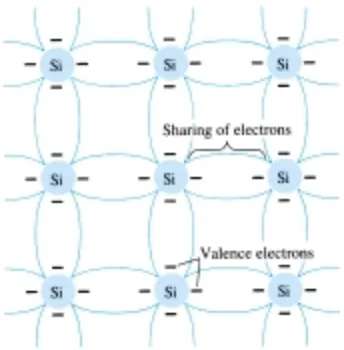
these 4 valence electrons is lower than that required for any other electron in the struc-ture. In a pure germanium or silicon crystal these 4 valence electrons are bonded to 4 adjoining atoms, as shown in Fig. 1.7 for silicon. Both Ge and Si are referred to as
tetravalent atomsbecause they each have four valence electrons.
A bonding of atoms, strengthened by the sharing of electrons, is called cova-lent bonding.
Figure 1.5 Ge and Si
5
Although the covalent bond will result in a stronger bond between the valence electrons and their parent atom, it is still possible for the valence electrons to absorb sufficient kinetic energy from natural causes to break the covalent bond and assume the “free” state. The term freereveals that their motion is quite sensitive to applied
electric fields such as established by voltage sources or any difference in potential. These natural causes include effects such as light energy in the form of photons and thermal energy from the surrounding medium. At room temperature there are approx-imately 1.51010free carriers in a cubic centimeter of intrinsic silicon material.
Intrinsic materials are those semiconductors that have been carefully refined to reduce the impurities to a very low level—essentially as pure as can be made available through modern technology.
The free electrons in the material due only to natural causes are referred to as
intrinsic carriers.At the same temperature, intrinsic germanium material will have
approximately 2.51013free carriers per cubic centimeter. The ratio of the
num-ber of carriers in germanium to that of silicon is greater than 103 and would
indi-cate that germanium is a better conductor at room temperature. This may be true, but both are still considered poor conductors in the intrinsic state. Note in Table 1.1 that the resistivity also differs by a ratio of about 1000⬊1, with silicon having the
larger value. This should be the case, of course, since resistivity and conductivity are inversely related.
An increase in temperature of a semiconductor can result in a substantial in-crease in the number of free electrons in the material.
As the temperature rises from absolute zero (0 K), an increasing number of va-lence electrons absorb sufficient thermal energy to break the covalent bond and con-tribute to the number of free carriers as described above. This increased number of carriers will increase the conductivity index and result in a lower resistance level.
Semiconductor materials such as Ge and Si that show a reduction in resis-tance with increase in temperature are said to have a negative temperature coefficient.
You will probably recall that the resistance of most conductors will increase with temperature. This is due to the fact that the numbers of carriers in a conductor will
1.3 Semiconductor Materials
Figure 1.6 Atomic structure: (a) germanium;
(b) silicon.
Figure 1.7 Covalent bonding of the silicon
not increase significantly with temperature, but their vibration pattern about a rela-tively fixed location will make it increasingly difficult for electrons to pass through. An increase in temperature therefore results in an increased resistance level and a pos-itive temperature coefficient.
1.4
ENERGY LEVELS
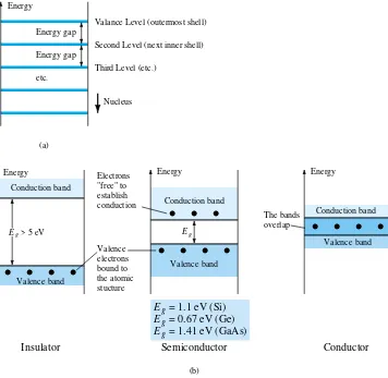
In the isolated atomic structure there are discrete (individual) energy levels associated with each orbiting electron, as shown in Fig. 1.8a. Each material will, in fact, have its own set of permissible energy levels for the electrons in its atomic structure.
The more distant the electron from the nucleus, the higher the energy state, and any electron that has left its parent atom has a higher energy state than any electron in the atomic structure.
Figure 1.8 Energy levels: (a)
discrete levels in isolated atomic structures; (b) conduction and valence bands of an insulator, semiconductor, and conductor.
Energy Energy Energy
E > 5 eVg
Valence band Conduction band
Valence band Conduction band
Conduction band The bands
overlap Electrons
"free" to establish conduction
Valence electrons bound to the atomic stucture
E g = 1.1 eV (Si) E g = 0.67 eV (Ge)
E g = 1.41 eV (GaAs)
Insulator Semiconductor
(b)
E Eg
Valence band
Conductor Energy gap
Energy gap etc.
Valance Level (outermost shell) Second Level (next inner shell) Third Level (etc.)
Energy
Nucleus
(a)
that ionization is the mechanism whereby an electron can absorb sufficient energy to break away from the atomic structure and enter the conduction band. You will note that the energy associated with each electron is measured in electron volts(eV). The
unit of measure is appropriate, since
WQV eV (1.2)
as derived from the defining equation for voltage VW/Q. The charge Qis the charge
associated with a single electron.
Substituting the charge of an electron and a potential difference of 1 volt into Eq. (1.2) will result in an energy level referred to as one electron volt. Since energy is
also measured in joules and the charge of one electron1.61019coulomb,
WQV(1.61019C)(1 V)
and 1 eV1.61019J (1.3)
At 0 K or absolute zero (273.15°C), all the valence electrons of semiconductor
materials find themselves locked in their outermost shell of the atom with energy levels associated with the valence band of Fig. 1.8b. However, at room temperature (300 K, 25°C) a large number of valence electrons have acquired sufficient energy to leave the valence band, cross the energy gap defined by Egin Fig. 1.8b and enter the
conduction band. For silicon Eg is 1.1 eV, for germanium 0.67 eV, and for gallium
arsenide 1.41 eV. The obviously lower Egfor germanium accounts for the increased
number of carriers in that material as compared to silicon at room temperature. Note for the insulator that the energy gap is typically 5 eV or more, which severely limits the number of electrons that can enter the conduction band at room temperature. The conductor has electrons in the conduction band even at 0 K. Quite obviously, there-fore, at room temperature there are more than enough free carriers to sustain a heavy flow of charge, or current.
We will find in Section 1.5 that if certain impurities are added to the intrinsic semiconductor materials, energy states in the forbidden bands will occur which will cause a net reduction in Egfor both semiconductor materials—consequently, increased
carrier density in the conduction band at room temperature!
1.5
EXTRINSIC MATERIALS—
n
- AND
p
-TYPE
The characteristics of semiconductor materials can be altered significantly by the ad-dition of certain impurity atoms into the relatively pure semiconductor material. These impurities, although only added to perhaps 1 part in 10 million, can alter the band structure sufficiently to totally change the electrical properties of the material.
A semiconductor material that has been subjected to the doping process is called an extrinsic material.
There are two extrinsic materials of immeasurable importance to semiconductor device fabrication: n-type and p-type. Each will be described in some detail in the
following paragraphs.
n
-Type Material
Both the n- and p-type materials are formed by adding a predetermined number of
impurity atoms into a germanium or silicon base. The n-type is created by
introduc-ing those impurity elements that have fivevalence electrons (pentavalent), such as an-timony, arsenic,and phosphorus.The effect of such impurity elements is indicated in
7
–
Antimony (Sb) impurity Si
–
– –
–
–
– –
–
–
– –
–
–
– –
–
–
– –
–
–
– –
–
–
– –
–
–
– –
–
–
– –
–
Si Si Si
Sb Si
Si Si
Si
Fifth valence electron of antimony
Figure 1.9 Antimony impurity
in n-type material.
Fig. 1.9 (using antimony as the impurity in a silicon base). Note that the four cova-lent bonds are still present. There is, however, an additional fifth electron due to the impurity atom, which is unassociated with any particular covalent bond. This
re-maining electron, loosely bound to its parent (antimony) atom, is relatively free to move within the newly formed n-type material. Since the inserted impurity atom has
donated a relatively “free” electron to the structure:
Diffused impurities with five valence electrons are called donor atoms.
It is important to realize that even though a large number of “free” carriers have been established in the n-type material, it is still electrically neutralsince ideally the
number of positively charged protons in the nuclei is still equal to the number of “free” and orbiting negatively charged electrons in the structure.
The effect of this doping process on the relative conductivity can best be described through the use of the energy-band diagram of Fig. 1.10. Note that a discrete energy level (called the donor level) appears in the forbidden band with an Eg significantly
less than that of the intrinsic material. Those “free” electrons due to the added im-purity sit at this energy level and have less difficulty absorbing a sufficient measure of thermal energy to move into the conduction band at room temperature. The result is that at room temperature, there are a large number of carriers (electrons) in the conduction level and the conductivity of the material increases significantly. At room temperature in an intrinsic Si material there is about one free electron for every 1012
atoms (1 to 109 for Ge). If our dosage level were 1 in 10 million (107), the ratio
(1012/107105) would indicate that the carrier concentration has increased by a
ra-tio of 100,000⬊1.
Figure 1.10 Effect of donor impurities on the energy band
structure.
Energy
Conduction band
Valence band
Donor energy level
g
E = 0.05 eV (Si), 0.01 eV (Ge) E as beforeg
p
-Type Material
The p-type material is formed by doping a pure germanium or silicon crystal with
impurity atoms having threevalence electrons. The elements most frequently used for
this purpose are boron, gallium, and indium. The effect of one of these elements,
boron, on a base of silicon is indicated in Fig. 1.11.
9
1.5 Extrinsic Materials—n- and p-Type
Figure 1.11 Boron impurity in
p-type material.
Note that there is now an insufficient number of electrons to complete the cova-lent bonds of the newly formed lattice. The resulting vacancy is called a holeand is
represented by a small circle or positive sign due to the absence of a negative charge. Since the resulting vacancy will readily accepta “free” electron:
The diffused impurities with three valence electrons are called acceptor atoms.
The resulting p-type material is electrically neutral, for the same reasons described
for the n-type material.
Electron versus Hole Flow
The effect of the hole on conduction is shown in Fig. 1.12. If a valence electron ac-quires sufficient kinetic energy to break its covalent bond and fills the void created by a hole, then a vacancy, or hole, will be created in the covalent bond that released the electron. There is, therefore, a transfer of holes to the left and electrons to the right, as shown in Fig. 1.12. The direction to be used in this text is that of conven-tional flow,which is indicated by the direction of hole flow.
Figure 1.12 Electron versus
Majority and Minority Carriers
In the intrinsic state, the number of free electrons in Ge or Si is due only to those few electrons in the valence band that have acquired sufficient energy from thermal or light sources to break the covalent bond or to the few impurities that could not be re-moved. The vacancies left behind in the covalent bonding structure represent our very limited supply of holes. In an n-type material, the number of holes has not changed
significantly from this intrinsic level. The net result, therefore, is that the number of electrons far outweighs the number of holes. For this reason:
In an n-type material (Fig. 1.13a) the electron is called the majority carrier and the hole the minority carrier.
For the p-type material the number of holes far outweighs the number of
elec-trons, as shown in Fig. 1.13b. Therefore:
In a p-type material the hole is the majority carrier and the electron is the minority carrier.
When the fifth electron of a donor atom leaves the parent atom, the atom remaining acquires a net positive charge: hence the positive sign in the donor-ion representation. For similar reasons, the negative sign appears in the acceptor ion.
The n- and p-type materials represent the basic building blocks of semiconductor
devices. We will find in the next section that the “joining” of a single n-type
mater-ial with a p-type material will result in a semiconductor element of considerable
im-portance in electronic systems.
Figure 1.13 (a) n-type material; (b) p-type material.
+
–
+
+
–
–
–
–
+
–
–
–
–
–
–
–
+
Minority carrier Minority carrier p-type n-type Donor ions Majority carriers Acceptor ions Majority carriers+
+
+
+
+
+
+
+
+
–
+
–
–
–
–
–
–
+
+
+
+
–
–
+
+
–
–
+
+
–
–
–
+
+
+
–
+
+
+
(a) (b)1.6
SEMICONDUCTOR DIODE
In Section 1.5 both the n- and p-type materials were introduced. The semiconductor
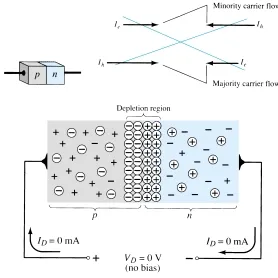
diode is formed by simply bringing these materials together (constructed from the same base—Ge or Si), as shown in Fig. 1.14, using techniques to be described in Chapter 20. At the instant the two materials are “joined” the electrons and holes in the region of the junction will combine, resulting in a lack of carriers in the region near the junction.
This region of uncovered positive and negative ions is called the depletion re-gion due to the depletion of carriers in this rere-gion.
Since the diode is a two-terminal device, the application of a voltage across its terminals leaves three possibilities:no bias(VD0 V),forward bias(VD 0 V), and reverse bias (VD0 V). Each is a condition that will result in a response that the
No Applied Bias (
V
D0 V)
Under no-bias (no applied voltage) conditions, any minority carriers (holes) in the
n-type material that find themselves within the depletion region will pass directly into
the p-type material. The closer the minority carrier is to the junction, the greater the
attraction for the layer of negative ions and the less the opposition of the positive ions in the depletion region of the n-type material. For the purposes of future discussions
we shall assume that all the minority carriers of the n-type material that find
them-selves in the depletion region due to their random motion will pass directly into the
p-type material. Similar discussion can be applied to the minority carriers (electrons)
of the p-type material. This carrier flow has been indicated in Fig. 1.14 for the
mi-nority carriers of each material.
The majority carriers (electrons) of the n-type material must overcome the
at-tractive forces of the layer of positive ions in the n-type material and the shield of
negative ions in the p-type material to migrate into the area beyond the depletion
re-gion of the p-type material. However, the number of majority carriers is so large in
the n-type material that there will invariably be a small number of majority carriers
with sufficient kinetic energy to pass through the depletion region into the p-type
ma-terial. Again, the same type of discussion can be applied to the majority carriers (holes) of the p-type material. The resulting flow due to the majority carriers is also shown
in Fig. 1.14.
A close examination of Fig. 1.14 will reveal that the relative magnitudes of the flow vectors are such that the net flow in either direction is zero. This cancellation of vectors has been indicated by crossed lines. The length of the vector representing hole flow has been drawn longer than that for electron flow to demonstrate that the mag-nitude of each need not be the same for cancellation and that the doping levels for each material may result in an unequal carrier flow of holes and electrons. In sum-mary, therefore:
In the absence of an applied bias voltage, the net flow of charge in any one direction for a semiconductor diode is zero.
11
1.6 Semiconductor Diode
Figure 1.14 p-njunction with
The symbol for a diode is repeated in Fig. 1.15 with the associated n- and p-type
regions. Note that the arrow is associated with the p-type component and the bar with
the n-type region. As indicated, for VD0 V, the current in any direction is 0 mA.
Reverse-Bias Condition (
V
D0 V)
If an external potential of Vvolts is applied across the p-njunction such that the
pos-itive terminal is connected to the n-type material and the negative terminal is
con-nected to the p-type material as shown in Fig. 1.16, the number of uncovered
posi-tive ions in the depletion region of the n-type material will increase due to the large
number of “free” electrons drawn to the positive potential of the applied voltage. For similar reasons, the number of uncovered negative ions will increase in the p-type
material. The net effect, therefore, is a widening of the depletion region. This widen-ing of the depletion region will establish too great a barrier for the majority carriers to overcome, effectively reducing the majority carrier flow to zero as shown in Fig. 1.16.
Figure 1.17 Reverse-bias
conditions for a semiconductor diode.
Figure 1.15 No-bias conditions
for a semiconductor diode.
The number of minority carriers, however, that find themselves entering the de-pletion region will not change, resulting in minority-carrier flow vectors of the same magnitude indicated in Fig. 1.14 with no applied voltage.
The current that exists under reverse-bias conditions is called the reverse sat-uration current and is represented by Is.
The reverse saturation current is seldom more than a few microamperes except for high-power devices. In fact, in recent years its level is typically in the nanoampere range for silicon devices and in the low-microampere range for germanium. The term
saturationcomes from the fact that it reaches its maximum level quickly and does not
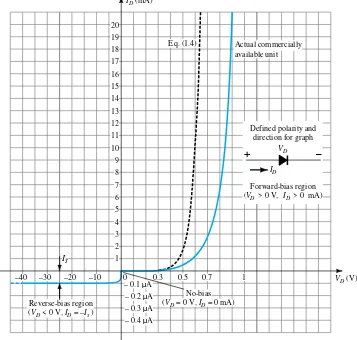
change significantly with increase in the reverse-bias potential, as shown on the diode characteristics of Fig. 1.19 for VD0 V. The reverse-biased conditions are depicted
in Fig. 1.17 for the diode symbol and p-njunction. Note, in particular, that the
direc-tion of Isis against the arrow of the symbol. Note also that the negative potential is
connected to the p-type material and thepositive potential to the n-type material—the
difference in underlined letters for each region revealing a reverse-bias condition.
Forward-Bias Condition (
V
D0 V)
A forward-biasor “on” condition is established by applying the positive potential to
the p-type material and the negative potential to the n-type material as shown in Fig.
1.18. For future reference, therefore:
A semiconductor diode is forward-biased when the association p-type and p os-itive and n-type and negative has been established.
Figure 1.16 Reverse-biased
13
The application of a forward-bias potential VD will “pressure” electrons in the n-type material and holes in the p-type material to recombine with the ions near the
boundary and reduce the width of the depletion region as shown in Fig. 1.18. The re-sulting minority-carrier flow of electrons from the p-type material to the n-type
ma-terial (and of holes from the n-type material to the p-type material) has not changed
in magnitude (since the conduction level is controlled primarily by the limited num-ber of impurities in the material), but the reduction in the width of the depletion re-gion has resulted in a heavy majority flow across the junction. An electron of the
n-type material now “sees” a reduced barrier at the junction due to the reduced
de-pletion region and a strong attraction for the positive potential applied to the p-type
material. As the applied bias increases in magnitude the depletion region will con-tinue to decrease in width until a flood of electrons can pass through the junction,
re-1.6 Semiconductor Diode
Figure 1.18 Forward-biased p-n
junction.
Figure 1.19 Silicon semiconductor
diode characteristics.
10 11 12 13 14 15 16 17 18 19 20
1 2 3 4 5 6 7 8 9
0.3 0.5 0.7 1 –10
–20 –30 –40
ID (mA)
(V) D
V
D
V
– +
Defined polarity and direction for graph
Forward-bias region (V > 0 V, I > 0 mA)
D
I
D
VD I
s I
– 0.2 uA – 0.3 uA – 0.4 uA
µ
0
No-bias (VD = 0 V, ID = 0 mA) – 0.1 uA
µ µ µ
Reverse-bias region (VD < 0 V, ID = –Is )
sulting in an exponential rise in current as shown in the forward-bias region of the characteristics of Fig. 1.19. Note that the vertical scale of Fig. 1.19 is measured in milliamperes (although some semiconductor diodes will have a vertical scale mea-sured in amperes) and the horizontal scale in the forward-bias region has a maximum of 1 V. Typically, therefore, the voltage across a forward-biased diode will be less than 1 V. Note also, how quickly the current rises beyond the knee of the curve.
It can be demonstrated through the use of solid-state physics that the general char-acteristics of a semiconductor diode can be defined by the following equation for the forward- and reverse-bias regions:
IDIs(e
kVD/TK1) (1.4)
where Isreverse saturation current
k11,600/ with 1 for Ge and 2 for Si for relatively low levels
of diode current (at or below the knee of the curve) and 1 for Ge
and Si for higher levels of diode current (in the rapidly increasing sec-tion of the curve)
TKTC273°
A plot of Eq. (1.4) is provided in Fig. 1.19. If we expand Eq. (1.4) into the fol-lowing form, the contributing component for each region of Fig. 1.19 can easily be described:
IDIse kVD/TK
Is
For positive values of VD the first term of the equation above will grow very
quickly and overpower the effect of the second term. The result is that for positive values of VD, IDwill be positive and grow as the function ye
x appearing in Fig.
1.20. At VD0 V, Eq. (1.4) becomes IDIs(e01)Is(11)0 mA as
ap-pearing in Fig. 1.19. For negative values of VDthe first term will quickly drop off
be-low Is, resulting in ID Is, which is simply the horizontal line of Fig. 1.19. The
break in the characteristics at VD0 V is simply due to the dramatic change in scale
from mA to A.
Note in Fig. 1.19 that the commercially available unit has characteristics that are shifted to the right by a few tenths of a volt. This is due to the internal “body” resis-tance and external “contact” resisresis-tance of a diode. Each contributes to an additional voltage at the same current level as determined by Ohm’s law (VIR). In time, as
production methods improve, this difference will decrease and the actual characteris-tics approach those of Eq. (1.4).
It is important to note the change in scale for the vertical and horizontal axes. For positive values of IDthe scale is in milliamperes and the current scale below the axis
is in microamperes (or possibly nanoamperes). For VDthe scale for positive values is
in tenths of volts and for negative values the scale is in tens of volts.
Initially, Eq. (1.4) does appear somewhat complex and may develop an unwar-ranted fear that it will be applied for all the diode applications to follow. Fortunately, however, a number of approximations will be made in a later section that will negate the need to apply Eq. (1.4) and provide a solution with a minimum of mathematical difficulty.
Before leaving the subject of the forward-bias state the conditions for conduction (the “on” state) are repeated in Fig. 1.21 with the required biasing polarities and the resulting direction of majority-carrier flow. Note in particular how the direction of conduction matches the arrow in the symbol (as revealed for the ideal diode).
Zener Region
Even though the scale of Fig. 1.19 is in tens of volts in the negative region, there is a point where the application of too negative a voltage will result in a sharp change
Figure 1.20 Plot of ex.
Figure 1.21 Forward-bias
15
1.6 Semiconductor Diode
Figure 1.22 Zener region.
in the characteristics, as shown in Fig. 1.22. The current increases at a very rapid rate in a direction opposite to that of the positive voltage region. The reverse-bias poten-tial that results in this dramatic change in characteristics is called the Zener potential
and is given the symbol VZ.
As the voltage across the diode increases in the reverse-bias region, the velocity of the minority carriers responsible for the reverse saturation current Iswill also
in-crease. Eventually, their velocity and associated kinetic energy (WK12mv2) will be
sufficient to release additional carriers through collisions with otherwise stable atomic structures. That is, an ionizationprocess will result whereby valence electrons absorb
sufficient energy to leave the parent atom. These additional carriers can then aid the ionization process to the point where a high avalanchecurrent is established and the avalanche breakdownregion determined.
The avalanche region (VZ) can be brought closer to the vertical axis by increasing
the doping levels in the p- and n-type materials. However, as VZdecreases to very low
levels, such as 5 V, another mechanism, called Zener breakdown,will contribute to
the sharp change in the characteristic. It occurs because there is a strong electric field in the region of the junction that can disrupt the bonding forces within the atom and “generate” carriers. Although the Zener breakdown mechanism is a significant contrib-utor only at lower levels of VZ, this sharp change in the characteristic at any level is
called the Zener region and diodes employing this unique portion of the characteristic
of a p-njunction are called Zener diodes.They are described in detail in Section 1.14.
The Zener region of the semiconductor diode described must be avoided if the re-sponse of a system is not to be completely altered by the sharp change in character-istics in this reverse-voltage region.
The maximum reverse-bias potential that can be applied before entering the Zener region is called the peak inverse voltage (referred to simply as the PIV rating)or the peak reverse voltage (denoted by PRV rating).
If an application requires a PIV rating greater than that of a single unit, a num-ber of diodes of the same characteristics can be connected in series. Diodes are also connected in parallel to increase the current-carrying capacity.
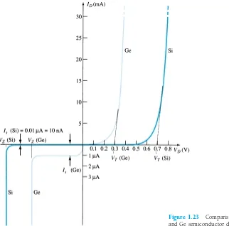
Silicon versus Germanium
forward-bias voltage required to reach the region of upward swing. It is typically of the order of magnitude of 0.7 V for commerciallyavailable silicon diodes and 0.3 V
for germanium diodes when rounded off to the nearest tenths. The increased offset for silicon is due primarily to the factor in Eq. (1.4). This factor plays a part in
de-termining the shape of the curve only at very low current levels. Once the curve starts its vertical rise, the factor drops to 1 (the continuous value for germanium). This is
evidenced by the similarities in the curves once the offset potential is reached. The potential at which this rise occurs is commonly referred to as the offset, threshold,or firing potential.Frequently, the first letter of a term that describes a particular
quan-tity is used in the notation for that quanquan-tity. However, to ensure a minimum of con-fusion with other terms, such as output voltage (Vo) and forward voltage (VF), the
no-tation VThas been adopted for this book, from the word “threshold.”
In review:
VT0.7 (Si) VT0.3 (Ge)
Obviously, the closer the upward swing is to the vertical axis, the more “ideal” the device. However, the other characteristics of silicon as compared to germanium still make it the choice in the majority of commercially available units.
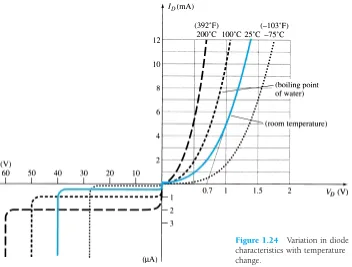
Temperature Effects
Temperature can have a marked effect on the characteristics of a silicon semicon-ductor diode as witnessed by a typical silicon diode in Fig. 1.24. It has been found experimentally that:
The reverse saturation current Iswill just about double in magnitude for every 10°C increase in temperature.
Figure 1.23 Comparison of Si
17
1.7 Resistance Levels
Figure 1.24 Variation in diode
characteristics with temperature change.
It is not uncommon for a germanium diode with an Isin the order of 1 or 2 A
at 25°C to have a leakage current of 100 A0.1 mA at a temperature of 100°C.
Current levels of this magnitude in the reverse-bias region would certainly question our desired open-circuit condition in the reverse-bias region. Typical values of Isfor
silicon are much lower than that of germanium for similar power and current levels as shown in Fig. 1.23. The result is that even at high temperatures the levels of Isfor
silicon diodes do not reach the same high levels obtained for germanium—a very im-portant reason that silicon devices enjoy a significantly higher level of development and utilization in design. Fundamentally, the open-circuit equivalent in the reverse-bias region is better realized at any temperature with silicon than with germanium. The increasing levels of Iswith temperature account for the lower levels of
thresh-old voltage, as shown in Fig. 1.24. Simply increase the level of Isin Eq. (1.4) and
note the earlier rise in diode current. Of course, the level of TKalso will be
increas-ing in the same equation, but the increasincreas-ing level of Iswill overpower the smaller
per-cent change in TK. As the temperature increases the forward characteristics are
actu-ally becoming more “ideal,” but we will find when we review the specifications sheets that temperatures beyond the normal operating range can have a very detrimental ef-fect on the diode’s maximum power and current levels. In the reverse-bias region the breakdown voltage is increasing with temperature, but note the undesirable increase in reverse saturation current.
1.7
RESISTANCE LEVELS
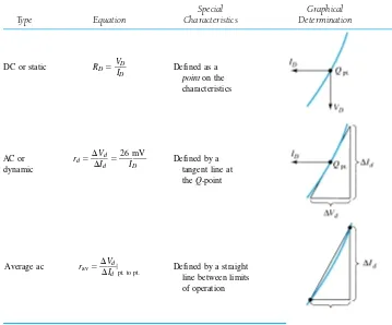
DC or Static Resistance
The application of a dc voltage to a circuit containing a semiconductor diode will re-sult in an operating point on the characteristic curve that will not change with time. The resistance of the diode at the operating point can be found simply by finding the corresponding levels of VDand IDas shown in Fig. 1.25 and applying the following
equation:
RD V
ID D
(1.5)
The dc resistance levels at the knee and below will be greater than the resistance levels obtained for the vertical rise section of the characteristics. The resistance lev-els in the reverse-bias region will naturally be quite high. Since ohmmeters typically employ a relatively constant-current source, the resistance determined will be at a pre-set current level (typically, a few milliamperes).
Figure 1.25 Determining the dc
resistance of a diode at a particu-lar operating point.
In general, therefore, the lower the current through a diode the higher the dc resistance level.
Determine the dc resistance levels for the diode of Fig. 1.26 at (a) ID2 mA
(b) ID20 mA
(c) VD 10 V
Solution
(a) At ID2 mA,VD0.5 V (from the curve) and
RD V
ID D
2 0.
m 5 V
A 250 ⍀
EXAMPLE 1.1
19
Figure 1.28 Determining the ac
resistance at a Q-point.
A straight line drawn tangent to the curve through the Q-point as shown in Fig.
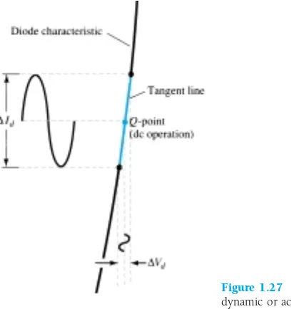
1.28 will define a particular change in voltage and current that can be used to deter-mine the acor dynamicresistance for this region of the diode characteristics. An
ef-fort should be made to keep the change in voltage and current as small as possible and equidistant to either side of the Q-point. In equation form,
rd
V
I d
d
where signifies a finite change in the quantity. (1.6)
The steeper the slope, the less the value of Vdfor the same change in Idand the
less the resistance. The ac resistance in the vertical-rise region of the characteristic is therefore quite small, while the ac resistance is much higher at low current levels.
In general, therefore, the lower the Q-point of operation (smaller current or lower voltage) the higher the ac resistance.
(b) At ID20 mA, VD0.8 V (from the curve) and
RD V
ID D
2 0
0 .8
m V
A 40 ⍀ (c) At VD 10 V,ID Is 1 A (from the curve) and
RD V
ID D
1 10
V
A 10 M⍀
clearly supporting some of the earlier comments regarding the dc resistance levels of a diode.
AC or Dynamic Resistance
It is obvious from Eq. 1.5 and Example 1.1 that the dc resistance of a diode is inde-pendent of the shape of the characteristic in the region surrounding the point of inter-est. If a sinusoidal rather than dc input is applied, the situation will change completely. The varying input will move the instantaneous operating point up and down a region of the characteristics and thus defines a specific change in current and voltage as shown in Fig. 1.27. With no applied varying signal, the point of operation would be the Q-point appearing on Fig. 1.27 determined by the applied dc levels. The
des-ignation Q-pointis derived from the word quiescent,which means “still or unvarying.”
Figure 1.27 Defining the
dynamic or ac resistance.
Solution
(a) For ID2 mA; the tangent line at ID2 mA was drawn as shown in the figure
and a swing of 2 mA above and below the specified diode current was chosen. At ID4 mA, VD0.76 V, and at ID0 mA, VD0.65 V. The resulting
changes in current and voltage are
Id4 mA0 mA4 mA
and Vd0.76 V0.65 V0.11 V
and the ac resistance:
rd
V Id
d
0
4 .1
m 1 A
V
27.5 ⍀
(b) For ID25 mA, the tangent line at ID25 mA was drawn as shown on the
fig-ure and a swing of 5 mA above and below the specified diode current was cho-sen. At ID30 mA,VD0.8 V, and at ID20 mA,VD0.78 V. The
result-ing changes in current and voltage are
Id30 mA20 mA10 mA
and Vd0.8 V0.78 V0.02 V
and the ac resistance is
rd
V Id
d
1 0 0
.0 m 2 V
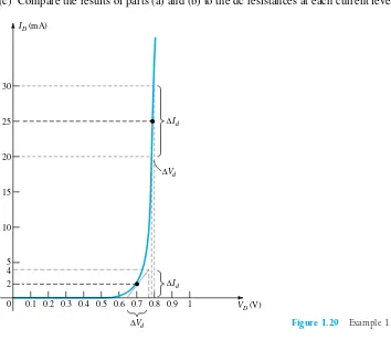
A 2 ⍀ For the characteristics of Fig. 1.29:
(a) Determine the ac resistance at ID2 mA.
(b) Determine the ac resistance at ID25 mA.
(c) Compare the results of parts (a) and (b) to the dc resistances at each current level.
EXAMPLE 1.2
Figure 1.29 Example 1.2
V (V)D I (mA)ID
0 5 10 15 20 25 30
2 4
0.1 0.2 0.3 0.4 0.5 0.6 0.7 0.8 0.9 1
∆Id
∆Id
∆Vd
21
1.7 Resistance Levels
(c) For ID2 mA,VD0.7 V and
RD V ID D 2 0. m 7 V
A 350 ⍀ which far exceeds the rdof 27.5 .
For ID25 mA,VD0.79 V and
RD V ID D 2 0 5 .7 m 9 V
A 31.62 ⍀
which far exceeds the rdof 2 .
We have found the dynamic resistance graphically, but there is a basic definition in differential calculus which states:
The derivative of a function at a point is equal to the slope of the tangent line drawn at that point.
Equation (1.6), as defined by Fig. 1.28, is, therefore, essentially finding the deriva-tive of the function at the Q-point of operation. If we find the derivative of the
gen-eral equation (1.4) for the semiconductor diode with respect to the applied forward bias and then invert the result, we will have an equation for the dynamic or ac resis-tance in that region. That is, taking the derivative of Eq. (1.4) with respect to the ap-plied bias will result in
dV d
D
(ID) d
d V[Is(e
kVD/TK1)]
and d d V ID D T k K
(IDIs)
following a few basic maneuvers of differential calculus. In general, IDIs in the
vertical slope section of the characteristics and
d d V ID D ⬵ T k K ID
Substituting 1 for Ge and Si in the vertical-rise section of the characteristics, we
obtain k 11, 600 11, 1 600 11,600
and at room temperature,
TKTC273°25°273°298°
so that T k K 11 2 , 9 6 8 00 ⬵38.93 and d d V ID D 38.93ID
Flipping the result to define a resistance ratio (RV/I) gives us
d
d V
ID D
⬵0.
I
0
D
26
or rd 26
ID
mV
Ge,Si
The significance of Eq. (1.7) must be clearly understood. It implies that the dynamic resistance can be found simply by substituting the quiescent value of the diode cur-rent into the equation. There is no need to have the characteristics available or to worry about sketching tangent lines as defined by Eq. (1.6). It is important to keep in mind, however, that Eq. (1.7) is accurate only for values of IDin the vertical-rise
section of the curve. For lesser values of ID,2 (silicon) and the value of rd
ob-tained must be multiplied by a factor of 2. For small values of IDbelow the knee of
the curve, Eq. (1.7) becomes inappropriate.
All the resistance levels determined thus far have been defined by the p-n
junc-tion and do not include the resistance of the semiconductor material itself (called body
resistance) and the resistance introduced by the connection between the semiconduc-tor material and the external metallic conducsemiconduc-tor (called contactresistance). These
ad-ditional resistance levels can be included in Eq. (1.7) by adding resistance denoted by rBas appearing in Eq. (1.8). The resistance rd, therefore, includes the dynamic
re-sistance defined by Eq. 1.7 and the rere-sistance rBjust introduced.
rd
26
ID
mV
rB ohms (1.8)
The factor rBcan range from typically 0.1 for high-power devices to 2 for
some low-power, general-purpose diodes. For Example 1.2 the ac resistance at 25 mA was calculated to be 2 . Using Eq. (1.7), we have
rd 26 ID
mV
2 2 5 6
m mV
A 1.04 ⍀
The difference of about 1 could be treated as the contribution of rB.
For Example 1.2 the ac resistance at 2 mA was calculated to be 27.5 . Using
Eq. (1.7) but multiplying by a factor of 2 for this region (in the knee of the curve
2),
rd2
冢
26
ID
mV
冣
2冢
22 6
m m
A V
冣
2(13 )26 ⍀The difference of 1.5 could be treated as the contribution due to rB.
In reality, determining rdto a high degree of accuracy from a characteristic curve
using Eq. (1.6) is a difficult process at best and the results have to be treated with a grain of salt. At low levels of diode current the factor rB is normally small enough
compared to rdto permit ignoring its impact on the ac diode resistance. At high
lev-els of current the level of rBmay approach that of rd, but since there will frequently
be other resistive elements of a much larger magnitude in series with the diode we will assume in this book that the ac resistance is determined solely by rdand the
im-pact of rBwill be ignored unless otherwise noted. Technological improvements of
re-cent years suggest that the level of rB will continue to decrease in magnitude and
eventually become a factor that can certainly be ignored in comparison to rd.
The discussion above has centered solely on the forward-bias region. In