Power MOSFET
IRFZ44, SiHFZ44
Vishay Siliconix
FEATURES
• Dynamic dV/dt Rating
• 175 °C Operating Temperature
• Fast Switching
• Ease of Paralleling
• Simple Drive Requirements
• Compliant to RoHS Directive 2002/95/EC
DESCRIPTION
Third generation Power MOSFETs from Vishay provide the
designer with the best combination of fast switching,
ruggedized device design, low on-resistance and
cost-effectiveness.
The TO-220AB package is universially preferred for
commercial-industrial applications at power dissipation
levels to approximately 50 W. The low thermal resistance
and low package cost of the TO-220AB contribute to its
wide acceptance throughout the industry.
Notes
a. Repetitive rating; pulse width limited by maximum junction temperature (see fig. 11). b. VDD = 25 V, starting TJ = 25 °C, L = 44 μH, Rg = 25 Ω, IAS = 51 A (see fig. 12).
N-Channel MOSFET G
Lead (Pb)-free IRFZ44PbF
SiHFZ44-E3
SnPb IRFZ44
SiHFZ44
ABSOLUTE MAXIMUM RATINGS
(T
C= 25 °C, unless otherwise noted)
PARAMETER SYMBOL LIMIT UNIT
Drain-Source Voltage VDS 60
V
Gate-Source Voltage VGS ± 20
Continuous Drain Currente
VGS at 10 V
Pulsed Drain Currenta I
DM 200
Linear Derating Factor 1.0 W/°C
Single Pulse Avalanche Energyb E
AS 100 mJ
Maximum Power Dissipation TC = 25 °C PD 150 W
Peak Diode Recovery dV/dtc dV/dt 4.5 V/ns
Operating Junction and Storage Temperature Range TJ, Tstg - 55 to + 175
°C
Soldering Recommendations (Peak Temperature)d for 10 s 300
Mounting Torque 6-32 or M3 screw 10 lbf · in
IRFZ44, SiHFZ44
Vishay Siliconix
Notes
a. Repetitive rating; pulse width limited by maximum junction temperature (see fig. 11). b. Pulse width ≤ 300 μs; duty cycle ≤ 2 %.
THERMAL RESISTANCE RATINGS
PARAMETER SYMBOL TYP. MAX. UNIT
Maximum Junction-to-Ambient RthJA - 62
°C/W
Case-to-Sink, Flat, Greased Surface RthCS 0.50
-Maximum Junction-to-Case (Drain) RthJC - 1.0
SPECIFICATIONS
(T
J= 25 °C, unless otherwise noted)
PARAMETER SYMBOL TEST CONDITIONS MIN. TYP. MAX. UNIT
Static
Drain-Source Breakdown Voltage VDS VGS = 0 V, ID = 250 μA 60 - - V
VDS Temperature Coefficient ΔVDS/TJ Reference to 25 °C, ID = 1 mA - 0.060 - V/°C Gate-Source Threshold Voltage VGS(th) VDS = VGS, ID = 250 μA 2.0 - 4.0 V
Gate-Source Leakage IGSS VGS = ± 20 V - - ± 100 nA
Zero Gate Voltage Drain Current IDSS
VDS = 60 V, VGS = 0 V - - 25
Input Capacitance Ciss V
GS = 0 V,
Reverse Transfer Capacitance Crss - 170
-Total Gate Charge Qg
Turn-On Delay Time td(on)
VDD = 30 V, ID = 51 A,
Internal Drain Inductance LD Between lead, 6 mm (0.25") from package and center of die contact
- 4.5
-nH
Internal Source Inductance LS - 7.5
-Drain-Source Body Diode Characteristics
Continuous Source-Drain Diode Current IS MOSFET symbol showing the integral reverse p - n junction diode
- - 50
A Pulsed Diode Forward Currenta I
SM - - 200
Body Diode Voltage VSD TJ = 25 °C, IS = 51 A, VGS = 0 Vb - - 2.5 V
Body Diode Reverse Recovery Time trr
TJ = 25 °C, IF = 51 A, dI/dt = 100 A/µs
- 120 180 ns
Body Diode Reverse Recovery Charge Qrr - 0.53 0.80 nC
IRFZ44, SiHFZ44
Vishay Siliconix
TYPICAL CHARACTERISTICS
(25 °C, unless otherwise noted)
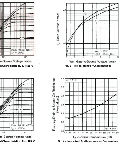
Fig. 1 Typical Output Characteristics, TC = 25 °C
Fig. 2 - Typical Output Characteristics, TC = 175 °C
Fig. 3 - Typical Transfer Characteristics
IRFZ44, SiHFZ44
Vishay Siliconix
Fig. 5 - Typical Capacitance vs. Drain-to-Source Voltage
Fig. 6 - Typical Gate Charge vs. Gate-to-Source Voltage
Fig. 7 - Typical Source-Drain Diode Forward Voltage
IRFZ44, SiHFZ44
Vishay Siliconix
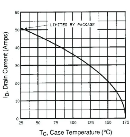
Fig. 9 - Maximum Drain Current vs. Case Temperature
Fig. 10a - Switching Time Test Circuit
Fig. 10b - Switching Time Waveforms
Fig. 11 - Maximum Effective Transient Thermal Impedance, Junction-to-Case
Pulse width ≤ 1 µs required IAS
IAS VDS
VDD VDS
IRFZ44, SiHFZ44
Vishay Siliconix
Fig. 12c - Maximum Avalanche Energy vs. Drain Current
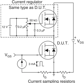
Fig. 13a - Basic Gate Charge Waveform Fig. 13b - Gate Charge Test QGS QGD
QG
VG
Charge 10 V
D.U.T.
3 mA VGS
VDS
IG ID 0.3 µF
0.2 µF 50 kΩ 12 V
Current regulator
Current sampling resistors Same type as D.U.T.
-IRFZ44, SiHFZ44
Vishay Siliconix
Fig. 14 - For N-Channel P.W. Period
dI/dt
Diode recovery dV/dt
Ripple≤ 5 %
Body diode forward drop Re-applied
voltage Reverse recovery current
Body diode forward current
VGS= 10 V a
ISD
Driver gate drive
D.U.T. lSD waveform
D.U.T. Circuit layout considerations
• Low stray inductance • Ground plane • Low leakage inductance
current transformer
Rg
Note
a. VGS = 5 V for logic level devices
Package Information
www.vishay.com
Vishay Siliconix
TO-220-1
Note
• M* = 0.052 inches to 0.064 inches (dimension including protrusion), heatsink hole for HVM
M*
DIM. MILLIMETERS INCHES
MIN. MAX. MIN. MAX.
A 4.24 4.65 0.167 0.183
b 0.69 1.02 0.027 0.040
b(1) 1.14 1.78 0.045 0.070
c 0.36 0.61 0.014 0.024
D 14.33 15.85 0.564 0.624
E 9.96 10.52 0.392 0.414
e 2.41 2.67 0.095 0.105
e(1) 4.88 5.28 0.192 0.208
F 1.14 1.40 0.045 0.055
H(1) 6.10 6.71 0.240 0.264
J(1) 2.41 2.92 0.095 0.115
L 13.36 14.40 0.526 0.567
L(1) 3.33 4.04 0.131 0.159
Ø P 3.53 3.94 0.139 0.155
Q 2.54 3.00 0.100 0.118
ECN: X15-0364-Rev. C, 14-Dec-15 DWG: 6031