CHARACTERIZATION OF NANO-STRUCTURES IN MATERIALS
BY TRANSMISSION ELECTRON MICROSCOPY
Y. Tomokiyo
Research Laboratory for High Voltage Electron Microscopy, Kyushu University Fukuoka 812-8581, Japan email:[email protected]
ABSTRACT
We will introduce the usefulness of convergent beam electron diffraction (CBED) in nano-characterization of materials: (1) Determination of local lattice strain in Si, (2) Determination of polarity of GaN of wurtzite structure , (3) Measurement of local oxygen concentration of the high Tc superconductor YBa2Cu3Oy.
Keywords: convergent beam electron diffraction
Makalah diterima 7 Juli 2007
1. INTRODUCTION
It has been very important with the development of the nanotechnology and materials to characterize the structures and the distribution of solute elements or impurities in an atomic or molecular scale and to analyze the atom bonding state. A transmission electron microscope (TEM) is one of the indispensable tools for the nano-analysis of materials. A recent TEM with a condenser-objective lens enables us to illuminate a convergent beam or a parallel beam depending on one’s research purpose (Tomokiyo , 1992; Tomokiyo, and Matsumura, 1998). Furthermore an imaging filter attached to a TEM can subtract the background originated from inelastically scattered electrons in diffraction patterns (Okuyama , et.al., 2002). As to a recording media , a slow-scan CCD camera or an imaging plate is usable. Both recording media store data as digital signals and hence have good interface with a computer. Furthermore both have the good linearity between input and output signals and have a wide dynamic range compared with a film with emulsion. We can therefore directly compare intensities of diffraction with those of
calculation to extract quantitative information on crystal structure (Tomokiyo , 1992; Tomokiyo, and Matsumura, 1998). The purpose of the present paper is to demonstrate the usefulness of CBED for nano-characterization.
2. CONVERGENT BEAM ELECTRON DIFFRACTION
A series of electron diffraction patterns taken from Si with different convergence angles is shown in Figure 1.
A radius of disc increases with the increase in convergence angle 2α. Broad fringes and dark straight line appear inside of central disc. The fringe contrast originates from the dynamical effect among diffraction of a 0-th order Laue zone, whereas dark line contrast results from the,
the geometry of a HOLZ pattern and comparing with a computer-simulated pattern. An example of the determination of a local lattice parameter is shown in Figure 3. It is possible to determine a lattice parameter of area smaller than several nm with the accuracy of 0.1% or better by adopting a technique mentioned above (Okuyama , et.al., 2002).
(2) We can know the crystal symmetry by observing the geometry of a HOLZ pattern (Okuyama , et.al., 2002). For instance the arrangement of diffraction spots in Figure 1(a) is hexagonal implying the six fold symmetry. We can, however, clearly observe a triangle formed with HOLZ lines in the center of the disc in Figure 1(d).
Figure 1. Diffraction patterns with different convergence angle 2α. Si: [111] incidence.
(a) 2α=2.7 mrad, (b) 2α=7.4mrad, (c) 2α=12 mrad, (d) Enlargement of the central disc of (c)
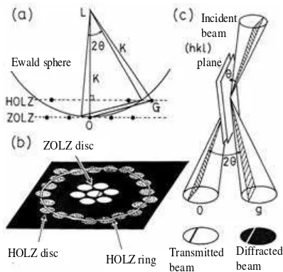
Figure 2. Principle of CBED.
(a) Cross section of reciprocal lattice plane and Ewald sphere, (b) Schematic drawing of zone axis pattern, (c) Origin of bright and dark line. parameter. kinematical diffraction from a higher order Laue zone (HOLZ) as schematically drawn in Figure 2. The degree of deviation from Bragg condition is different from point to point in a disc and hence, the fringes correspond to the rocking curve: diffraction intensity as a function of deviation A dark line appears as a pair with a parallel bright line like Kikuchi lines.
Figure 3. Determination of local lattice parameter by comparison with computer-simulation
HOLZ disc
HOLZ ring
Ewald sphere plane
Incident beam
Transmitted beam
Diffracted beam ZOLZ disc
HOLZ disc
HOLZ ring
Ewald sphere plane
Incident beam
Transmitted beam
Diffracted beam ZOLZ disc
(c)
(c) (d)(d)
(a) (b)
This result shows that Si has a three-fold symmetry along a [111] zone axis.
Usually the intensity of g and –g
diffraction is the same (Friedel’s law). As a result of dynamical diffraction effect among some diffraction, the contrast of discs is different between g and –g discs when the crystal has no center of symmetry. The polarity of zinc-blend or wurtzite structure that has no center of symmetry is known, by observing the change of contrast between CBED discs of g
and –g.
(3) When the convergence angle 2α is sufficiently large, plural discs may overlap, or plural diffractions may satisfy the Bragg condition. Since an illumination area is a few nm in radius, difference in crystal thickness is negligible within the area. When an incident beam is tilted so that systematic diffractions 0,
g, 2g, 3g, -, -, -, ng are excited, these diffractions satisfy the Bragg condition. Values of structure factors can be determined by analyzing plural diffractions appearing in a large angle CBED pattern(Akase, et. al., 2000). In the next section applications of above three items will be shown.
3. LOCAL LATTICE STRAIN NEAR A PLATELET OXIDE PRECI PITATE IN Si WAFER
Small residual stress in Si devices has become one of the serious problems in relation to the efficiency of good production and reliability of products with the proceeding of down-sizing of devices in semiconductor industry.
Figure 4. CBED-HOLZ patterns observed along [0 1 5 ] zone axis at different points from a precipitate in Si wafer. At 200 kV and at 100 K
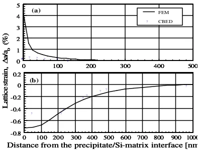
Thus the evaluation of distribution of residual stress is important. When local lattice strains are measured from HOLZ patterns of CBED, the distribution of residual stress is easily obtained through the continuum elasticity theory and the FEM, or the finite element method (Okuyama, et.al., 2002). We applied this method to the analysis of residual stress around a platelet oxide precipitate (2 --- 3 nm in thickness, 0.5 --- 1.0 µm in side length) which are formed in Si wafer as gettering sinks for impurities. Figure 4 shows CVED-HOLZ patterns observed near a precipitate.
HOLZ pattern close to the precipitate is diffuse and some of lines are split because of steep strain gradient and local lattice rotation. Lattice strains measured are plotted as a function of distance from a surface of oxide precipitate in Figure 5. It appears from Figure5 the lattice strain is tensile along a direction parallel to the surface of plate, while it is compressive along a perpendicular direction. The stress is almost released at the position about 1 µm from the plate. The continuous lines in Figure 5 indicate the curve reproduced by the FEM (Okuyama, et.al., 2002). The two dimensional distribution of residual stress around the precipitate is shown inFigure 6.
Distance from the precipitate/Si-matrix interface [nm]
Lattice strain,
∆
Distance from the precipitate/Si-matrix interface [nm]
Lattice strain,
∆
Distance from the precipitate/Si-matrix interface [nm]
Lattice strain,
∆
Figure 6. Stress field around a oxide precipitate in Si wafer
4. POLARITY OF GaN THIN FILM
HETEROEPITAXIALLY GROWN ON A GaAs SUBSTRATE
III-V or II-VI semiconductor crystals have been used as optoelectronics materials, light emitting diode, laser diode and etc. The crystals are wurtzite structure or zinc-blend structure that has the polarity. They are grown hetero- or home-epitaxially on a substrate crystal to form a thin film of single layer or multi-layers in order to control carrier mobility, band-gap, type of inter-band transition.
The growth mechanism and the surface structure depend on the polarity. The inversion of polarity brings anti-phase boundary, inversion domain boundary and lattice distortion. The determination and control of the polarity in III-V or II-VI semiconductors are important.
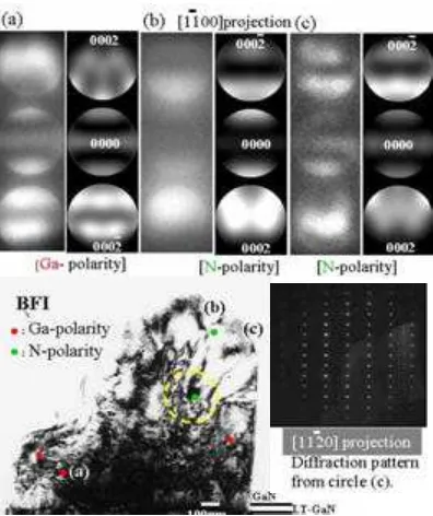
We tried to determine the polarity of GaN grown with HVPE (halide vapor phase epitaxy ) method on a GaAs (-1-1-1) ; As polarity substrate. Figure 7 shows CBED patterns observed and computer-simulated to decide the polarity and a bright field TEM image where points of CBED observation are indicated (Mitate, 2003). The polarity is easily known from the change of contrast between
g=0002 and –g=000-2. It is apparent from Figure7 that GaN layer has Ga-polarity from the early stage of the growth although GaAs substrate has As-polarity. N-polarity has also
partly observed in the GaN layer. Thus we can determine the polarity of local area with the spatial resolution of several nm in diameter.
5. LOCAL CHANGE IN OXYGEN
CONCENTRATION IN YBA2CU3OY
Oxygen is easily desorbed or absorbed on the surfaces of YBCO but is dependant on atmospheric parameters such as temperature and oxygen partial pressure. The value of oxygen concentration y in YBCO varies between 6 and 7. The critical temperature Tc
and the critical current density Jc of YBCO
depend on oxygen concentration of y.
Figure7. Polarity of GaN grown on a GaAs substrate of As polarity
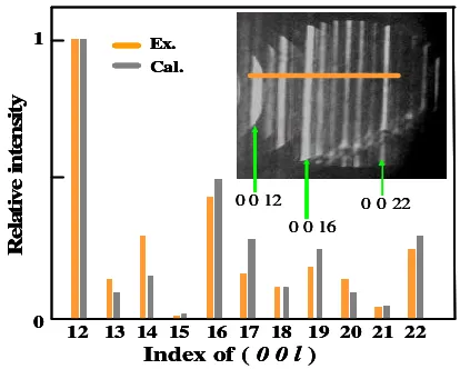
We tried to detect the local change in oxygen concentration with the CBED method. Our preliminary calculation predicts that intensity of 00l diffraction is sensitive to the change in y compared with other h00 or hk0 diffraction (Akase, et.al., 2000).
Oxygen concentration is determined with a comparison between the observed and calculated intensities of 00l reflections for 12 =
l = 22. An observed large angle CBED pattern and the intensity profile are shown in Figure8 where the convergence semi-angle α is 10 mrad. And the energy-filter is used to subtract the intensity, and specimen is cooled by liquid nitrogen stage to suppress the thermal vibration of atoms. Values of y, thus measured are indicated in Figure9 along with an bright-field TEM image. It is apparent from Figure9 that oxygen concentration y changes from point to point within a twin lamella (Tomokiyo, et.al., 2004). This local change in y is an origin of the peak effect in the Jc-H curve, the critical current
density Jc plotted as a function of applied
magnetic field H.
Figure 8. Large angle CBED pattern and comparison of intensities between observed and calculated 00l reflections of YBa2Cu3Oy
Figure 9. TEM bright-field image and values of oxygen concentration y in YBa2Cu3Oy, measured from CBED
6. CONCLUSION
Examples of the application of CBED were shown to demonstrate the usefulness for nano-characterization of crystalline materials. In conclusion it should be emphasized that the CBED methods provides us with local and quantitative information on crystal in contrast to the conventional selected area diffraction.
Furthermore CBED pattern is obtained from any area of the enlarged image under observation and this gives one to one correspondence between the diffraction and the nano-structure or morphology.
REFERENCES
Akase, Z, Y. Tomokiyo, Y. Tanaka and M. Watanabe, 2000. PhysicaC 339, 1-9. Mitate, T., 2003. Transmission Electron
Microscopy for Determination of Polarity in III-V Semiconductor Crystals, (PhD thesis), Faculty of Engineering Science, Kyushu University.
Okuyama, T., M. Nakayama, Y. Tomokiyo, and O.V. der Biest, 2002. J. Microscopy and Microanalysis, 8, 1-5.
41, 403-413.
Tomokiyo , Y., and S. Matsumura, 1998.
Materials Trans. JIM, Vol. 39, No .9, 927-937.