Novel InSb-based Quantum Well Transistors for
Ultra-High Speed, Low Power Logic Applications
T. Ashley, A. R. Barnes, L. Buckle, S. Datta*, A. B. Dean, M. T. Emeny, M. Fearn, D. G. Hayes, K. P. Hilton, R. Jefferies, T. Martin, K. J. Nash, T. J. Phillips, W. H. A. Tang, P. J. Wilding and R. Chau*
QinetiQ, Malvern Technology Center, St. Andrews Road, Malvern, WR14 3PS, UK
*Intel Corporation, Components Research, Logic Technology Development, Hillsboro, OR 97124, USA Email: [email protected]
Abstract
InSb-based quantum well field-effect transistors with gate length down to 0.2 µm are fabricated for the first time. Hall measurements show that room temperature electron mobilities over 30,000 cm2V-1s-1 are achieved with a sheet carrier density over 1×1012 cm- 2 in a modulation doped InSb quantum well with AlxIn1-xSb barrier layers. Devices with 0.2 µm gate length and 20% Al barrier exhibit DC transconductance of 625 µS/µm and fT of 150 GHz at VD S =0.5V. 0.2 µm devices fabricated on 30% Al barrier material show DC transconductance of 920 µS/µm at VD S =0.5V. Benchmarking against state-of-the-art Si MOSFET’s indicates that InSb QW transistors can achieve equivalent high speed performance with 5-10 times lower dynamic power dissipation and therefore are a promising device technology to complement scaled silicon-based devices for very low power, ultra-high speed logic applications.
1. Introduction
Indium antimonide (InSb) shows great promise as an ultra-fast, very low power digital logic technology as it has t he highest electron mobility and saturation velocity of any known semiconductor (Table 1). This performance can be accessed at room temperature using ExtractiveTM (minority carrier exclusion and extraction) technology, which mitigates the effect of the narrow band-gap on device leakage and breakdown. This was earlier demonstrated in a MISFET device, using an InSb device layer on an InSb substrate with a deposited SiO2 gate oxide [1]. In this paper, we report on the materials growth, device fabrication and c haracterization of an InSb channel quantum well FET, which uses a semi-insulating GaAs substrate, a relaxed metamorphic buffer layer of
AlyIn1-ySb to accommodate lattice mismatch, a
compressively strained InSb quantum well confined between layers of AlxIn1-xSb and a Schottky barrier metal gate. Careful materials structure design employing a modulation doping scheme achieves 295K electron mobility of over 30,000 cm2V- 1s-1 with a carrier density of over 1×1012 cm-2. Devices with gate length of 0.2 µm are fabricated and characterized, which demonstrate an fT of
150 GHz at VDS = 0.5V. Benchmarking with
state-of-the-art Si-based NMOS devices indicate that
InSb-based transistors achieve equivalent high speed performance with 5-10 times lower DC power dissipation, with potential for further increasing the performance when scaled to state-of-the-art Si device gate lengths.
Table 1. Channel Material Properties at 295K
Si GaAs In. 5 3Ga.47As InAs InSb
Electron Mobility
(cm2V- 1s- 1
ns=1x101 2/cm2)
600 4,600 7,800 20,000 30,000
Electron Saturation
Velocity (107 cm/s) 1.0 1.2 0.8 3.5 5.0
Ballistic Mean Free
Path (nm) 28 80 106 194 226
Energy Band-gap 1.12 1.42 0.72 0.36 0.18
2. Materials Growth and Results
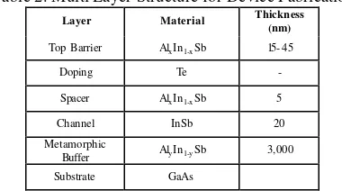
The InSb quantum well material was grown by solid-source molecular beam epitaxy (MBE) on a semi-insulating GaAs substrate. The layers from bottom to top consist of an accommodation layer, a 3 µm AlyIn1-ySb buffer, a 20 nm thick InSb quantum well, a 5nm thick AlxIn1- xSb spacer, a Te δ-doped donor sheet (~1×101 2 cm-2) and a 15-45 nm thick AlxIn1-xSb barrier layer (Table 2). Hall measurement of mobilities was performed at room temperature. Structures with the quantum well doped directly n-type with Te impurities gave carrier densities (ns) in the range of 0.8-1.2×1012 cm- 2 and mobilities in the range of 14,000-18,000 cm2V-1s-1. These were improved over earlier layers grown on 1 µm metamorphic buffer layers due to better material quality. We have also implemented a modulation doping scheme, with a Te δ-doped donor layer introduced in the
Table 2. Multi-Layer Structure for Device Fabrication
Layer Material Thickness
(nm)
Top Barrier AlxI n1-xSb 15- 4 5
Doping Te -
Spacer AlxI n1-xSb 5
Channel InSb 20
Metamorphic
Buffer AlyI n1-ySb 3,000
0 10000 20000 30000 40000
0 5E+11 1E+12 1.5E+12 2E+12
Sheet carrier density (cm-2)
Carrier mobility (cm
2 V -1 s -1 )
Doped Channel on 1 µm AlInSb
Doped Channel on 3 µm AlInSb
Remote doped on 3 µm AlInSb
Figure 1. Hall Mobility data on directly doped and modulation doped 20nm thick InSb quantum wells with 15% Al in the AlxIn1-xSb barrier layer.
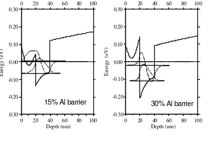
barrier layer above the quantum well, separated by a spacer layer. Single field Hall mobility measurements versus sheet carrier densities (ns) are shown in Figure 1. Modulation doped structures achieve a very high electron mobility of 30,000 cm2V- 1s-1 with ns = 5×1011 cm-2, but drops to around the same mobility ~16,000 cm2V-1s-1 as the directly doped structures for ns = 1×1012 cm- 2. It is believed that, in this regime, the mobility is not limited by ionized impurity scattering, despite the drop in mobility versus carrier density, since both the modulation -doped and the direct-doped structures show very similar mobility at high carrier densities, and both are below the expected value from an equivalent bulk-doped layer. Self-consistent Schrödinger-Poisson modeling of carrier distributions show that at higher carrier densities more
0 20 40 60 80 100
-0.30 -0.20 -0.10 0.00 0.10 0.20 0.30
0 20 40 60 80 100
Depth (nm)
Energy (eV)
0 20 40 60 80 100
-0.30 -0.20 -0.10 0.00 0.10 0.20 0.30
0 20 40 60 80 100
Depth (nm)
Energy (eV)
15% Al barrier 30% Al barrier
0 20 40 60 80 100
-0.30 -0.20 -0.10 0.00 0.10 0.20 0.30
0 20 40 60 80 100
Depth (nm)
Energy (eV)
0 20 40 60 80 100
-0.30 -0.20 -0.10 0.00 0.10 0.20 0.30
0 20 40 60 80 100
Depth (nm)
Energy (eV)
15% Al barrier 30% Al barrier
Figure 2. Calculated band structure and Schrödinger-Poisson solution of spatial redistribution of confined carrier population in various sub-bands in the quantum well for 15% and 30% Al percentage barriers.
carriers start to populate higher energy sub-bands that spread into the barriers, with consequent lower mobility, as shown in Figure 2. This modeling also predicts that using higher conduction band offset barriers would give increased mobility. We have grown layers with increased Al percentage in the barriers that show, for a given carrier density, the quantum well mobility increases monotonically with increasing Al percentage from 15% to 30%. Hall mobility measurements show that, with 30% Al in the barrier layers, the quantum well mobility achieved is over 30,000 cm2V-1s-1 at ns = 1.3×1012 cm-2, which is above the bulk InSb mobility versus doping concentration trend-line (Figure 3).
0 10000 20000 30000 40000
0 5E+11 1E+12 1.5E+12 2E+12
Sheet carrier density / cm-2
Carrier mobility /cm
2 V -1 s
-1
Remote doped in 15% barriers Remote doped in 20% barriers Remote doped in 30% barriers Bulk InSb (20nm well)
Figure 3. Hall Mobility data on modulation doped 20nm thick InSb quantum wells with 15%, 20% and 30% Al in the AlxIn1-xSb barrier layer.
3. Transistor Fabrication
Gate
Figure 4. SEM micrograph of a two-finger InSb quantum well transistor with gate air-bridge at the mesa edge. LG = 0.2 µm, LDS = 2.0 µ m.
4. DC Characterization
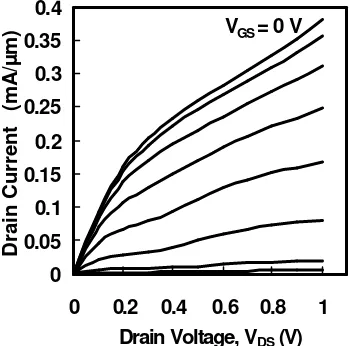
The InSb quantum well transistors were fabricated with gate lengths in the range 0.2-0.4 µm. A typical room temperature output characteristic of a 0.2 µm transistor fabricated on Type A material with a 50 nm 20% Al barrier is shown in Figure 5. The device exhibits good saturation characteristics with a knee voltage of 0.2 V and an off-state breakdown voltage of over 1.2 V. The low field source-drain resistance of this device is 1.2 Ω-mm, with source-drain separation of 2 µm and an ohmic contact resistance of 0.24 Ω-mm.
0
Gate Voltage, VGS (V)
Drain and Gate Current
(mA/µ
Gate Voltage, VGS (V)
Drain and Gate Current
(mA/µ
Gate Voltage, VGS (V)
Drain and Gate Current
(mA/µ
Gate Voltage, VGS (V)
Drain and Gate Current
(mA/µ
Figure 6. 0.2 µm LG InSb QW transistor transfer
characteristics at 295 K, Type A material, LDS = 2 µm, WG = 80 µm, VDS = 0.5 V, 50 mV.
Figure 6 shows the transfer characteristics of the device at VD S = 0.5 V and 50 mV. The peak gm for this device is 625 µS/µm at VDS = 0.5 V. The device shows an on-current of 263 µA/µm, off-current of 3.4 µA/µm, and a sub-threshold slope of 142 mV/decade at VDS = 0.5 V. The off-state current is limited by gate (non-optimized) to drain leakage as indicated in Figure 6. Using higher Al percentage barriers allows the barrier to be thinned, improving gm and subthreshold slope. Figure 7 shows the preliminary DC results of a 0.2 µm InSb quantum well transistor fabricated with Type B material with a 20 nm 30% Al barrier layer and mobility of 32,000 cm2V-1s-1 at
Drain and Gate Current (
mA
Drain and Gate Current (
mA
Figure 7. 0.2 µm LG InSb QW transistor transfer
5. High Frequency Characterization
RF characteristics of the Type A InSb transistors were obtained at room temperature through on -wafer S-parameter measurements at frequencies up to 50 GHz by using an HP 8510C vector network analyzer. Figure 9 shows the frequency depen dence of the short circuit current gain |h21|, MAG/MSG and Mason’s unilateral power gain Ug for the 0.2 µm gate length InSb transistor at VD S = 0.5 V and VGS = -0.4 V. The parasitic capacitances associated with the probe pads were subtracted from the measured S-parameters through a two-step de-embedding process. We obtain an fT of 150 GHz by ext rapolating |h21|2 with a slope of –20 dB/decade using a least squares fit. The maximum oscillation frequency fmax is around 190 GHz from both MSG/MAG and Ug, yielding an fmax/fT ratio of 1.3. Figure 10 compares the high frequency (fT)
0 10 20 30 40
0.1 1 1 0 100 1000
Frequency (GHz)
Gain (dB)
h21 MSG/MAG Ug VDS = 0.5V, VGS = -0.4V
fT= 150GHz
fmax~ 190GHz
0 10 20 30 40
0.1 1 1 0 100 1000
Frequency (GHz)
Gain (dB)
h21 MSG/MAG Ug VDS = 0.5V, VGS = -0.4V
fT= 150GHz
fmax~ 190GHz
fT= 150GHz
fmax~ 190GHz
Figure 9. Intrinsic current gain |h21|, MSG/MAG and Mason’s gain Ug (after de-embedding) versus frequency for 0.2 µm InSb quantum well device with VD S = 0.5 V and VGS = -0.4 V.
0 25 50 75 1 0 0 1 2 5 1 5 0 1 7 5
1 1 0 1 0 0 1000
D y n a m i c P o w e r D i s s i p a t i o n ( µW / µm )
Cut-off Frequency, f
T
(GHz)
I n S b
LG= 0 . 2 µm
S i l i c o n
LG= 80 nm
0.3 V 0.5 V
0.6 V
Increasing VD S
1.2 V
1.0 V 0.7 V
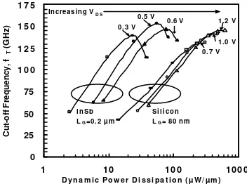
Figure 10. Extrapolated fT vs dynamic power dissipation (normalized to transistor width) for InSb QW transistors (solid) for LG = 0.2 µm and state-of-the-art Si nMOS transistors (open) for LG = 80nm.
and dynamic power dissipation performance of state-of-the-art Si nMOSFETs (80 nm LG) with the InSb
based quantum well FET’s (0.2 µm LG). The InSb
transistors provide equivalent high-speed performance (fT) at 5 to 10 times lower power dissipation per unit width compared to today’s advanced Si RF MOSFETs [2], as shown in Figure 10. This makes the InSb-based device technology a viable option for future generation ultra-high speed, very low power digital and RF applications. Future challenge is to scale the gate length of InSb transistors to compete with scaled CMOS transistors [3] for ULSI applications while maintaining the power advantage. Figure 11 shows the gate delay (CV/I) of InSb and state-of-the-art and research Si transistors as a function of gate length, showing the performance advantage at equivalent gate length.
0.1 1 10 100
1 1 0 1 0 0 1000 10000
Gate Length, LG ( n m )
Gate Delay, CV/I (ps)
S i M O S F E T s
I n S b Q W T r a n s i s t o r s NMOS
Figure 11. Transistor gate delay (CV/I) vs gate length for InSb QW transistors at VDS = 0.5 V bench -marked against state-of-the-art Si nMOS transistors.
6. Conclusion
In summary, we have demonstrated for the first time InSb quantum well transistors down to 0.2 µm gate length with comparable high frequency performance to today’s Si MOSFET’s but with 5-10 times lower dynamic power dissipation. This is enabled by lowering the supply voltage to 0.5 V due to 50X higher room-temperature mobility in InSb compared to silicon.
References
[1] T. Ashley, A. B. Dean, C. T. Elliott, R. Jefferies, F. Khaleque and T. J. Phillips, IEDM Technical Digest, p.751 (1997).
[2] K. Kuhn, R. Basco, D. Becher, M. Hattendorf, P. Packan, I. Post, P. Vandervoorn and I. Young, Symposium on VLSI Technology, June, (2004).