DEFENSE SPENDING
RADAR
on the
AI, robotics, big
data, cybersecurity, and
resilience top priorities page 8
APRIL 2018Also in
this issue
System integration
considerations for
heart rate sensing
designs p13
AI alters auto design
challenges p16
Modern portable
devices require a new
breed of LDOs p18
Advanced battery
packages empower
next-generation
systems p21
#
RED
FIT
n SKEDD Direct Plug-in Technology
n IDC Connection
n Solderless Solution
n Simple to Plug & Unplug
n Min. 10 Mating Cycles
n Reverse Polarity Protection
Perfect
match.
REDFIT IDC is a solderless reversible direct plug-in connector with SKEDD technology and insulation displacement connection. The SKEDD contacts are plugged directly into the plated
through-holes of a PCB.
A complete part and a potential error source is eliminated. This results directly in higher
process reliability, savings in space, material and process costs.
O N L I N E M U S T - R E A D S F E A T U R E S
8
COVER STORY Mil/Aero ElectronicsDefense spending opens door to system technology innovations
13
Discrete SemiconductorsSystem integration considerations for heart rate sensing designs
16
AutomotiveAI alters auto design challenges
P O W E R D E V I C E S S P E C I A L
18
LDO RegulatorsModern portable devices require a new breed of LDOs
21
BatteriesAdvanced battery packages empower next-generation systems
S H O W W R A P - U P S
23
Embedded WorldThe expanding IoT: a visit to Embedded World
25
APECAPEC’s growth reflects the health of the power industry
T O U C H P O I N T S
4
Viewpoint: Fluffing the cloud5
Publisher’s Perspective: Tribute to an American classic6
Outlook (Technology News):6 The key to smarter, faster AI likely found by modeling moth brains
6 Physicists to build laser so powerful it could rip apart fabric of space
27
Product Trends: Packaging, Cabinets & Enclosures29
Product Roundup: Electromechanical Components31
New Products:31
Power Sources
32
Packaging & Interconnections
32
Product Mart14
SCAN TO DOWNLOAD EP CALCULATOR APP:
Google’s new quantum processor aims to outper-form supercomputers http://bit.ly/2FuOS7U
Battery sensor allows for Li-ion batteries to be charged five times faster http://bit.ly/2FuOAhs
10 tips on how to properly document a design so others can follow http://bit.ly/2FpMJ18
EDITORIAL STAFF
Bolaji Ojo . . . .Global Editor-in-Chief
Richard Quinnell . . . .Editor-in-Chief,
[email protected] • electronicproducts.com
Majeed Ahmad Kamran . . . . .Contributing Editor
Patrick Mannion . . . .Contributing Editor
Alix Paultre . . . .Contributing Editor
Lori O’Toole . . . .Chief Copy Editor
Nicole DiGiose . . . .Technical Content Manager
Max Teodorescu . . . .Digital Content Manager
Pam Fuentes . . . .Business Planning Analyst
Giulia Fini . . . .Graphic Designer
Giulia Fini . . . .Cover Design
Lauren Heller . . . .Production Designer
Subscriber Service 1-866-813-3752 Subscriber Service Fax 1-847-564-9453 Reprints (Wright’s Media) 1-877-652-5295
Published by AspenCore
1225 Franklin Avenue, Suite 400 Garden City, New York 11530 TEL: 516-667-2300 • FAX: 516-667-2301
Victor Alejandro Gao
Chairman
Greg Rivera
Group Publisher Electronics Group
Electronic Products Magazine (USPS 539490) (ISSN 0013-4953)— Published monthly by AspenCore, 1225 Franklin Avenue, Suite 400, Garden City, NY 11530. Periodicals postage paid Garden City, NY and additional mailing offices. Electronic Products is distributed at no charge to qualified persons actively engaged in the authorization, recommendation or specification of electronic components, instru-ments, materials, systems and subsystems. The publisher reserves the right to reject any subscription on the basis of information submitted in order to comply with audit regulations. Paid subscriptions avail-able: U.S. subscriber rate $65 per year, 2 years $110. Single issue, $6.00. Information contained herein is subject to change without notice. No responsibility is assumed by the publisher for its accuracy or completeness.
Postmaster: Send address changes to Electronic Products, PO Box 489, Skokie, IL 60076-0489.
Phone: 847-559-7317
©2018 by AspenCore. ALL RIGHTS RESERVED Publications Mail Agreement Number 40012807.
Return Undeliverable Canadian Addresses to: Station A PO Box 12, Windsor, ON N9A 6J5
The right AC power
SOLUTION... at the
right price
Behlman has an ultra-reliable AC power supply or frequency converter that can
be configured for your exact needs.
Our rugged rack-mounted and portable units
deliver AC power at a low cost per watt – making us the choice for military and
industrial applications for over 60 years.
: 631-435-0410 : [email protected] : www.behlman.com
BEHLMAN
AC
POWER SOLUTIONS
>
RUGGED
>
ADAPTABLE
>
FLEXIBLE
>
MODIFIABLE
>
RELIABLE
The
Power Solutions
Provider
>
Avionics & aircraft 400Hz
>
Frequency conversion (50Hz, 60Hz
or 400Hz)
>
Production test
>
Facility power
>
Oil & gas exploration
>
Railroad signaling
>
Simulators & trainers
>
Airborne, shipboard, ground
T
he electronic design engineering field is a fantastic place to be at any given point and especially so in these modern times. The past two decades saw the groundwork laid for these exciting times in technologies likeorganic LEDs, wide-bandgap semicon-ductors, and the digital infrastructure. These and other advanced core technol-ogies enable and empower new solutions to serve existing application spaces and create and develop new ones.
This synergistic development aspect of electronic design was very appar-ent these past weeks at the APEC and Embedded World shows as engineers from around the globe came together in San Antonio, Texas, and Nuremberg, Germany, to exchange ideas and look at the latest in embedded systems.
The booths at both events were crammed with the latest solutions avail-able for applications both mature and speculative, and at each (some visitors, including me, bounced between both), there was a buzz of activity as company reps and visitors played with the demon-strations and bounced ideas off of one another. The energy was palpable at each of the venues, and the energy of all of those people dealing with one another in these public marketplaces was palpable.
In this issue, we’ve pulled together some very cool examples of the latest technologies from both shows, and we hope this foments new ideas for new solutions with you. One of the notable aspects of any new technology is that any given group of engineers will tell you sev-eral more applications than you thought of when developing it, and the number and quality of these new technologies are providing the foundation of the remak-ing of society.
The cloud and IoT are shaping society in fundamental ways, and you are the ones shaping the devices in it and the infrastructures supporting it. Every de-vice that you make is a voice in the great chorus of development moving society forward, and these exhibitions are the concert halls. One positive aspect of Em-bedded World, for example, was the fact that most booths contained functional demonstrations of technology and not just displays of components and parts.
In the area of wireless, one of the trends that we observed was the final filling in, or in the words of the headline, the “fluffing out” of the cloud. There are a lot of wireless devices using wired or sub-gigahertz proprietary wireless systems, for example, and bringing them into the IoT is the true “final mile” of the cloud. Solutions shown ranged from multi-protocol wireless modules and
Fluffing the cloud
N
EW YORK — American readers of this column are prone to recognize the name E.B. White, a 20th-century author best known for his children’s books such as “Stuart Little” and “Charlotte’s Web.” A resi-dent of this great American city, White was also a prolific columnist for the classic humor, literature, and journal-ism magazine The New Yorker. And in a prose entitled “Unwritten” in April 1930, White observed in his signature self-deprecating style that the work of a writer always represented a choice — the choice of what to write and what not to. Which brings me to the subject of our column this month: Why does a journalist write at all?At ASPENCORE, our editorial mis-sion is to bear witness and to cele-brate human achievement as manifest through advancement in technology and engineering. While every one of our journalists makes their own personal choice as to why and what they write, as a publishing house, we encourage an intention to affirm or, if the writing starts out decrying an inju-ry or injustice on behalf of our readers, that by the end, it arrives at a construc-tive juncture. Sometimes, that takes the form of questioning a dubious claim in a manufacturer’s new product introduction campaign. Other times, it could be the critique of a business trend we believe is over-hyped, a tech-nical achievement that is under-recog-nized, or an important workplace issue that would not have found its voice had it not been for the help of these pages.
Of course, a great deal of how this mission is achieved is left intentionally undirected and uncoordinated
be-tween the house and our writers. As a gentle reader wrote in response to this column last month, today’s publishers face a pivotal task to transform the economics of publishing so the im-portant reporting can be done without fear of loss of funding, which we have seen happen to some of our fellow
publishing houses in the industry. And yet as much as ASPENCORE as a com-mercial concern must make money, we strive even harder to always make sense. To achieve this duo of aims, at
ASPENCORE, we rather like the good old system at The New Yorker, as de-scribed by White in another column:
The writers write as they please, and the magazine publishes as it pleases. When the two pleasures coincide, something gets into print. When they don’t, the reader draws a blank. And you, the reader, are here to judge both the house and our writers on our re-spective merits. This is what editorial independence means to us.
While we are on the subject of editorial policy, we expect to share some exciting news soon about how we will extend our remit this year to
introduce both more depth and more diversity to the topics covered in our titles. We will give you a snippet of our redesign efforts, with a greater focus on longer, less frequent, but more thought-provoking pieces that delve into an issue without the pressures of a daily publishing cadence. To find out more, please check back in this column next month.
By the time these words go to print, many of our readers will be wheels-up to a productive conference in Münich, Las Vegas, or Shanghai or will have just returned. Here is to safe and pleasant journeys for all on the road. As ever, if you have a comment or want to whis-per us a story tip, you can find me at
[email protected], or contact your favorite ASPENCORE writer directly. From all of us at ASPENCORE, thank you for your support. ☐
Tribute to an American classic
In this month’s perspective, our publisher, Victor Gao, pays tribute
to an American classic and delves into our proudly old-fashioned
journalistic values
BY W. VICTOR GAO
Publisher and Managing Director The ASPENCORE Group
At ASPENCORE, our editorial mission is to bear witness and to
celebrate human achievement as
manifested through advancement in
technology and engineering ... and
you, the reader, are here to judge
both the house and our writers on
our respective merits. This is what
editorial independence means to us.
IM
PUBLISHER’S PERSPECTIVE
5
The key to smarter, faster AI likely
found by modeling moth brains
R
esearchers at the Univer-sity of Wash-ington have devel-oped a relatively simple neural network that mimics biological neural systems. Theperformance of the new neural-network model points to the possibility of building AIs that are less complex yet far more effi-cient at learning because of it. At the same time, the research, published in the arXiv repository, yielded new insight into how living creatures learn — or at least how some creatures learn some things.
The most common path to emulate the effectiveness of biological neural systems has been to create increasingly complex artificial intelligences with increasingly complicated machine-learning capabilities. Biological systems that outperform AIs sometimes aren’t all that complex, however, and living creatures often learn far more quickly than AIs using significantly fewer experiences to learn than AIs require data sets.
Starting with these observations, UW researchers resolved to devise a relatively simple neural-network model that mimics the relatively uncomplicated structure of a moth’s neurological system.
The University of Washington has been analyzing insect biology for decades; this research team chose moths because UW labs have already thoroughly mapped their neurological systems. They already knew that moths can learn smells after experi-encing them only a few times. Despite the relative simplicity, however, it remained unclear precisely how moths’ neurological systems worked when learning.
Most neural networks operate on the principle of backpropagation. With this technique, the weights between neurons (essentially the strength of the connection between them) are constantly recalculated through a process of feeding outputs back into the system so that inputs and outputs can be compared and adjusted against each other.
Biological systems rarely do anything like this. Instead, they are commonly organized as feed-forward cascades.
The beginning of the cascade in hawk moths is a set of about 30,000 chemical receptor neurons (RNs), which feed signals into an antennal lobe (AL). The AL contains roughly 60 isolated clusters of cells (called glomeruli — it pays to enhance your word power!), each of which focuses on a single odor stimuli feature. The AL, the researchers say, is inherently noisy. The researchers liken the AL to a pre-amplifier, “providing gain control and sharpening of odor representations.”
Signals from the AL are forwarded to a structure called the mushroom body (MB). The MB contains roughly 4,000 cells (Kenyon cells) associated with forming memories. Signals go through two more ancillary structures (each numbering in the tens of cells), the function of which is believed to be to read out the signals from the MB. These sparser structures act as noise filters, the researchers wrote. Noise isn’t eliminated but is sufficiently reduced for the purpose of effective learning.
The process does not work at all without octopamine, described as a neu-romodulator. Release of the chemical is triggered by a reward — for example, the moth finding sugar to consume. When a
moth finds a reward, the octopamine that is released stimulates enhanced activity in the AL and MB. The practical effect of this enhanced activity is to strengthen the connections between correlated neurons in the moth’s neurological system. The mechanism is called Hebbian learning; the extent to which the strength of neuro-nal connections can be changed is called Hebbian plasticity.
The UW researchers built a mathemat-ical model that mimics all of this, and their neural models of moths learned quickly with minimal simulated odor inputs. Their results are similar to the behavior that they observe in the moths, strongly suggesting that they have an accurate model.
If so, that will have ramifications both for biology and for neural networks.
That the behavior of the model was so similar to that of actual biological systems encouraged the researchers to expect that they might now have a clearer understanding of the mechanisms at work in living creatures. The olfactory/neuro-logical systems of moths are structurally similar to those of many other creatures, the researchers noted.
Their work also suggests a new path to explore for machine learning. “Specifically,” they wrote in their paper, “our experiments elucidate mechanisms for fast learning from noisy data that rely on cascaded net-works, sparsity, and Hebbian plasticity.”
Brian Santo
A
vacuum might not be empty at all; it might only seem empty on balance. That balance would be between electrons and their anti-matter counterparts, positrons. According to theory, any vacuum is filled with such electron-positron pairs. These pairswould be undetectable because they wouldn’t interact with anything — with the possible exception of the beam from a 100-petawatt laser. Which is one of the reasons why Chinese researchers are about to begin building a 100-PW laser.
These researchers propose to pulse
Physicists to build laser so powerful
it could rip apart fabric of space
IM
A
GE
: SHUT
TERST
OCK
an incredibly powerful beam for a few trillionths of a second through a vacuum with the expectation that it will induce elec-tron-positron pairs to break apart. Positrons are ephemeral, but the electrons would remain. It would look like producing some-thing out of nosome-thing. The proposed process is being described as “breaking the vacuum.”
The formula E=MC2 suggested two things. One is that mass can be turned into extraordinary amounts of energy. Scientists followed that lead in a number of directions, including the devel-opment of the atomic energy. The formula also suggests that it’s possible to translate energy into mass, though doing so is consid-ered significantly harder. Breaking the vacuum would be a rare instance of it.
The Shanghai Institute of Optics and Fine Mechanics in China currently holds the record for the most powerful laser. In 2016, the Shanghai Superintense Ultrafast Laser Facility (SULF) achieved a burst of 5.3 PW. The institute is currently preparing to nearly double its record by using SULF to emit a 10-PW pulse by the end of this year.
It is also planning to build a 100-PW laser called the Station of Extreme Light (SEL), which could come online as early as 2023. Photon energy from the device could reach 15 keV.
European researchers were thinking about building a 200-PW laser but have held off even planning such a beast until they turn on a 1-PW laser in Prague this year and then build two more facilities that would take intermediate steps toward 100 PW or more, reported Science.
Russia is building the infrastructure to support a proposed 180-PW laser called the Exawatt Center for Extreme Light Studies (XCELS). Japanese researchers, who held the record with a 2-PW pulse before the Chinese eclipsed them, have proposals for a 30-PW device, according to Science.
Breaking the vacuum would be spectacular, but high-en-ergy lasers could be useful in other applications as well. They have been used for particle acceleration, inertial confinement fusion, radiation therapy, and for secondary-source generation of X-rays, electrons, protons, neutrons, and ions, according to physicists at Cambridge University. A paper that they wrote in 2015 explains the different types of high-energy lasers. China’s SEL would be an OPCPA laser.
Brian Santo
OUTLOOK
7
T
he U.S. Department of Defense’s (DoD’s) 2018 National Defense Strategy (NDS) said it clearly: “Our backlog of deferred readiness, procure-ment, and modernization requirements has grown in the last decade and a half and can no longer be ignored. We will make targeted, disciplined increases in personnel and platforms to meet key capability and capacity needs.” With that in mind, Congress increased the FY 2018 defense budget to $700 billion — an increase of $108 billion.This article will lay out some of the areas where that budget will be spent and what areas may present opportunities for designers to innovate to close current and future technology gaps.
AI, big data, and robotics critical
but need to be affordable
The technological priorities called out in the NDS will drive a significant increase in R&D spending to close technology gaps in advanced computing, artificial intelligence (AI), and autonomy and robotics. Among the priorities for mod-ernizing key defense capabilities cited in the NDS that commercial off-the-shelf (COTS) vendors are well-positioned to support are:
• New investments in cyber-defense and the continued integration of cyber-ca-pabilities into the full spectrum of military operations
• Investments in C4ISR to develop resil-ient, survivable, federated networks and information ecosystems
• Advanced autonomous systems, AI, and machine learning.
For developers of military embed-ded COTS electronics solutions, this additional spending promises increased support for technologies that address
resilience, lethality, and readiness. Designers of defense and aerospace systems and platforms desire to contin-uously introduce advanced technology that provides the warfighter with an indisputable advantage in the battlefield. These technologies range from sensors, computing, and networking to electro-mechanical systems.
However, advanced technology by itself isn’t enough. It also needs to be affordable, reliable, and sustainable. The warfighters’ lives depend on the
tech-nology, and history has proven that if a soldier can’t trust their technology, they will abandon it.
New spending on advanced com-puting will result in improvements for leveraging big data analytics, enabling the warfighter immediate access to all of their critical information. Such access will require the use of cloud-computing technologies to enable data access by any device, wherever the soldier is located, at any time it’s desired. More than that, to bring the power of machine learning (ML) for AI to the network edge will require far greater local processing capa-bility in order to deliver real-time data and solve the cloud’s inherent latency and bandwidth limitations.
Investments in AI and ML will provide capabilities that disrupt battle-field applications such as intelligence,
surveillance, reconnaissance (ISR), and electronic warfare (EW). Support-ing these new capabilities will require advances in heterogeneous high-perfor-mance embedded computing (HPEC) technologies.
Embedded systems for use on semi- and fully autonomous unmanned platforms, whether on the ground, in the air, or at sea, will require the development of low-power, ultra-small form-factor (USFF) processing, networking, full-motion video, and data-storage solutions. It’s estimated, for example, that a fully autonomous car will require 50 to 100 times the com-pute power needed to support today’s advanced driver-assistance systems.
The overarching investment strategy described in the DNS is to bring these advanced technologies to the battlefield in order to provide a force multiplier that gives warfighters a strategic and tacti-cal advantage over the adversary. That said, it’s not enough to just deploy new technologies, it’s also necessary to ensure that those technologies are brought into the battlefield in a way that protects and secures them with the resiliency that they need to survive enemy attempts to dis-able or disrupt their intended operation.
Ensuring operational effectiveness
in the field: GPS
The new technologies will provide new capabilities upon which the warfighter will surely become dependent. As such, they must also feature the defenses needed to ensure that their network and computing environments are protected against adversaries and so remain opera-tionally effective.
An example of an advanced tech-nology upon which the warfighter has become dependent is GPS. When intro-duced as part of the DoD’s Second Offset strategy in the mid-1970s, GPS provided a significant advantage in the battlefield thanks to its ability to deliver accurate
Defense spending opens door to system
technology innovations
BY MIKE MACPHERSON Vice President, Strategic Planning, Curtiss-Wright Defense Solutions
www.curtisswright.com
position, navigation, and timing (PNT) data.
This technology was essential for applications such as precision-guided weapons like the Tomahawk missile. Over the years, it’s become clear that our dependence on GPS also makes it a vul-nerability. In environments in which GPS is denied or disabled, all of the weapons that depend on it are made ineffective. To counter that vulnerability and threat, an assured PNT (A-PNT) solution must be available that is able to operate even in a GPS-denied environment. New cost-ef-fective and accurate COTS-based A-PNT technologies will enable the deployment of cost-effective, rugged solutions for GPS-denied environments.
Making AI and autonomous
vehicles resilient
The development of new technologies based on AI will enable man-to-machine teaming solutions that deliver a significant advantage in the battlefield. Leveraging AI, autonomy, and robotics will result in machines that can operate independently, whether as an individual entity, paired with other machines in applications (such as a swarm configuration of drones), or in a soldier-machine interface in which the machine has its own autonomous capabil-ity augmenting the warfighter.
An example of the latter is an auton-omous ground combat “mule” able to relieve the warfighter’s personal burden of carrying batteries, chargers, ammuni-tion, etc. By reducing the weight in the warfighter’s backpack, these small auton-omous vehicles will significantly increase the soldier’s ability to fight.
Likewise, the use of autonomous aerial vehicles to deliver logistics equipment
or to locate IEDs will reduce the warfighter’s exposure to risk and improve their lethality. On the other hand, as these new solutions become common, adver-saries will strive to find ways to attack and disable them. For example, one strategy for countering a learning machine is to spoof it with false information, forcing it to produce an incorrect answer.
Improving resilience, another key goal of the DNS, will ensure that de-ployed systems have the ruggedness and reliability to survive harsh environments and the security to protect against enemy attempts to exploit their vulnerabilities.
Autonomous vehicles, such as mine detectors, can keep the warfighter out of harm’s way, but that autonomy needs to be trusted. For this, the system requires the resilience, or self-resilience, that ensures that it’s reliable and can’t be easily disabled.
A machine can be manual, semi-au-tonomous, or fully autonomous. In each of these states, the higher the level of
autonomy, the more the machine needs self-resilience. When a machine is fully manual, the warfighter provides the resil-ience. In the case of a semi-autonomous system, resilience is shared between the operator and the machine. In a fully autonomous system, resiliency depends
completely on the expert systems built into that machine.
Autonomous systems need
resilience and security
To be able to confidently depend on fully autonomous systems will require invest-ments in technologies that provide both resilience and security.
An example of resiliency is found in safety-certifiable avionics systems for manned or unmanned military aircraft. To operate safely over do-mestic airspace, these platforms are increasingly required to meet DO-254 hardware and DO-178 software certi-fication for specific Design Assurance Levels (DALs) recognized by aviation authorities around the world, such as the FAA in the U.S., the Canadian Transport Board, and EASA in Europe and the U.K. While safety certification is handled at the platform level, the electronic modules used to build out avionics subsystems must be supported with comprehensive data artifacts. His-torically, modules for safety-certifiable subsystems were costly custom designs that took years to design and millions of dollars to develop.
In recent years, a new class of cost-ef-fective DO-254-certifiable COTS boards has become available, greatly speeding
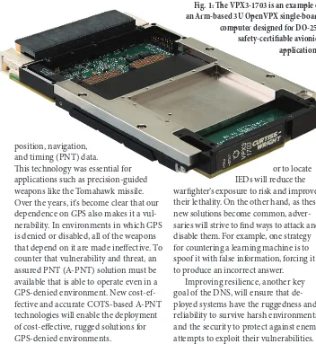
and lowering the cost of
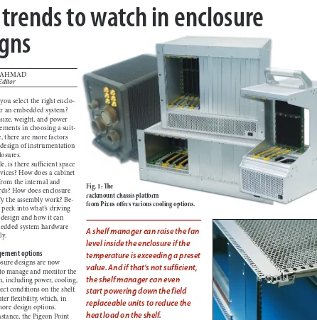
inte-Fig. 1: The VPX3-1703 is an example of an Arm-based 3U OpenVPX single-board computer designed for DO-254 safety-certifiable avionics applications.
grating safety-certifiable applications.
The preferred processor architecture for these COTS modules has been the Power Architecture family of devices being that Intel processors only support DO-254 up to the DAL C level.
As NXP shifts its focus from devel-opment of new Power Architecture pro-cessors toward Arm-based propro-cessors, designers of safety-certifiable systems are increasingly turning to Arm-based solutions. Arm processors support D0-254 up to the most stringent and critical level, DAL A, and also provide the additional benefit of very low power dissipation. The VPX3-1703 3U Open-VPX is a good example of an Arm-based single-board computer (SBC) (Fig. 1). It is designed for DO-254 safety-certifiable avionics applications.
The concepts of resilience and trusted systems refer not only to safety but also to data and hardware security. Great strides are being made today to enable COTS systems with anti-tamper technol-ogies, cybersecurity, and protection of
data-at-rest and data-in-motion. For example, the Data Transport System (DTS1) network attached storage (NAS) device supports cost-effective two-layer encryption (Fig. 2). The DTS1 is also easily integrated into net-work-centric systems.
Design for tech-savvy warfighters
The soldiers now using this equipment are digital natives — almost born with modern technologies in their hands. Along with this technological adept-ness comes a high level of assumption and expectation.
Today’s warfighter expects and de-pends on access to technologies as good as or better than what they have at home, such as an iPhone X, and social net-working services to enable information sharing in real time in the battlefield. All of today’s internet resources, whether searching on Google or asking questions of Siri or Alexa, are only years away from being available to the warfighter. As we increasingly bring reliable networked
desktop computing, mobile platform, and social media capabilities to the warfighter to enable “network-centric warfare,” the network itself has become a key component of our ability to operate.
This technological adeptness can also be leveraged to address readiness, an area of military spending that has been relatively underfunded in recent years. Advanced computing can be brought to bear for training and mis-sion-planning and exploiting technolo-gies developed for the gaming industry to provide sophisticated, realistic scenarios and experiences.
By having training embedded in the actual deployed platform, warfighters will be able to train while they operate without requiring a dedicated training location. Realistic simulation can be done virtually, providing, for example, the ability to train for a specific mis-sion while en route.
Contain costs with open systems
Many of the technologies discussed
above will benefit from the use of open systems, which reduce design risk and greatly speed time to deployment. The use of open systems also delivers significant cost reductions. Affordability results from competition and provides an alternative to expensive proprietary solutions.
Another key benefit of open systems is seen in technology insertions. Open systems enable the rapid insertion of new technology by defining an inter-face between different entities whose advancements progress at different rates. An open-systems interface, such as the OpenVPX system architecture, functions as a differential that enables the use of technologies that evolve out of synchrony.
For example, the fire control com-puter algorithms used in a main battle tank to handle ballistic solutions tend to evolve at a very slow relative rate with very little change from one year to the next. In comparison, the underlying processing technology used to run those algorithms progresses much faster. On the flip side, with EW as the example, the very sophisticated algorithms used to help identify a specific signal of interest in the noise of the electromagnetic spec-trum have developed at a much faster rate than the processors that are used to run them in deployed systems.
The result is that the most advanced EW algorithms wait for processor
bandwidths to catch up in order for them to be put to use. The use of open-standard interfaces enables the processing technology and the algo-rithms used on deployed platforms to advance at different rates.
Innovation opens door to vulnerabilities
For every new opportunity and tech-nological leap forward, there is likely to be an associated vulnerability that emerges. While investing in the tech-nologies sought by the DoD in order to enable new capabilities and increase force lethality, technology providers must also invest in mitigating against those vulnerabilities.
The use of COTS-based open sys-tems provides a cost-effective approach to bringing these capabilities to the warfighter quickly and with the least risk. To bring the powerful benefits of advanced computing, AI, auton-omy, and robotics to the warfighter, COTS solutions must be designed and packaged to meet the environ-mental and usage requirements of the battlefield. The equipment must be dependable and operate while exposed to extreme environmental conditions. The technology must also be designed and packaged to ensure safe and secure operation. Care must be taken to en-sure safe operation without requiring burdensome safety precautions. System
designers need to design and package next-generation COTS solutions to eliminate vulnerabilities to adversarial access or attack, including cybersecu-rity and protection against reverse-en-gineering to prevent physical access intended to disrupt operation.
It’s essential that these new technol-ogies assure the security of the defense systems and critical information during development and operation.
Another area of great importance is testing, which must be done to ensure that deployed COTS solutions are reliable and deliver error-free operation throughout their useful life.
Conclusion
The DoD and warfighters depend on trusted and proven sources of supply, and Congress has made available the funds to make this happen. Now it’s up to designers and other innovators to realize the full promise of new technol-ogies outlined here, just as examples. For sure, the COTS approach provides a proven alternative to costly, closed proprietary system architectures, speeds deployment, and ensures that critical technologies remain readily available over the lifecycle of their use. How tech-nologists build upon and apply it for next-generation battlefield deployments with more tech-savvy warfighters will be interesting to watch. ☐
•
Dual inductors in a single shielded package saves board space
•
Very low coupling coefficient (k<0.001) minimizes crosstalk
•
Excellent inductance vs. current linearity up to 10 Amps
•
Economical solution for a wide range of audio applications
UA801x Series Dual Inductors
for Class-D Output Filters
D
esigning an optical heart rate monitoring (HRM) system, also known as photoplethysmography (PPG), is a complex and multidisciplinary undertaking. Design factors include human ergonomics, signal processing and filtering, optical and mechanical design, low-noise signal receiving circuits, and low-noise current pulse creation.Wearable manufacturers are increas-ingly adding HRM capabilities to their health and fitness products, which is helping to drive down the cost of sensors used in HRM applications. Many HRM sensors now combine discrete compo-nents such as photodetectors and LEDs
into highly integrated modules. These modules enable a simpler implementa-tion that reduces the cost and complexity of adding HRM to wearable products.
Wearable form factors are steadily changing as well. While chest straps have
effectively served the health and fitness market for years, HRM is now migrating to wrist-based wearables. Advances in optical sensing technology and high-performance, low-power processors have enabled the wrist-based form factor to be viable for
System integration considerations for
heart rate sensing designs
When it comes to optical
HRM designs, developers
have a choice of doing it all or
purchasing it all
BY MORRIE ALTMEJD Senior Staff Systems Engineer, Silicon Labs
www.silabs.com
Fig. 1: Principles of operation for optical heart rate monitoring.
Fig. 2: The basic electronics required to capture optical heart rate.
Excitation signal Typically green (525 nm ), 100 µs long pulses repeated at 25 Hz
Attenuated and pulse modulated light
Optical blocking is critical to prevent the unmodulated excitation signal from overwhelming the desired signal
Skin
Sensor Photodiode Green LED
Subdermal Tissue
ELECTRONIC PRODUCTS • electronicproducts.com • APRIL 2018
FEATURE
13
many designs. The HRM algorithms have also reached a level of sophistication to be acceptable in wrist form factors.
Other new wearable sensing form fac-tors and locations are emerging — such as headbands, sport and fitness clothing, and earbuds. However, the majority of wearable biometric sensing will be done on the wrist.
HRM design fundamentals
No two HRM applications are alike. System developers must consider many design tradeoffs: end-user comfort, sensing accuracy, system cost, power consumption, sunlight rejection, how
to deal with many skin types, motion rejection, development time, and physical size. These design considerations impact system integration choices: whether to use highly integrated modules or architectures incorporating more discrete components.
Fig. 1 shows the fundamentals of mea-suring heart rate signals, which depend on the heart rate pressure wave being optically extracted from tissue. It displays the travel path of the light entering the skin. The expansion and contraction of the capillaries — caused by the heart rate pressure wave — modulate the light signal injected into the tissue by the green LEDs.
The received signal is greatly
attenu-ated by the travel through the skin and is picked up by a photodiode and sent to the electronic subsystem for processing. The amplitude modulation due to the pulse is detected, analyzed, and displayed.
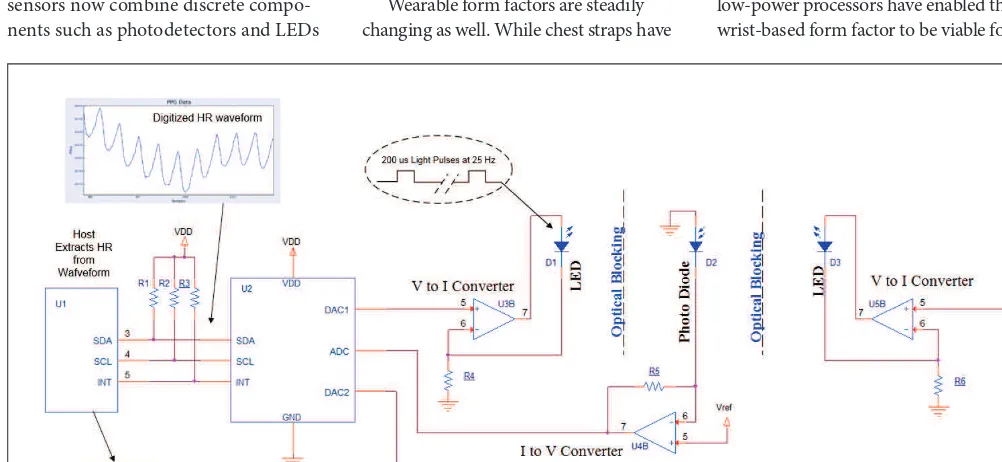
A fundamental approach to HRM sys-tem design uses a custom-programmed, off-the-shelf MCU that controls the puls-ing of external LED drivers and simul-taneously reads the current output of a discrete photodiode. Note that the current output of the photodiode must be con-verted to voltage to drive analog-to-digital (A/D) blocks. The schematic in Fig. 2
shows the outline of such a system. Here, it’s worth noting that the I-to-V converter creates a voltage equal to VREF at 0 photodiode current, and the voltage decreases with increasing current.
HRM building blocks
The current pulses generally used in heart rate systems are between 2 mA and 300 mA, depending on the color of the subject’s skin and the intensity of sunlight with which the desired signal needs to compete. The infrared (IR) radiation in sunlight passes through skin tissue with little attenuation, unlike the desired green LED light, and can swamp the desired signal unless the green light is very strong or unless an expensive IR blocking filter is added.
Generally speaking, the intensity of the green LED light, where it enters the skin, is between 0.1 and three times the intensity of sunlight. Due to heavy attenuation by the tissue, the signal that arrives at the photodiode is quite weak and generates just enough current to al-low for a reasonable signal-to-noise ratio (SNR) — 70 to 100 dB — due to shot noise even in the presence of perfect, noise-free op-amps and A/D converters.
The shot noise is due to the finite number of electrons received for every reading that occurs at 25 Hz. The photodiode sizes used in the design are between 0.1 mm2 and 7 mm2. Howev-er, above 1 mm, there are diminishing returns due to the effect of sunlight.
The difficult and costly function blocks to implement in an optical heart rate system design, as shown in Fig. 2, are the fast, high-current V-to-I converters
Fig. 3: An integrated heart rate sensor requires only external LEDs.
that drive the LED, a current-to-volt-age converter for the photodiode, and a reliable algorithm in the MCU that sequences the pulses under host control. A low-noise LED driver — featuring 300 mA and 75–100 dB SNR — that can be set to very low currents down to 2 mA while still creating very narrow light pulses down to 10 µs is an expensive block to achieve with discrete op-amps.
The narrow pulses of light down to 10 µs, shown in Fig. 2, allow the system to tolerate motion and sunlight. Typically, two light measurements are made for each 25-Hz sample. One measurement is taken with LEDs turned off and one with LEDs turned on. The calculated differ-ence removes the effect of ambient light and gives the desired raw optical signal measurement that is insensitive to the flickering background light.
The short duration of the optical pulses both allows and requires a rela-tively strong light pulse. It is essential to stay brighter than the sunlight signal, which may be present and not allow the PPG signal carrier to be dwarfed by the sunlight signal.
If the sunlight signal is larger than the PPG carrier, then although it may be removed by subtraction, the signal can be so large that external modulation such as swinging an arm in and out of shadow can create difficult-to-remove artifacts. As a result, systems that use low-current LED drivers and large photodiodes can suffer severely from motion artifacts in bright-light situations.
Discrete vs. integrated design
Much of the desired HRM sensing func-tionality is available pre-designed and integrated into a single device. Packing most of this functionality into one piece of silicon results in a relatively small 3 x 3-mm package that can even integrate the photodiode itself.
Fig. 3 shows an example of a sche-matic with an optical sensor. This HRM design is relatively easy to implement. You just need to focus on the optical por-tion of the design, which includes optical blocking between the parts on the board and coupling the system to the skin.
While the approach shown in Fig. 3
results in a high-performance HRM solu-tion, it’s not as small or power-efficient as some designers would like. To achieve an even smaller solution, the LED die and the control silicon must be integrated into a single package that incorporates all essential functions, including the optical blocking and the lenses that improve the LED output. Fig. 4 illustrates this more integrated approach, based on a Silicon Labs Si117x optical sensor.
No external LEDs are required for this HRM design. The LEDs and photodiode are all internal to the module, which can be installed right below the optical ports at the back of a wearable product such as a smartwatch. This approach enables a shorter distance between the LEDs and photodiode than is possible with a dis-crete design. The reduced distance allows operation at extremely low power due to lower optical losses traversing the skin.
Integrating the LEDs also addresses the issue of light leakage between the LEDs and photodiode so that the designer doesn’t have to add optical blocking to the PCB. The alternative to this approach is to handle the blocking with plastic or foam inserts and special copper layers on the PCB.
There is one more part of an HRM design that developers don’t necessarily need to create: an HRM algorithm. This software block residing on the host pro-cessor is quite complex due to the signal corruption that occurs during exercise and motion in general. End-user motion often creates its own signal that spoofs the actual heart rate signal and is sometimes falsely recognized as the heart rate beat.
If a wearable developer or manufacturer doesn’t have the resources to develop the algorithm, third-party vendors provide this software on a licensed basis. It is up to the designer to decide how much integra-tion is right for the HRM applicaintegra-tion. The developer can simplify the design process and speed time-to-market by opting for a highly integrated module-based approach using a licensed algorithm.
Developers with in-depth optical sensing expertise, time, and resources may opt to use separate components — sensors, photodiodes, lenses, etc. — and do their own system integration and even create their own HRM algorithm. ☐
ELECTRONIC PRODUCTS • electronicproducts.com • APRIL 2018
FEATURE
15
A
rtificial intelligence (AI), electrification, and in-cab-in entertain-cab-inment are just some of the revolutionary changes underway for automobiles, causing a complete rethink of how an automobile should be designed and used. They’re also cause for designers to rethink their own role in the automotive design chain.From a semiconductor and components environmental per-formance point of view, the same rules apply, namely AEC-Q100, which has been around since 1994. This defines the temperature, humidity, and other reliability factors. Since 1994, however, much has changed, and soon, “auto” mobiles will start living up to their name, thanks in large part to advances in sensor integration, AI, Moore’s Law, and some people in remote regions making a living by tagging images to make smart systems more accurate.
For example, accurate labeling can make the difference between distinguishing between the sky and the side of a truck. Mighty AI is one company focused on ensuring accurate
tagging using teams of humans spread globally. According to its founder, S. “Soma” Somasegar, there is a large role for humans in this loop for a long time to come. “We’re not building a sys-tem to play a game; we’re building a syssys-tem to save lives,” said Mighty AI CEO Daryn Nakhuda.1
Getting to the point at which autonomous vehicles can be considered relatively safe for everyday use is an interesting challenge that has captured the imagination of automobile OEMs and electronic system designers and spurred innovations in sensors, processing, and communications.
For some time, it was believed that LiDAR would be the critical breakthrough technology that would enable auton-omous vehicles, but now, developers have realized that it’s a combination of every sensor input possible, including sonar, high-definition cameras, LiDAR, and radar, all to ensure accu-rate ranging and identification of objects. According to GM, the autonomous version of its Chevy Volt electric vehicle (EV) has 40 more sensors and 40% more hardware.
Lowering the cost and power consumption of that hard-ware, especially for advanced image processing, is one of many critical enabling factors for autonomous vehicles. To that end,
Dream Chip Technologies announced an advanced driver assistance system (ADAS) system-on-chip (SoC) for computer vision at Mobile World Congress (MWC) that greatly increases performance while lowering power consumption.
The ADAS SoC was developed in collaboration with Arm, ArterisIP, Cadence, GlobalFoundries (GF), and Invecas as part of the European Commission’s ENIAC THINGS2DO reference development platform. It was developed on GF’s 22FDX tech-nology to lower the power required for AI and neural network (NN) processing so that it can be embedded into a vehicle without the need for active cooling techniques, which can add weight, size, and cost while increasing the probability of failure.
The SoC uses Dream Chip’s image signal-processing pipe-line, Tensilica’s (Cadence) P6 DSPs, and a quad-cluster of Arm Cortex-A53 processors to get to 1 tera operations per second (TOPS) with a power consumption “in the single digits.”
Distributed vs. centralized sensor processing
The low-power performance of Dream Chip Technologies’ SoC at low power for image processing is critical, given that latency needs to be minimized to avoid incidents. The further that a ve-hicle can see, and the sooner that it can process what it sees, the safer a vehicle will become. However, as mentioned, there are many sensors required for reasonably intelligent decision-mak-ing, which raises the question of where and how all of those sensor inputs should be processed.
Sensor fusion techniques are well-known in applications such as drones, in which gyroscopes, accelerometers, and magne-tometers are managed in such a way that the benefits of each are accentuated and the negatives attenuated. How can this be done for autonomous vehicles with so many and varied sensors?
To tackle this, Mentor Graphics decided to work backwards and start with Level 5 autonomy in mind. Its approach is called DRS360 and it takes (fuses) raw sensor data from LiDAR, radar, and cameras and processes it to develop a 360-degree real-time view of vehicle surroundings. The centralized approach reduces latencies but does require a high level of centralized processing, which Mentor provides using Xilinx Zynq UltraScale+ MPSoC FPGAs with its advanced NN algorithms. The alternative is to do the image, LiDAR, or radar processing locally at the sensor and send the results upstream, but that approach doesn’t scale as efficiently as DRS360, nor does it take full advantage of rap-idly changing and evolving algorithms. The downside is a single point of failure, but built-in redundancies and good design can offset that.
The importance of automotive sensors is not lost on the MIPI Alliance, which is bringing its experience with defining sensor physical-layer interfaces on mobile handsets to the rapidly evolving automotive space. On Oct. 7, it announced the formation of the MIPI Automotive Working Group (AWG) to
AI alters auto design challenges
Getting to the point at which autonomous vehicles
can be considered safe for everyday use is a
challenge that has captured the imagination of
automobile OEMs, spurring innovations in sensors,
processing, and communications.
Automobile designers need to incorporate new approaches as change comes quickly
BY PATRICK MANNION
bring standardization to sensor interfaces to lower development costs, reduce testing time, and improve reliability. With its background in mobile devices, MIPI Alliance is also confident that it can help ensure that highly sensitive, mission-critical automotive applications suffer minimally from EMI.
Elec
trification of vehicles accelerating
Though often considered to be synonymous with autonomous vehicles, the move to electrification to replace the internal com-bustion engine (ICE) is moving at its own pace with different drivers. Primarily, electric vehicles with their large batteries are seen as a more sustainable form of transportation. However, that battery does add weight, up to 32% more versus an equiv-alent ICE vehicle, according to Dan Scott, market director for integrated electrical systems at Mentor Graphics.
The issue, then, is to minimize weight, which goes directly to cables, harnesses, and connectors. The other issue with elec-trical vehicles is the higher power requirements, with currents of up to 250 A at 400 V for a typical 1-KW battery implemen-tation. Such high currents cause more energy losses to heat generation, which is driving a move to 800-V power for EVs. This will also reduce the cable weight, as will other techniques, such as removing shielding on high-power cabling. McKinsey & Company tore down eight EVs just to see how they were differentiated, and power and thermal management proved to be an interesting factor with no convergence on power-train design approaches yet (Fig. 1).
However, there are trade-offs associated with that, said Scott, such as EMC issues. “Also, with things like regenerative braking, now you have power electronics, motor controls, and battery chemistry to consider, so you have to share that data between different tools,” said Scott. “This requires a much more holistic design approach.”
For this, Mentor developed its Capital software suite for electrical and wire harness design and layout for automotive and aerospace applications. The goal of Capital is to maintain a seam-less data flow from vehicle concept and electrical architecture
definition to wire harness manufacture and vehicle maintenance. “Capital excels at managing complex systems,” said Scott. “We’ve got generative design, where we can take basic archi-tectures and auto-generate wiring diagrams from that.” While Capital doesn’t pick the specific components required, Scott said that Mentor does have a design services team that can help with next-level design decisions.
Comfort and services replacing performance
As vehicles evolve toward autonomy, comfort, entertainment, and services are becoming seen as more differentiating factors than performance and road “feel.” Ford has recognized and championed this migration toward services, and Intel has long promoted the focus on data, both on the vehicle and on its usage.
How vehicles are being used is changing the business model, with younger users showing an affinity for a subscription model versus owning a vehicle. Also, they like to be both informed and entertained, which inspired Imagination Technologies to announce its PowerVR Series8XT GT8540 four-cluster IP for high-definition heads-up displays and infotainment. The GPU core can support multiple high-definition 4K video streams as well as up to eight applications and services simultaneously. ☐
Reference:
1. Nakashima, R. (2018, March 5). AI’s dirty little secret: It’s pow-ered by people. Retrieved from http://bit.ly/2G2w6G1.
Fig. 1: A teardown of eight EVs showed large differences in how power trains are designed and how thermals are managed.
IM
A
GE
: MCKINSEY
&
C
OMP
AN
Y
High-quality precision
stamping since 1986
Na Bob Precision Metal Industry Ltd Homepage: www.nabobind.com Email: [email protected]
* 200 pressing machines, Robotic arms and EDMs * 30 QC technicians perform IQC, IPC and QA * Clients in the US, Japan and Europe
EET201803_Na Bob.indd 3 2018/3/1 上午9:37
FEATURE
17
Automotive
I
n the long electric path from the power source — be it the AC line or the battery — to an electronic load, the low-dropout (LDO) regulator is often called upon to cover the “last mile.” Here, the noisy switching regulator steps aside in favor of the quiet LDO to power critical electronic loads. The LDO has been under constant renewal or evolution along with the rest of power management electronics. Over time, the LDO has not only become quieter but more reliable, accurate, fault-tolerant, powerful, and efficient, with a mix of features that adapt to the application at hand.Recent applications like miniature
wireless 4G base stations have challenged the already small LDO to become even smaller while packing more power. In this article, we’ll review the main features of an LDO while comparing a mod-ern CMOS LDO to an old bipolar workhorse. Subsequently, we’ll review how each LDO parameter helps solve a specific application problem. We’ll then introduce a new family of LDOs with features that enable further miniaturization, enhance fault tolerance, and support a broad range of modern applications.
LDOs have come a long way
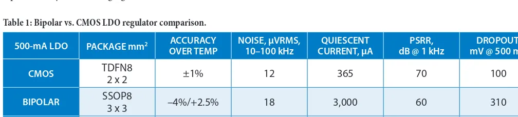
Table 1 compares the main features of a pioneering bipolar LDO regulator with an integrated PNP pass transistor (2.1- to 16-V in-put voltage) to a modern CMOS LDO with an integrated PMOS pass transistor (1.7- to 5.5-V input). As you can see from across all of the features listed, the CMOS LDO outperforms the old bipolar one by a factor ranging from 1.5 to 8 times!
The following LDO parameters are important for the applica-tion at hand:
Low noise and high PSRR. In wired and wireless
commu-nication systems, the LDO provides a clean power supply to sensitive analog circuits (PLL, VCO, RF). The LDO must
have good power-supply rejection ratio (PSRR) to isolate its load from its source, likely due to a noisy switching
regulator. Low spectral noise (VRMS/√Hz) will
mini-mize linearity degradation in the RF demodulator and phase noise in the PLL and VCO circuits.
Low power dissipation. While power dissipa-tion is the LDO’s Achilles heel, a 5-V, 500-mA
LDO with a 100-mV dropout (500 mA x 200 mΩ) will yield a respectable 98% efficiency
when used with a 5.1-V input (50-mW losses), rivaling some of the best switching regulators. Used properly, the LDO’s qualities can be ex-ploited without having to suffer its shortcomings.
Low quiescent current. In operation, the qui-escent current of an LDO will dissipate additional
power. A 4-mA quiescent current with a 5-V input (as shown for the bipolar LDO in Table 1) will dissipate 20 mW. This robs the
regula-tor of almost another whole percentage point of efficiency. The CMOS regulator, with only 365 µA of quiescent current, can re-duce this loss tenfold. This is significant because low quiescent current is as important as low dropout in portable applications. High output accuracy. Additional power dissipation can oc-cur due to an output voltage that is higher than nominal, even when within an acceptable range of tolerance. At 4% accuracy over 5 V and 500 mA, you will see a power dissipation increase of 4% x 5 V x 500 mA = 100 mW. This is as costly as the losses from the pass transistor of the previous case! This is inadequate for power-hungry portable applications.
Low leakage. Even while not in operation, the LDO needs to perform efficiently. Wearable devices are typically very small in size and must last a long time both in operation and on the shelf. Minimization of the size and power dissipation in both modes is crucial. While on the shelf in shutdown mode, the
Modern portable devices require a new
breed of LDOs
BY DIMITRY GODER, Director of Product Definition; KEN SALVI, Business Manager;
NAZZARENO ROSSETTI, Ph.D. EE Maxim Integrated
www.maximintegrated.com
Fig. 1. State-of-the-art low-dropout regulator: smaller than a drop of water.
Table 1: Bipolar vs. CMOS LDO regulator comparison.
500-mA LDO PACKAGE mm2 ACCURACY
OVER TEMP
NOISE, µVRMS, 10–100 kHz
QUIESCENT CURRENT, µA
PSRR, dB @ 1 kHz
DROPOUT, mV @ 500 mA
CMOS TDFN8
2 x 2 ±1% 12 365 70 100
BIPOLAR SSOP8
3 x 3 –4%/+2.5% 18 3,000 60 310
CMOS OVER BIPOLAR
device might need to last up to three years, which requires a very low leakage current.
New requirement: reverse-current protection.
Reverse-cur-rent protection is a new feature seldom found in available LDOs. In battery-operated equipment, the load is regulated typically via an efficient CMOS LDO with a MOSFET pass transistor that
car-ries a reverse-biased intrinsic diode between input and output. The reverse-current protection prevents the large reverse current that occurs when a buck regulator at the LDO input is shut off, shorting the input to GND. The discharge energy of a large LDO output capacitance through the LDO pass transis-tor’s intrinsic diode creates the damage. A low reverse current is tolerated. Above a set threshold (200 mA), the reverse current is completely blocked.
New requirement: Miniaturization. As seen in Table 1, little progress has been made in LDO packaging miniaturization. This is due, in part, to reliability concerns. In harsh environ-ments like automotive under-the-hood applications, lead-frame IC packages like the TDFN-8 are preferred because they have proven their high reliability over time. Lead-frame technology is inherently space-inefficient.
On the other hand, in consumer and wireless communica-tions applicacommunica-tions, size is a major concern. Fortunately, these environments are relatively benign and stress-free, opening opportunities for innovation.
Can we preserve all of the progress made by LDO electrical parameters and add additional features like fault tolerance with reverse-current protection and miniaturization for wireless appli-cations? A new family of LDOs positively answers this challenge.
A state-of-the-art solution
The excellent parameters shown in Table 1 for the CMOS
LDO are applicable for the MAX38902A/ MAX38902B/ MAX38902C/MAX38902D family of LDO regulators. Going even further, this new family solves the miniaturization prob-lem by providing an option of wafer-scale packaging tech-nology, resulting in minimal PCB space usage. In addition, it solves the reverse-current protection problem with a novel implementation of the LDO power train. Let’s review these innovations in more detail:
Wafer-scale packaging. Miniature 4G base stations are small enough to fit in a backpack and are still very powerful. Here, the LDO that powers the RF section must be small and power-ful, delivering hundreds of milliamperes. The C and D versions of this newer LDO family adopt wafer-level packaging (WLP)
technology for increased miniaturization. Fig. 2 illustrates how
the 500-mA LDO regulator, in a WLP-6 package, occupies roughly one-fourth the space of the TDFN-8 footprint (and one-sixteenth of the SOT23-5 of Fig. 4). The WLP-6 solution is
well-suited for applications that require minimal PCB space.
Reverse-current protection. The pass element (T1 in Fig. 3)
is a low RDSON p-channel MOSFET transistor. The internal circuitry senses the MOSFET drain-to-source voltage and, in addition to driving the gate, keeps the body diode reverse-bi-ased. This additional step allows the device to behave like a true open switch when its polarity is reversed (LDO OUT 10 mV higher than LDO IN). A positive drain-to-source voltage, under proper drive (CONTROL), turns the MOSFET “on,” with current flowing in normal mode while the body diode is again reverse-biased.
This innovative feature protects the load and the LDO from
Fig. 2: MAX38902C/D WLP-6 package advantage.
Fig. 3: MAX38902A/B/C/D reverse-voltage protection.
Fig. 4: MAX38902A/B TDFN-8 package advantage.
WLP-6 1.22 x 0.82 x 0.84 mm
TDFN-8
2.0 x 2.0 x 0.8 mm SOT23-5 2.8 x 2.8 x 1.2 mm
TDFN-8 2.0 x 2.0 x 0.8 mm
SPECIAL
19
Power Devices
accidental input shorts, making the system more fault-tolerant.
High-reliability applications. Industrial and automotive
appli-cations are characterized by a wide operating temperature range. Here, a lead-frame package, more tolerant of temperature-in-duced PCB surface mechanical stress, may be preferred. In this case, a modern TDFN package (A and B versions) provides a solution that is roughly half the footprint and two-thirds the height of a more traditional SOT23-5 or similar package (Fig. 4).
Low noise performance.Fig. 5 shows the spectral noise
density of this family of devices. With a figure of merit as low
as 30 nV/√Hz), it is an excellent choice for many low-noise applications.
High PSRR performance. Fig. 6 shows the PSRR profile from
100 Hz to 10 MHz. With a figure of merit as high as 62 dB, this family is an excellent choice for analog or digital noise-sensitive applications.
Conclusion
LDOs have come a long way since their initial introduction by adapting to the needs of evolving applications. We reviewed the classic LDO parameters and discussed its improvements moving from a bipolar to CMOS implementation. Next, we discussed the challenges of reverse-current protection and the miniaturization required by many modern portable applications. A new family of LDOs (MAX38902A/B/C/D) solves the former problem with a new power train architecture and the latter problem with the adoption of wafer-level packaging options. For challenging appli-cation environments such as industrial and automotive applica-tions, traditional lead-frame package technology is also available.
The availability of multiple versions of the basic LDO sup-ports different applications. This gives system designers several “go-to” LDOs that can be leveraged to save significant cost and development time. ☐
Fig. 5: MAX38902A/B noise performance. Fig. 6: MAX38902A/B PSRR.
SoCs to hard-wired intelligent modules for everything from old “ear-ly-adopter” houses full of semi-intelligent disconnected wired subsystems to devic-es intended to cost-effectively upgrade a manufacturing facility to Industry 4.0.
What this means for you is that there are more possibilities and opportunities than ever before. Just about anything you can imagine in three dimensions can be realized in an object of some kind. Software is more powerful than ever before, and de-sign tools can even output C code for those who are better at thinking with their hands. Development kits and reference designs are abound, enabling those with a concept but without a staff to properly develop that idea with completely operational sub-systems that provide all the functionality
desired for the final product.
This development is also empowering the components and magnetics industry as those industries are being challenged to step up to address the new needs of the advanced topologies in the newest generation of devices. Better capaci-tors, improved magnetics, and better PCB construction not only address the demands of the latest semiconductor ma-terials and IC designs, they also provide empowering aspects of their own, en-abling engineers to leverage the benefits with one another to achieve their goals.
This movement forward is also placing severe demands on the test and mea-surement industry at every level. Test has achieved a level of importance in the design industry previously only hinted at and now is a critical aspect of design, development, and manufacture. Manufac-turers now test at every point of the chain
from idea to product, and this benefits the engineer, the company, and the consumer.
The big issue in test is that a test device has to be “better” than the system that it is testing. Just as a ruler can only measure something more accurately than another ruler if their lines are closer together, a test device can only measure a system if it is faster and has a higher bandwidth and a higher memory than the item tested. The test industry has responded with a plethora of fantastic gear that can measure quickly, widely, and deeply with a mem-ory both big enough and fast enough to measure anything attached to it.
So take a look in these pages, and see the latest in embedded and power technol-ogy in our reports on Embedded World and APEC. These devices and solutions will empower not only your designs but the next level of electronic device development.
Alix Paultre
Continued from page 4
F
luffing the cloud
MAX38902A NOISE
(VIN = 3.7 V, VOUT = 3.3 V, IOUT = 400 mA)
FREQUENCY (Hz) FREQUENCY (Hz)
10.0E+0 100.0E+0 1.0E+3 10.0E+3 100.0E+3 100 1K 10K 100K 1M 10M
3 X 4.7-µF 0402 INPUT AND OUTPUT CAP