2nd Intenational Conference on Mathematical Sciences 2007 (ICoMS-2007)
Universiti Teknologi Malaysia
MATRIX TRANSFER AND COUPLED MODE EQUATION FOR
NONLINEAR PHOTONIC BANDGAP AS OPTICAL SIGNAL
PROCESSING
Ayi Bahtiar and Irwan Ary Dharmawan
Department of Physics, Faculty of Mathematics and Natural Science, Universitas Padjadjaran Bandung, Jl. Raya Jatinangor km.21 Sumedang Jawa Barat, Indonesia
email : [email protected]
Abstract. An all -optical switching device is a crucial component for developing high speed data transmission and signal processing in telecommunication network. The device is based on nonlinear optical material, whose refractive index depends on light intensity. Various concepts for all-optical switching devices have been studied; however as the best of our knowledge, until now there is no purely optical switching devices have been realized. Recently, photonic crystals have been considerable interest both theoretically and experimentally for switching devices. Due to the practical reason, we studied one-dimensional nonlinear photonic crystal for all-optical switching devices. We use transfer matrix method and nonlinear coupled mode equation to determine photonic bandgap and optical switching process. We applied them to different structures: nonlinear Distributed Bragg Reflector (DBR) and nonlinear photonic crystals which has similar linear refractive index but has opposite sign of nonlinear refractive index. By using an appropriate combination of refractive indices, it was found that the first structure can be used for all-optical switching at telecommunication wavelength (1.55 µm). The second structure can be used both for all -optical switching and optical limiter at the wavelength of 1 µm.
I. INTRODUCTION
All-optical switching and optical limiter are key elements for optical signal processing in high speed telecommunication networks. All-optical switching is used for optical signal distribution that transmitted by high bandwidth and high speed optical fibers, whereas optical limiter can be used to filter, shape and multiplex optical signal and to limit the optical power. These devices are commonly based on total internal reflection, self-focusing, self-defocusing, two-photon absorption and photorefractive. A good and reliable of these devices must be fast respond, resistant to optical damage, not degrade if subjected to the high-intensity light and stable in the working environment. Many concepts have been proposed and studied for realizing these devices, such as nonlinear directional coupler, Mach-Zehnder interferometer, Nonlinear X-switch [1], nonlinear microcavities [2] and nonlinear Bragg waveguide [3]. These devices are based on nonlinear optical materials whose refractive index depends on light incident intensity:
I
n
n
)
I
(
n
=
0±
nl (1)In order to realize all-optical switching and optical limiter devices, they need materials that possess high nonlinear refractive index which is very difficult to be achieved by existing materials. Therefore, as the best of our knowledge, until now there is no all-optical switching devices have been realized.
Recently, photonic crystals have been considerable interest both theoretically and experimentally. Photonic crystals are periodically structured dielectric materials with different refractive indices, generally possessing photonic band gaps (PBG): ranges of frequency in which light cannot propagate through the structure [4, 5]. P hotonic crystals structure is expected to be a key for future photonic devices. In this paper, we modeled all-optical switching and optical limiter devices rely upon one-dimensional (1D) photonic crystals consisting nonlinear optical materials. These structures are basically multilayer structures, which are easy to be fabricated into any desired substrate and integrated to the other devices. We studied two different structures, i.e. nonlinear Distributed Bragg Reflector (DBR) and nonlinear photonic crystal composed of nonlinear optical materials with identical linear refractive index but opposite sign of their nonlinear refractive ind ices.
We used matrix transfer method for determining PBG and nonlinear coupled mode equation for studying electromagnetic field propagation within the structure as well as all-optical switching and optical limiter mechanism. We analyzed the devices by varying parameters, as number of layers, incident intensity, and the strenth of the nonlinear response of optically active materials.
II. THEORETICAL MODEL
The structure of photonic crystal is schematically shown in Fig. 1. It consist of periodically two dielectric materials with refr active indices and thicknesses n1, d1 and n2, d2, respectively. The period of
0 d1 Λ=d1+d2
n1 n2
z
A1(1) C1(2)
B1(1) D1(2)
A2(1)
B2(1)
E
0 d1 Λ=d1+d2
n1 n2
z
A1(1) C1(2)
B1(1) D1(2)
A2(1)
B2(1)
E
Figure 1. Structure of 1D photonic crystal with proparation direction z. The refractive index of the structure can be expressed as :
Λ < < < < = z a ; n a z 0 ; n ) z ( n 2
1 (2)
3.1. Matrix transfer method
We assume that the electromagnetic field E propagates to the right and to the left within the layer with refractive index n1 has amplitudes of A1 and B1, respectively. Whereas the light within the layer of
n2 propagates with amplitudes of C1 and D1, respectively. Therefore, the propagation of light in the
photonic crystal structure becomes [6]:
) 1 d z ( 2 ik 1 ) 1 d z ( 2 ik 1 z 1 ik 1 z 1 ik 1 e D e C ) z ( E e B e A ) z ( E − − − − + = +
= (3)
Parameters k1 and k2 are called propagation constants (k1 = ωn1 and k2 = ωn2). By applying boundary
conditions at z = d1 and z =L, we obtain [6]:
− + − + = − + − + = − − − − 2 2 1 d 1 ik 1 2 1 d 1 ik 1 2 1 d 1 ik 1 2 1 d 1 ik 1 2 1 1 1 1 1 d 1 ik 1 2 1 d 1 ik 1 2 1 d 1 ik 1 2 1 d 1 ik 1 2 1 1 B A e k k 1 e k k 1 e k k 1 e k k 1 2 1 D C D C e k k 1 e k k 1 e k k 1 e k k 1 2 1 B A (4)
By eliminating of (C1, D1) matrix, we obtain :
= 1 1 22 21 12 11 2 2 B A M M M M B
A (5)
where the components of M are :
+ − = − − = − = + + = − − ) d k sin( k k k k i 2 1 ) d k cos( e ) 2 , 2 ( M ) d k sin( k k k k i 2 1 e ) 1 , 2 ( M ) d k sin( k k k k i 2 1 e ) 2 , 1 ( M ) d k sin( k k k k i 2 1 ) d k cos( e ) 1 , 1 ( M 2 2 2 1 1 2 2 2 1 d 1 ik 2 2 2 1 1 2 1 d 1 ik 2 2 2 1 1 2 1 d 1 ik 2 2 2 1 1 2 2 2 1 d 1 ik (6)
+ − − + + − − + + − − + = r 1 k k 1 2 1 k k 1 2 1 k k 1 2 1 k k 1 2 1 k k 1 2 1 k k 1 2 1 k k 1 2 1 k k 1 2 1 M k k 1 2 1 k k 1 2 1 k k 1 2 1 k k 1 2 1 0 t 0 2 0 2 0 2 0 2 1 2 1 2 1 2 1 2 N 1 0 1 0 1 0 1 0 (7)
The transmitted light is then expressed by T = |t|2.
3.2. Nonlinear coupled mode equation
Propagation of light process in 1D photonic crystal is governed by Maxwell equations. We assume that no charge and electric current sources in the dielectric materials and no magnetic materials. Therefore, the electromagnetic wave equation can be expressed by [4]:
0 E ) z ( n c dz E d 2 2 2 2 2 = ω
+ (8)
where c=1/ µ0ε0 is the light velocity in vacuum and n(z) is the refractive index of the structure. We studied two different structures, i.e. nonlinear Distributed Bragg Reflector (DBR) and nonlinear photonic crystal composed of nonlinear optical materials with identical linear refractive index but opposite sign of their nonlinear refractive ind ices.
3.2.1. Nonlinear Distributed Bragg Reflector
Basically, the structure of nonlinear Distributed Bragg Reflector (DBR) is equal to the structure depicted in Fig. 1, but the layer-1 is made from nonlinear optical material, therefore the refractive index of the structure becomes :
2 nl
0 n cosGz n E(z)
n ) z (
n = + + (9)
where
n
is the depth variation of the refractive index. S ubtitution of this equation into Eqn. (8) leads to the wave equation :(
)
2n n E(z) E(z) 0c ) z ( GzE cos n n 2 ) z ( E n c dz E d 2 nl 0 2 2 0 2 0 2 2 2 2 = ω + + ω
+ (10)
If the electric field and light intensityare defined, respectively, as :
(
)(
)
+ + = + = β β − β − β β − β z i * z i * z i z i 2 z i z i e B e A Be Ae ) z ( E Be Ae ) z ( E (11)and by using slowly varying amplitude (SVA) approximation, equation (10) becomes :
[
]
[
]
κ + + = κ + + − = δ δ − z i 2 2 2 0 2 z i 2 2 2 0 2 Ae B B A 2 k n dz dA i Be A B 2 A k n dz dA i (12)where n2k0 = α and κ=ωn/2c. Equation (12) is called nonlinear coupled mode equation. By using
definition : ( ) ) z ( ) z ( ) z ( e B B e A A B A ) z ( B i z A i φ − φ = ψ = = φ φ (13)
and subsituting it into Eqn. (12), then by separating their real and imaginary parts, we obtain :
The transmitted light is defined by : 2 2 2 B A
T = − (15)
Substitution Eqn. (15) into Eqn. (14) leads to :
(
)
(
)
− κ α − − κ = 2 2 2
2 2 2 2 2 2 2 T A A 3 1 T A A 4 dz A
d (16)
By substituting the following definitions of x = 2z/L, |C|2 = 2/3αL, y = |A|2/|B|2 and I0 = |T| 2
/|C|2 , where L is the length of the photonic crystal structure and I0 is the normalized output light intensity to |T|
2
into Eqn. (16), we obtain :
(
) ( )
{
(
)
2}
0 2 0 2 y I y 4 y L I y dx
dy = − κ − −
(17)
The solution of Eqn. (17) is a Jacobian elliptic equation :
− + = m 2 x 1 Q 2 nd 1 2 I ) x (
y 0 (18)
where
( )
( )
(
)
( )
2 2 0 2 2 0 2 L I Q L I L m κ + = κ + κ= (19)
If the normalized input light intensity is defined by Ii = y (x = 0), then the relation between output
and input intensity is :
(
2Qm)
nd 1
I 2
I0 i
+
= (20)
3.2.2. Photonic crystal with equal linear refractive index but opposite sign of nonlinear refractive index
The structure of this 1D nonlinear photonic crystal consist of periodic dielectric materials with refractive indices :
I n n n I n n n 2 nl 02 2 1 nl 01 1 − = +
= (21)
where n01, nnl1 and n02, nnl2 are linear and nonlinear refractive indices of layer-1 and layer-2, respectively.
In order to obtain an analytical expression for the evolution of forward and backward propagating light inside the structure, we use the nonlinear coupled mode equation by defining A1(z) and A2(z) are
amplitudes of the forward and backward propagating light and also by assuming that absorption of the materials are neglected [7]:
[
]
[ ][
]
[n I(z)xA (z)]where
Λ + = 01 1 02 2 0
d n d n
n and
Λ + = nl1 1 nl2 2 nl
d n d n
n are the average linear and nonlinear refractive indices of the structure, respectively. In this work, we assumed that n01 = n02 and nnl1 = nnl2, therefore,
the Eqn. (22) becomes :
[
]
[
]
Λ π − ω − +
π ω − =
Λ π − ω +
π ω − =
z 2 c
n 2 i exp ) z ( A ) z ( A ) z ( A n 2 c dz
) z ( dA
z 2 c
n 2 i exp ) z ( A ) z ( A ) z ( A n 2 c dz
) z ( dA
0 1
2 2 2 1 nl 2
0 2
2 2 2 1 nl 1
(23)
The solution of Eqn. (23) is taken at resonance condition (2ωn0/c = 2π/Λ), by applying the boundary
conditions at the position z = L, where L is the length of the structure and A2(L) = 0, i.e. no radiation is
incident on the structure from the right and A1(L) = A1out. By taking the squared modulus of A1out yield
the intensity of the forward propagating within the structure :
( )
(
)
(
)
out0 nl out
0 nl out
2
1 I
n z L n I 4 cos 2
n z L n I 4 cos 1 z A ) z ( I
Λ −
Λ
− +
=
= (24)
where Iout = |A1out| 2
. The input light intensity is obtained at z = 0:
out out 0
z
in 1I
a I 4 cos
1 2 1 ) z ( I
I +
=
= = (25)
with a = 2n0/Nnnl and N = 2L/Λ is number of layers. Equation (25) is a characteristic equation of optical
limiter.
IV. RESULTS AND DISCUSSION 4.1. Nonlinear Distributed Bragg Reflector
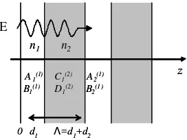
We used the combination of linear refractive indices of layer-1 and layer-2 are 1.8 and 1.6, respectively. The layer-1 is made from nonlinear optical material with nonlinear refractive index nnl =
2.2 x 10⁻⁵ cm2/GW. We calculated the transmittance of the structure using matrix transfer [Eqn. (17)] by varying light input intensity as shown in Fig. 2(a). The light intensity leads to the change of photonic bandgap position to the longer wavelength. If we take the constant wavelength at 1.555 µm, it is clear that its transmission increases ~ 70% with the increase of light intensity as shown in Fig. 2(b). This behaviour (change of transmittance from low to high with light intensity) is a characteristic of all- optical switching device.
1.550 1.555 1.56 1.565 0.2
0.4 0.6 0.8 1
λ [micrometer]
Transmittance
1 GW/cm2 5 GW/cm2 15 GW/cm2
(a)
0 5 10 15
0 0.2 0.4 0.6 0.8
Input intensity [GW/cm2]
Transmittance
(b)
In order to study the effect of the depth variation of refractive index caused by the combination of the change of nonlinear refractive index and the length of the structure (kL) on the switching behavior, we applied Eqn. (20) and the results are shown in Fig. 3. The behavior of its switching is called optical bistability. It is clear that optical bistability depends on the value of kL; it occurs on the large value of
kL. If the length of the structure is kept constant, the optical bistability occurs when the nonlinear refractive index is increased.
0 0.5 1 1.5 2 2.5 3 3.5
0 0.5 1 1.5 2 2.5
Input intensity [GW/cm2]
Output intensity [GW/cm
2]
κL = 1.0
κL = 2.0
κL = 3.24
Figure 3. Optical bistability for different value of kL
4.3. Photonic crystal with equal linear refractive index but opposite sign of nonlinear refractive index
In this structure, the refractive indices of each layers are n1 = 1.5 + 0.01 I and n2 = 1.5 – 0.01 I.
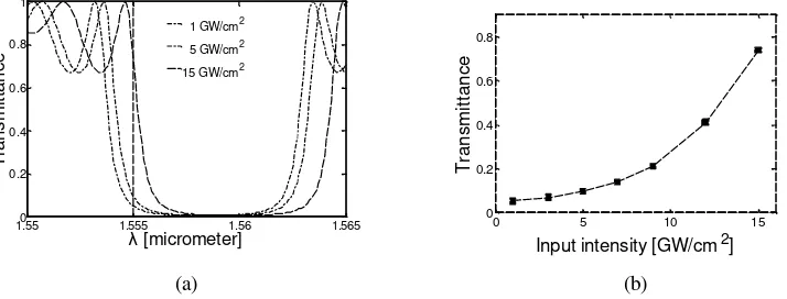
The thicknesses of the layers are given the values corresponding to a quarter wave structure for a wavelength of 1 µm and refractive index of n0 = 1.5 (d1 = d2 = 0.1667 µm). Transmittance of the
structure for various numbers of layers with very low input intensity (0.5 GW/cm2) is shown in Fig. 4. For low numbers of layers, no photonic bandgap is observed. The PBG get deeper and sharper with the increase numbers of layers due to the large numbers interaction of waves which are reflected and transmitted at each interface.
0.985 0.99 0.995 1 1.005 1.01 1.015
0 0.1 0.2 0.3 0.4 0.5 0.6 0.7 0.8 0.9 1
λ [micrometer]
Transmittance N = 10
N = 200
N = 600
Figure 4. Evolution of transmittance spectra of the structure with n0 = 1.5 and |nn l| = 0.01 cm 2
/GW for different numbers of layers. The input light intensity is 0.5 GW/cm2
.
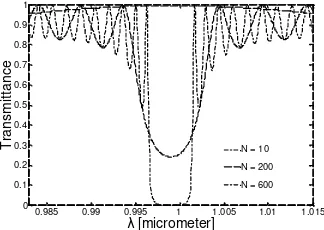
To study the potential of this structure for all-optical switching device, we plot in Fig. 5(a) the transmittance spectra of this structure with 200 layers for three different values of input intensities, i.e. 0.5 , 1.0 and 1.5 GW/cm2. The width and depth of the PBG are increased with the increase value of the input light intensity. The solid vertical line indicates the change of transmission at the wavelength of 0.995 µm with different input intensity. Its transmittance decreases allmost 100% (all-optical switching) when the input intensity is increased from 0.5 GW/cm2 to 1.5 GW/cm2, as shown in Fig. 5(b). This behaviour is caused by the increase of different of refractive index ∆n = n1 - n2. Therefore, the width of
0.980 0.99 1 1.01 1.02 0.2
0.4 0.6 0.8 1
λ [micrometer]
Transmittance 0.5 GW/cm2
1.0 GW/cm2
1.5 GW/cm2
(a)
0.4 0.6 0.8 1.0 1.2 1.4 1.6
0.0 0.2 0.4 0.6 0.8
1.0 λ = 0.995 µm
Transmittance
Input intensity [GW/cm2]
(b)
Figure 5. (a). Evolution of transmittance spectra of the structure with 200 layers for three different input intensity. (b). Transmission changes of the wavelength of 0.995 µm as the input intensity increases.
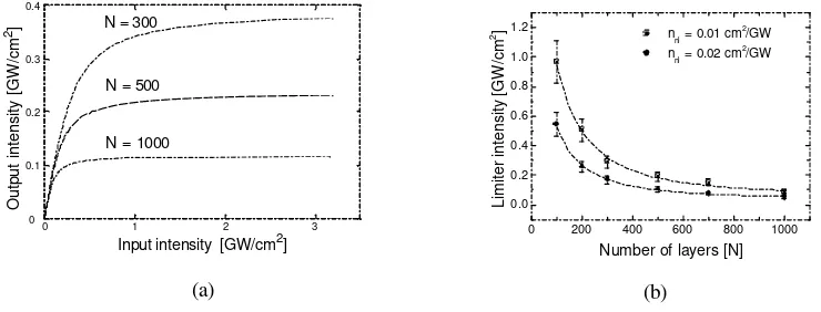
We also plot the relation between output and input light intensity in Fig. 6(a) for different values of number of layers. For very low incident intensity the transmitted intensity is equal to the incident intensity. As the input intensity is increased, the output intensity begins to saturate at the limiting value. This value is the most desired for optical limiter, i.e. a device to maintain the low output intensity for the large input intensity. The limiting value is then called as limiter intensity which is decreased with the increase numbers of layers and the increase of nonlinear refractive index value as shown in Fig. 6(b).
0 1 2 3
0 0.1 0.2 0.3 0.4
Input intensity [GW/cm2]
Output intensity [GW/cm
2] N = 300
N = 500
N = 1000
(a)
0 200 400 600 800 1000
0.0 0.2 0.4 0.6 0.8 1.0
1.2 n
nl = 0.01 cm 2
/GW nnl = 0.02 cm2
/GW
Limiter intensity [GW/cm
2]
Number of layers [N]
(b)
Figure 6. Output intensity as a function of input intensity for the structure (a) with numbers of layers 300, 500 and 100 layers, (b) with nonlinear refractive index of 0.01 cm2/GW and 0.02 cm2/GW.
V. CONCLUSION
We studied two structures of 1D nonlinear photonic crystals for all-optical switching and optical limiter devices, i.e. nonlinear Distributed Bragg Reflector (DBR) and nonlinear photonic crystal composed of nonlinear optical materials with identical linear refractive index but opposite sign of their nonlinear refractive index. We concluded that an appropriate combination of refractive indices of two materials, the position of PBG can be tuned. The first structure can be used for all- optical switching at the widely used telecommunication wavelength (1.55 µm) and the last once might be used both for all-optical switching and all-optical limiter devices. The limiter intensity is reduced with the increase of number of layers (N) and the magnitude of nonlinear refractive index of the layers (nnl).
ACKNOWLEDGEMENTS
REFERENCES
[1] G. I. Stegeman in “Nonlinear Optics of Organic Molecules and Polymers”, H. S. Nalwa and S. Miyata (Eds.), CRC Press Inc. 1997, 799.
[2] U. Gubler, “Third-Order Nonlinear Effects in Organic Materials”, PhD Dissertation, Zurich Swiss, 2000. [3] M. A. Bader, G. Marowsky, A. Bahtiar, K. Koynov, C. Bubeck, H. Tillmann, H. - H. Hörhold, S. Pereira, “
PPV-Derivatives: New Promising Materials for Nonlinear All-Optical Waveguide Switching”, J. Opt. Soc. Am. B 19
(2002), 2250.
[4] J. D. Joannopoulos, R. D. Meade, J. N. Winn, “Photonic Crystals; Molding the Flow of Light”, Princeton University Press, 1995.
[5] K. Sakoda, “Optical Properties of Photonic Crystals”, Springer Verlag Berlin, 2001. [6] P. Yeh, Optical wave in layered media, John Wiley & Son, New York, 1988.