PQFP/TQFP
2 3 1
I N D E X C O R N E R
3 4 P1.0 VCC
P1.1
P1.2
P1.4 P1.3 NC 4 2 4 3 4 14 0
6 5 4 4 4 3 2 2 6 2 5 2 8 2 7 2 4 1 81 92 02 12 2 P 1 . 7
P 1 . 6 P 1 . 5 N C 7 8 9 1 0 1 1
1 21 31 41 51 61 7
2 9 3 0 3 93 83 73 63 5
3 3 3 2 3 1
N C P S E N
XT AL1 GND XT AL2 GND P0.0 (AD0)
A L E / P R O G
()
P
3
.7
RD
E A / V P P
()
P
3
.6
WR
( R X D ) P 3 . 0
P 0 . 7 ( A D 7 )
P 2 . 6 ( A 1 4 ) P 0 . 6 ( A D 6 ) P 0 . 5 ( A D 5 ) P 0 . 4 ( A D 4 )
P0.3 (AD3) P0.2 (AD2) P0.1 (AD1)
(I N T 0) P 3 . 2 ( T X D ) P 3 . 1 ( T 1 ) P 3 . 5 (I N T 1) P 3 . 3 ( T 0 ) P 3 . 4
P 2 . 7 ( A 1 5 )
(A11) P2.3 (A12) P2.4 (A10) P2.2 (A 9) P 2 .1 (A 8) P 2 .0
R S T
P 2 . 5 ( A 1 3 )
• Fully Static Operation: 0 Hz to 24 MHz
• Three-Level Program Memory Lock
• 128 x 8-Bit Internal RAM
• 32 Programmable I/O Lines
• Two 16-Bit Timer/Counters
• Six Interrupt Sources
• Programmable Serial Channel
• Low Power Idle and Power Down Modes
Description
The AT89C51 is a low-power, high-performance CMOS 8-bit microcomputer with 4K bytes of Flash Programmable and Erasable Read Only Memory (PEROM). The device is manufactured using Atmel’s high density nonvolatile memory technology and is compatible with the industry standard MCS-51™ instruction set and pinout. The on-chip Flash allows the program memory to be reprogrammed in-system or by a con-ventional nonvolatile memory programmer. By combining a versatile 8-bit CPU with Flash on a monolithic chip, the Atmel AT89C51 is a powerful microcomputer which provides a highly flexible and cost effective solution to many embedded control appli-cations.
PDIP
P 1 . 0 VC C P 1 . 1 P 0 . 0 ( A D 0 )
P 1 . 2
(I N T 0) P 3 . 2
A L E / P R O G
(R D) P 3 . 7 P 2 . 3 ( A 1 1 ) ( T X D ) P 3 . 1
E A / V P P
(W R) P 3 . 6 P 2 . 4 ( A 1 2 ) ( R X D ) P 3 . 0
P 0 . 7 ( A D 7 )
( T 1 ) P 3 . 5
P 2 . 6 ( A 1 4 ) R S T
P 0 . 6 ( A D 6 )
P 1 . 7
P 0 . 5 ( A D 5 )
P 1 . 6
P 0 . 4 ( A D 4 )
P 1 . 5
P 0 . 3 ( A D 3 )
P 1 . 4
P 0 . 2 ( A D 2 )
P 1 . 3
P 0 . 1 ( A D 1 )
(I N T 1) P 3 . 3
P S E N
X TA L 2 P 2 . 2 ( A 1 0 ) ( T 0 ) P 3 . 4
P 2 . 7 ( A 1 5 )
X TA L 1 P 2 . 1 ( A 9 ) G N D P 2 . 0 ( A 8 ) P 2 . 5 ( A 1 3 )
2 0 1 9 1 8 1 7 1 6 1 5 1 2 3 4 5 6 7 8 9 1 0 1 1 1 2 1 3 1 4 2 1 2 2 2 3 2 4 2 5 2 6 4 0 3 9 3 8 3 7 3 6 3 5 3 4 3 3 3 2 3 1 3 0 2 9 2 8 2 7 0265F-A–12/97 (continued)
8-Bit
Microcontroller
with 4K Bytes
Flash
AT89C51
Pin Configurations
PLCC P1.0 VCC P1.1 P0.0 (AD0) P1.2A L E / P R O G
() P 3 . 7 RD XT AL1
E A / V P P
() P 3 . 6 WR GND
( R X D ) P 3 . 0
P 0 . 7 ( A D 7 )
P 2 . 6 ( A 1 4 ) P 0 . 6 ( A D 6 ) P 0 . 5 ( A D 5 ) P 0 . 4 ( A D 4 )
P0.3 (AD3) P1.4 P0.2 (AD2) P1.3 P0.1 (AD1)
P S E N
XT
AL2
(I N T 0) P 3 . 2 ( T X D ) P 3 . 1
( T 1 ) P 3 . 5 (I N T 1) P 3 . 3 ( T 0 ) P 3 . 4
P 2 . 7 ( A 1 5 )
(A11) P2.3 (A12) P2.4 (A10) P2.2 (A 9) P 2 .1 (A 8) P 2 .0 NC 2 3 1
R S T P 1 . 7 P 1 . 6 P 1 . 5 I N D E X C O R N E R
N C
NC
P 2 . 5 ( A 1 3 ) 3 4 N C 4 2 4 3 4 14 0 6
543 2 4 4
2 6 2 5
2 8 2 7 1 81 92 02 12 2 2 4 7 8 9 1 0 1 1 1 2 1 3 1 4 1 5 1 6
1 7 2 9
Block Diagram
PORT 2 DRIVERS
PORT 2 LATCH
P2.0 - P2.7
FLASH PORT 0
LATCH RAM
PROGRAM ADDRESS REGISTER
BUFFER
PC INCREMENTER
PROGRAM COUNTER
DPTR RAM ADDR.
REGISTER
INSTRUCTION REGISTER B
REGISTER
INTERRUPT, SERIAL PORT, AND TIMER BLOCKS
STACK POINTER ACC
TMP2 TMP1
ALU
PSW
TIMING AND CONTROL
PORT 3 LATCH
PORT 3 DRIVERS
P3.0 - P3.7 PORT 1
LATCH
PORT 1 DRIVERS
P1.0 - P1.7 OSC
GND VCC
PSEN
ALE/PROG EA / VPP
RST
The AT89C51 provides the following standard features: 4K bytes of Flash, 128 bytes of RAM, 32 I/O lines, two 16-bit timer/counters, a five vector two-level interrupt architecture, a full duplex serial port, on-chip oscillator and clock cir-cuitry. In addition, the AT89C51 is designed with static logic for operation down to zero frequency and supports two software selectable power saving modes. The Idle Mode stops the CPU while allowing the RAM, timer/counters, serial port and interrupt system to continue functioning. The Power Down Mode saves the RAM contents but freezes the oscillator disabling all other chip functions until the next hardware reset.
Pin Description
VCC Supply voltage. GND Ground. Port 0Port 0 is an 8-bit open drain bidirectional I/O port. As an output port each pin can sink eight TTL inputs. When 1s are written to port 0 pins, the pins can be used as high-impedance inputs.
Port 0 may also be configured to be the multiplexed low-order address/data bus during accesses to external pro-gram and data memory. In this mode P0 has internal pul-lups.
Port 0 also receives the code bytes during Flash program-ming, and outputs the code bytes during program tion. External pullups are required during program verifica-tion.
Port 1
Port 1 is an 8-bit bidirectional I/O port with internal pullups. The Port 1 output buffers can sink/source four TTL inputs. When 1s are written to Port 1 pins they are pulled high by the internal pullups and can be used as inputs. As inputs, Port 1 pins that are externally being pulled low will source current (IIL) because of the internal pullups.
Port 1 also receives the low-order address bytes during Flash programming and verification.
Port 2
Port 2 is an 8-bit bidirectional I/O port with internal pullups. The Port 2 output buffers can sink/source four TTL inputs. When 1s are written to Port 2 pins they are pulled high by the internal pullups and can be used as inputs. As inputs, Port 2 pins that are externally being pulled low will source current (IIL) because of the internal pullups.
Port 2 emits the high-order address byte during fetches from external program memory and during accesses to external data memory that use 16-bit addresses (MOVX @ DPTR). In this application it uses strong internal pullups
when emitting 1s. During accesses to external data mem-ory that use 8-bit addresses (MOVX @ RI), Port 2 emits the contents of the P2 Special Function Register.
Port 2 also receives the high-order address bits and some control signals during Flash programming and verification.
Port 3
Port 3 is an 8-bit bidirectional I/O port with internal pullups. The Port 3 output buffers can sink/source four TTL inputs. When 1s are written to Port 3 pins they are pulled high by the internal pullups and can be used as inputs. As inputs, Port 3 pins that are externally being pulled low will source current (IIL) because of the pullups.
Port 3 also serves the functions of various special features of the AT89C51 as listed below:
Port 3 also receives some control signals for Flash pro-gramming and verification.
RST
Reset input. A high on this pin for two machine cycles while the oscillator is running resets the device.
ALE/PROG
Address Latch Enable output pulse for latching the low byte of the address during accesses to external memory. This pin is also the program pulse input (PROG) during Flash programming.
In normal operation ALE is emitted at a constant rate of 1/6 the oscillator frequency, and may be used for external tim-ing or clocktim-ing purposes. Note, however, that one ALE pulse is skipped during each access to external Data Mem-ory.
If desired, ALE operation can be disabled by setting bit 0 of SFR location 8EH. With the bit set, ALE is active only dur-ing a MOVX or MOVC instruction. Otherwise, the pin is weakly pulled high. Setting the ALE-disable bit has no effect if the microcontroller is in external execution mode.
PSEN
Program Store Enable is the read strobe to external pro-gram memory.
Port Pin Alternate Functions
P3.0 RXD (serial input port) P3.1 TXD (serial output port) P3.2 INT0 (external interrupt 0) P3.3 INT1 (external interrupt 1) P3.4 T0 (timer 0 external input) P3.5 T1 (timer 1 external input)
When the AT89C51 is executing code from external pro-gram memory, PSEN is activated twice each machine cycle, except that two PSEN activations are skipped during each access to external data memory.
EA/VPP
External Access Enable. EA must be strapped to GND in order to enable the device to fetch code from external pro-gram memory locations starting at 0000H up to FFFFH. Note, however, that if lock bit 1 is programmed, EA will be internally latched on reset.
EA should be strapped to VCC for internal program execu-tions.
This pin also receives the 12-volt programming enable volt-age (VPP) during Flash programming, for parts that require 12-volt VPP.
XTAL1
Input to the inverting oscillator amplifier and input to the internal clock operating circuit.
XTAL2
Output from the inverting oscillator amplifier.
Oscillator Characteristics
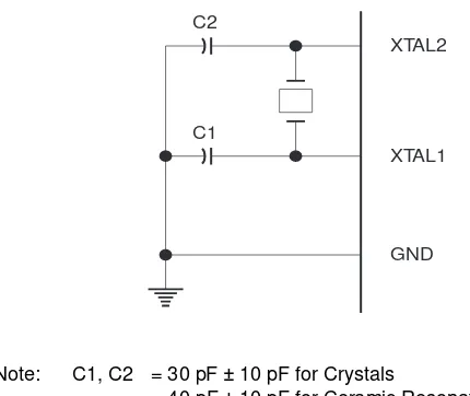
XTAL1 and XTAL2 are the input and output, respectively, of an inverting amplifier which can be configured for use as an on-chip oscillator, as shown in Figure 1. Either a quartz crystal or ceramic resonator may be used. To drive the device from an external clock source, XTAL2 should be left unconnected while XTAL1 is driven as shown in Figure 2. There are no requirements on the duty cycle of the external clock signal, since the input to the internal clocking circuitry is through a divide-by-two flip-flop, but minimum and maxi-mum voltage high and low time specifications must be observed.
Idle Mode
In idle mode, the CPU puts itself to sleep while all the on-chip peripherals remain active. The mode is invoked by software. The content of the on-chip RAM and all the spe-cial functions registers remain unchanged during this mode. The idle mode can be terminated by any enabled interrupt or by a hardware reset.
It should be noted that when idle is terminated by a hard ware reset, the device normally resumes program execu-tion, from where it left off, up to two machine cycles before the internal reset algorithm takes control. On-chip hardware inhibits access to internal RAM in this event, but access to the port pins is not inhibited. To eliminate the possibility of an unexpected write to a port pin when Idle is terminated by reset, the instruction following the one that invokes Idle should not be one that writes to a port pin or to external memory.
Figure 1. Oscillator Connections
Note: C1, C2 = 30 pF ± 10 pF for Crystals
= 40 pF ± 10 pF for Ceramic Resonators
Figure 2. External Clock Drive Configuration
C2
XTAL2
GND XTAL1 C1
Status of External Pins During Idle and Power Down Modes
Mode Program Memory ALE PSEN PORT0 PORT1 PORT2 PORT3
Power Down Mode
In the power down mode the oscillator is stopped, and the instruction that invokes power down is the last instruction executed. The on-chip RAM and Special Function Regis-ters retain their values until the power down mode is termi-nated. The only exit from power down is a hardware reset. Reset redefines the SFRs but does not change the on-chip RAM. The reset should not be activated before VCC is restored to its normal operating level and must be held active long enough to allow the oscillator to restart and sta-bilize.
Program Memory Lock Bits
On the chip are three lock bits which can be left unpro-grammed (U) or can be prounpro-grammed (P) to obtain the addi-tional features listed in the table below:
When lock bit 1 is programmed, the logic level at the EA pin is sampled and latched during reset. If the device is pow-ered up without a reset, the latch initializes to a random value, and holds that value until reset is activated. It is nec-essary that the latched value of EA be in agreement with the current logic level at that pin in order for the device to function properly.
Lock Bit Protection Modes
Program Lock Bits Protection Type
LB1 LB2 LB3
1 U U U No program lock features.
2 P U U MOVC instructions executed from external program memory are disabled from fetching code bytes from internal memory, EA is sampled and latched on reset, and further programming of the Flash is disabled.
3 P P U Same as mode 2, also verify is disabled.
4 P P P Same as mode 3, also external execution is disabled.
Programming the Flash
The AT89C51 is normally shipped with the on-chip Flash memory array in the erased state (that is, contents = FFH) and ready to be programmed. The programming interface accepts either a high-voltage (12-volt) or a low-voltage (VCC) program enable signal. The low voltage program-ming mode provides a convenient way to program the AT89C51 inside the user’s system, while the high-voltage programming mode is compatible with conventional third party Flash or EPROM programmers.
The AT89C51 is shipped with either the high-voltage or low-voltage programming mode enabled. The respective top-side marking and device signature codes are listed in the following table.
The AT89C51 code memory array is programmed byte-by-byte in either programming mode. To program any non-blank byte in the on-chip Flash Memory, the entire memory must be erased using the Chip Erase Mode.
Programming Algorithm: Before programming the AT89C51, the address, data and control signals should be set up according to the Flash programming mode table and Figures 3 and 4. To program the AT89C51, take the follow-ing steps.
1. Input the desired memory location on the address lines.
2. Input the appropriate data byte on the data lines. 3. Activate the correct combination of control signals. 4. Raise EA/VPP to 12V for the high-voltage programming
mode.
5. Pulse ALE/PROG once to program a byte in the Flash array or the lock bits. The byte-write cycle is self-timed and typically takes no more than 1.5 ms. Repeat steps 1 through 5, changing the address and data for the entire array or until the end of the object file is reached.
Data Polling: The AT89C51 features Data Polling to indi-cate the end of a write cycle. During a write cycle, an attempted read of the last byte written will result in the com-plement of the written datum on PO.7. Once the write cycle has been completed, true data are valid on all outputs, and the next cycle may begin. Data Polling may begin any time after a write cycle has been initiated.
Ready/Busy: The progress of byte programming can also be monitored by the RDY/BSY output signal. P3.4 is pulled low after ALE goes high during programming to indicate BUSY. P3.4 is pulled high again when programming is done to indicate READY.
VPP = 12V VPP = 5V
Program Verify: If lock bits LB1 and LB2 have not been programmed, the programmed code data can be read back via the address and data lines for verification. The lock bits cannot be verified directly. Verification of the lock bits is achieved by observing that their features are enabled.
Chip Erase: The entire Flash array is erased electrically by using the proper combination of control signals and by holding ALE/PROG low for 10 ms. The code array is written with all “1”s. The chip erase operation must be executed before the code memory can be re-programmed.
Reading the Signature Bytes: The signature bytes are read by the same procedure as a normal verification of locations 030H,
031H, and 032H, except that P3.6 and P3.7 must be pulled to a logic low. The values returned are as follows.
(030H) = 1EH indicates manufactured by Atmel (031H) = 51H indicates 89C51
(032H) = FFH indicates 12V programming (032H) = 05H indicates 5V programming
Programming Interface
Every code byte in the Flash array can be written and the entire array can be erased by using the appropriate combi-nation of control signals. The write operation cycle is self-timed and once initiated, will automatically time itself to completion.
All major programming vendors offer worldwide support for the Atmel microcontroller series. Please contact your local programming vendor for the appropriate software revision.
Flash Programming Modes
Note: 1. Chip Erase requires a 10-ms PROG pulse.
Mode RST PSEN ALE/PROG EA/VPP P2.6 P2.7 P3.6 P3.7
Write Code Data H L H/12V L H H H
Read Code Data H L H H L L H H
Write Lock Bit - 1 H L H/12V H H H H
Bit - 2 H L H/12V H H L L
Bit - 3 H L H/12V H L H L
Chip Erase H L H/12V H L L L
Read Signature Byte H L H H L L L L
Figure 3. Programming the Flash Figure 4. Verifying the Flash
P1
P2.6
P3.6 P2.0 - P2.3 A0 - A7
ADDR. OOOOH/OFFFH T SEE FLASH PROGRAMMING MODES ABLE 3-24 MHz
A8 - A11 P0
+5V
P2.7
PGM DATA
PROG
V /VIH PP
VIH ALE P3.7 XTAL2 EA RST PSEN XTAL1 GND VCC AT89C51 P1 P2.6 P3.6 P2.0 - P2.3 A0 - A7
ADDR. OOOOH/0FFFH
3-24 MHz
A8 - A11
P0 +5V P2.7 PGM DATA (USE 10K PULLUPS) VIH VIH ALE P3.7 XTAL2 EA RST PSEN XTAL1 GND VCC AT89C51 T SEE FLASH PROGRAMMING MODES ABLE
Flash Programming and Verification Characteristics
TA = 0°C to 70°C, VCC = 5.0 ± 10%
Note: 1. Only used in 12-volt programming mode.
Symbol Parameter Min Max Units
VPP(1) Programming Enable Voltage 11.5 12.5 V
IPP(1) Programming Enable Current 1.0 mA
1/tCLCL Oscillator Frequency 3 24 MHz
tAVGL Address Setup to PROG Low 48tCLCL
tGHAX Address Hold After PROG 48tCLCL
tDVGL Data Setup to PROG Low 48tCLCL
tGHDX Data Hold After PROG 48tCLCL
tEHSH P2.7 (ENABLE) High to VPP 48tCLCL
tSHGL VPP Setup to PROG Low 10 µs
tGHSL(1) VPP Hold After PROG 10 µs
tGLGH PROG Width 1 110 µs
tAVQV Address to Data Valid 48tCLCL
tELQV ENABLE Low to Data Valid 48tCLCL
tEHQZ Data Float After ENABLE 0 48tCLCL
tGHBL PROG High to BUSY Low 1.0 µs
Flash Programming and Verification Waveforms - High Voltage Mode (V
PP
= 12V)
tGLGH tGHSL
tAVGL
tSHGL
tDVGL
tGHAX
tAVQV
tGHDX
tEHSH
tELQV
tWC
BUSY READY
tGHBL
tEHQZ P1.0 - P1.7
P2.0 - P2.3
ALE/PROG PORT 0
LOGIC 1 LOGIC 0
EA/VPP
VPP
P2.7 (ENABLE)
P3.4 (RDY/BSY)
PROGRAMMING ADDRESS
VERIFICATION ADDRESS
DATA IN DATA OUT
Flash Programming and Verification Waveforms - Low Voltage Mode (V
PP
= 5V)
tGLGH tAVGL
tSHGL
tDVGL
tGHAX
tAVQV
tGHDX
tEHSH
tELQV
tWC
BUSY READY
tGHBL
tEHQZ P1.0 - P1.7
P2.0 - P2.3
ALE/PROG PORT 0
LOGIC 1 LOGIC 0
EA/VPP
P2.7 (ENABLE)
P3.4 (RDY/BSY)
PROGRAMMING ADDRESS
VERIFICATION ADDRESS
Absolute Maximum Ratings*
DC Characteristics
TA = -40°C to 85°C, VCC = 5.0V ± 20% (unless otherwise noted)
Notes: 1. Under steady state (non-transient) conditions, IOL must be externally limited as follows: Maximum IOL per port pin: 10 mA
Maximum IOL per 8-bit port: Port 0: 26 mA Ports 1, 2, 3: 15 mA Maximum total IOL for all output pins: 71 mA
If IOL exceeds the test condition, VOL may exceed the related specification. Pins are not guaranteed to sink current greater
than the listed test conditions. 2. Minimum VCC for Power Down is 2V.
Operating Temperature ... -55°C to +125°C *NOTICE: Stresses beyond those listed under “Absolute Maximum Ratings” may cause permanent dam-age to the device. This is a stress rating only and functional operation of the device at these or any other conditions beyond those indicated in the operational sections of this specification is not implied. Exposure to absolute maximum rating conditions for extended periods may affect device reliability.
Storage Temperature ... -65°C to +150°C Voltage on Any Pin
with Respect to Ground ...-1.0V to +7.0V Maximum Operating Voltage... 6.6V DC Output Current... 15.0 mA
Symbol Parameter Condition Min Max Units
VIL Input Low Voltage (Except EA) -0.5 0.2 VCC - 0.1 V
VIL1 Input Low Voltage (EA) -0.5 0.2 VCC - 0.3 V
VIH Input High Voltage (Except XTAL1, RST) 0.2 VCC + 0.9 VCC + 0.5 V
VIH1 Input High Voltage (XTAL1, RST) 0.7 VCC VCC + 0.5 V
VOL Output Low Voltage(1) (Ports 1,2,3) IOL = 1.6 mA 0.45 V
VOL1 Output Low Voltage(1) (Port 0, ALE, PSEN)
IOL = 3.2 mA 0.45 V
VOH Output High Voltage (Ports 1,2,3, ALE, PSEN)
IOH = -60 µA, VCC = 5V ± 10% 2.4 V
IOH = -25 µA 0.75 VCC V
IOH = -10 µA 0.9 VCC V
VOH1 Output High Voltage
(Port 0 in External Bus Mode)
IOH = -800 µA, VCC = 5V ± 10% 2.4 V
IOH = -300 µA 0.75 VCC V
IOH = -80 µA 0.9 VCC V
IIL Logical 0 Input Current (Ports 1,2,3) VIN = 0.45V -50 µA
ITL Logical 1 to 0 Transition Current (Ports 1,2,3)
VIN = 2V, VCC = 5V ± 10% -650 µA
ILI Input Leakage Current (Port 0, EA) 0.45 < VIN < VCC ±10 µA
RRST Reset Pulldown Resistor 50 300 KΩ
CIO Pin Capacitance Test Freq. = 1 MHz, TA = 25°C 10 pF
ICC Power Supply Current Active Mode, 12 MHz 20 mA
Idle Mode, 12 MHz 5 mA
Power Down Mode(2) VCC = 6V 100 µA
AC Characteristics
(Under Operating Conditions; Load Capacitance for Port 0, ALE/PROG, and PSEN = 100 pF; Load Capacitance for all other outputs = 80 pF)
External Program and Data Memory Characteristics
Symbol Parameter 12 MHz Oscillator 16 to 24 MHz Oscillator Units
Min Max Min Max
1/tCLCL Oscillator Frequency 0 24 MHz
tLHLL ALE Pulse Width 127 2tCLCL-40 ns
tAVLL Address Valid to ALE Low 43 tCLCL-13 ns
tLLAX Address Hold After ALE Low 48 tCLCL-20 ns
tLLIV ALE Low to Valid Instruction In 233 4tCLCL-65 ns
tLLPL ALE Low to PSEN Low 43 tCLCL-13 ns
tPLPH PSEN Pulse Width 205 3tCLCL-20 ns
tPLIV PSEN Low to Valid Instruction In 145 3tCLCL-45 ns
tPXIX Input Instruction Hold After PSEN 0 0 ns
tPXIZ Input Instruction Float After PSEN 59 tCLCL-10 ns
tPXAV PSEN to Address Valid 75 tCLCL-8 ns
tAVIV Address to Valid Instruction In 312 5tCLCL-55 ns
tPLAZ PSEN Low to Address Float 10 10 ns
tRLRH RD Pulse Width 400 6tCLCL-100 ns
tWLWH WR Pulse Width 400 6tCLCL-100 ns
tRLDV RD Low to Valid Data In 252 5tCLCL-90 ns
tRHDX Data Hold After RD 0 0 ns
tRHDZ Data Float After RD 97 2tCLCL-28 ns
tLLDV ALE Low to Valid Data In 517 8tCLCL-150 ns
tAVDV Address to Valid Data In 585 9tCLCL-165 ns
tLLWL ALE Low to RD or WR Low 200 300 3tCLCL-50 3tCLCL+50 ns
tAVWL Address to RD or WR Low 203 4tCLCL-75 ns
tQVWX Data Valid to WR Transition 23 tCLCL-20 ns
tQVWH Data Valid to WR High 433 7tCLCL-120 ns
tWHQX Data Hold After WR 33 tCLCL-20 ns
tRLAZ RD Low to Address Float 0 0 ns
External Program Memory Read Cycle
External Data Memory Read Cycle
tLHLL
tLLIV
tPLIV
tLLAX tPXIZ
tPLPH
tPLAZ tPXAV
tAVLL
tLLPL
tAVIV
tPXIX ALE
PSEN
PORT 0
PORT 2 A8 - A15
A0 - A7 A0 - A7 A8 - A15 INSTR IN
tLHLL
tLLDV
tLLWL
tLLAX
tWHLH
tAVLL
tRLRH
tAVDV
tAVWL
tRLAZ t
RHDX
tRLDV tRHDZ
A0 - A7 FROM RI OR DPL
ALE
PSEN
RD
PORT 0
PORT 2 P2.0 - P2.7 OR A8 - A15 FROM DPH
A0 - A7 FROM PCL
External Data Memory Write Cycle
External Clock Drive Waveforms
External Clock Drive
Symbol Parameter Min Max Units
1/tCLCL Oscillator Frequency 0 24 MHz
tCLCL Clock Period 41.6 ns
tCHCX High Time 15 ns
tCLCX Low Time 15 ns
tCLCH Rise Time 20 ns
tCHCL Fall Time 20 ns
tLHLL
tLLWL
tLLAX
tWHLH
tAVLL
tWLWH
tAVWL
tQVWX
tQVWH
tWHQX
A0 - A7 FROM RI OR DPL
ALE
PSEN
WR
PORT 0
PORT 2 P2.0 - P2.7 OR A8 - A15 FROM DPH
A0 - A7 FROM PCL
A8 - A15 FROM PCH DATA OUT INSTR IN
tCHCX tCHCX
tCLCX
tCLCL
tCHCL tCLCH
V - 0.5VCC
0.45V
Serial Port Timing: Shift Register Mode Test Conditions
(VCC = 5.0 V ± 20%; Load Capacitance = 80 pF)
Shift Register Mode Timing Waveforms
Symbol Parameter 12 MHz Osc Variable Oscillator Units
Min Max Min Max
tXLXL Serial Port Clock Cycle Time 1.0 12tCLCL µs
tQVXH Output Data Setup to Clock Rising Edge 700 10tCLCL-133 ns
tXHQX Output Data Hold After Clock Rising Edge 50 2tCLCL-117 ns
tXHDX Input Data Hold After Clock Rising Edge 0 0 ns
tXHDV Clock Rising Edge to Input Data Valid 700 10tCLCL-133 ns
tXHDV
tQVXH
tXLXL
tXHDX tXHQX
ALE
INPUT DATA CLEAR RI OUTPUT DATA
WRITE TO SBUF
INSTRUCTION CLOCK
0
0 1
1 2
2 3
3 4
4 5
5 6
6 7
7 SET TI SET RI
8
VALID VALID VALID VALID VALID VALID VALID VALID
Float Waveforms
(1)
Note: 1. For timing purposes, a port pin is no longer floating when a 100 mV change from load voltage occurs. A port pin begins to float when 100 mV change from the loaded VOH/VOL level occurs.
VLOAD+ 0.1V
Timing Reference Points V
LOAD- 0.1V LOAD
V VOL+ 0.1V
VOL- 0.1V
AC Testing Input/Output Waveforms
(1)
Note: 1. AC Inputs during testing are driven at VCC - 0.5V for
a logic 1 and 0.45V for a logic 0. Timing measure-ments are made at VIH min. for a logic 1 and VIL
max. for a logic 0.
0.45V
TEST POINTS V - 0.5VCC
0.2 V + 0.9VCC
Ordering Information
Speed (MHz)
Power
Supply Ordering Code Package Operation Range
12 5V ± 20% AT89C51-12AC 44A Commercial
AT89C51-12JC 44J (0°C to 70°C)
AT89C51-12PC 40P6
AT89C51-12QC 44Q
AT89C51-12AI 44A Industrial
AT89C51-12JI 44J (-40°C to 85°C)
AT89C51-12PI 40P6
AT89C51-12QI 44Q
AT89C51-12AA 44A Automotive
AT89C51-12JA 44J (-40°C to 105°C)
AT89C51-12PA 40P6
AT89C51-12QA 44Q
16 5V ± 20% AT89C51-16AC 44A Commercial
AT89C51-16JC 44J (0°C to 70°C)
AT89C51-16PC 40P6
AT89C51-16QC 44Q
AT89C51-16AI 44A Industrial
AT89C51-16JI 44J (-40°C to 85°C)
AT89C51-16PI 40P6
AT89C51-16QI 44Q
AT89C51-16AA 44A Automotive
AT89C51-16JA 44J (-40°C to 105°C)
AT89C51-16PA 40P6
AT89C51-16QA 44Q
20 5V ± 20% AT89C51-20AC 44A Commercial
AT89C51-20JC 44J (0°C to 70°C)
AT89C51-20PC 40P6
AT89C51-20QC 44Q
AT89C51-20AI 44A Industrial
AT89C51-20JI 44J (-40°C to 85°C)
AT89C51-20PI 40P6
Ordering Information
Speed (MHz)
Power
Supply Ordering Code Package Operation Range
24 5V ± 20% AT89C51-24AC 44A Commercial
AT89C51-24JC 44J (0°C to 70°C)
AT89C51-24PC 44P6
AT89C51-24QC 44Q
AT89C51-24AI 44A Industrial
AT89C51-24JI 44J (-40°C to 85°C)
AT89C51-24PI 44P6
AT89C51-24QI 44Q
Package Type
44A 44 Lead, Thin Plastic Gull Wing Quad Flatpack (TQFP)
44J 44 Lead, Plastic J-Leaded Chip Carrier (PLCC)
40P6 40 Lead, 0.600” Wide, Plastic Dual Inline Package (PDIP)
EVERLIGHT ELECTRONICS CO., LTD.
Device Number: DMO-851-005 REV:
1.1
MODEL NO:
IRM-8510/N
ECN:
Page: 1/9
MODEL NO:
IRM-8510/N
ECN:
Page: 2/9
■
NOTES
:
1. This drawing measure is a standard value. All dimensions are in millimeter.
2. In case of designation is tolerance
±
0.3mm.
3. Lead spacing is measured where the lead emerge from the package.
4. Above specification may be changed without notice. EVERLIGHT will reserve authority
on material change for above specification.
5. These specification sheets include materials protected under copyright of EVERLIGHT
corporation. Please don't reproduce or cause anyone to reproduce them without
EVERLIGHT consent.
EVERLIGHT ELECTRONICS CO., LTD.
Device Number: DMO-851-005 REV:
1.1
MODEL NO:
IRM-8510/N
ECN:
Page: 3/9
■
Description
:
1. The module is a small type infrared remote control system receiver which has been
developed and designed by utilizing the latest hybrid technology.
2. This single unit type module incorporates a photo diode and a receiving preamplifier IC.
3. The demodulated output signal can directly be decoded by a microprocessor.
■
Feature
:
1.
High protection ability to EMI and metal case can be customized.
2.
Mold type and metal case type to meet the design of front panel.
3.
Elliptic lens to improve the characteristic against
4.
Line-up for various center carrier frequencies.
5.
Low voltage and low power consumption.
6.
High immunity against ambient light.
7.
Photodiode with integrated circuit.
8.
TTL and CMOS compatibility.
9.
Long reception distance.
10.
High sensitivity.
■
Application
:
1.
Optical switch
2.
Light detecting portion of remote control
•
AV instruments such as Audio, TV, VCR, CD, MD, etc.
•
Home appliances such as Air-conditioner, Fan , etc.
•
The other equipments with wireless remote control.
•
CATV set top boxes
MODEL NO:
IRM-8510/N
ECN:
Page: 4/9
■
Absolute maximum ratings
:
(Ta=25
℃
)
Parameter
Symbol
Ratings
Unit
Notice
Supply Voltage
Vcc
4.3~5.7
V
Operating Temperature
Topr
-10
〜
+60
℃
Storage Temperature
Tstg
-20
〜
+70
℃
Soldering Temperature
Tsol
260
℃
4mm from mold body
less than 5 seconds
■
Electro Optical Characteristics
:
(Ta=25
℃
)
Parameter
Symbol
MIN
TYP
MAX
Unit
Condition
Supply Voltage
Vcc
4.7
5
5.3
V
DC voltage
Supply Current
Icc
-
-
3
mA
No signal input
B.P.F Center
Frequency
fo
-
37.9
-
KHz
Peak Wavelength
λ
p
-
940
-
nm
L
05
-
-Transmission
Distance
L
452.5
-
m
At the ray axis
*1
Half Angle
θ
-
45
-
deg
High Level Pulse
Width
T
H400
-
800
µ
s
Low Level Pulse
Width
T
L400
-
800
µ
s
At the ray axis
*2
High Level Output
Voltage
V
H4.5
-
-
V
Low Level Output
Voltage
V
L0.5
V
*1:The ray receiving surface at a vertex and relation to the ray axis in the
range of
φ
= 0
°
and
φ
=45
°
.
EVERLIGHT ELECTRONICS CO., LTD.
Device Number: DMO-851-005 REV:
1.1
MODEL NO:
IRM-8510/N
ECN:
Page: 5/9
■
TEST METHOD
:
The specified electro-optical characteristics is satisfied under the following
Conditions at the controllable distance.
c
Measurement place
A place that is nothing of extreme light reflected in the room.
d
External light
Project the light of ordinary white fluorescent lamps which are not high
Frequency lamps and must be less then 10 Lux at the module surface.
(Ee
≦
10Lux)
e
Standard transmitter
A transmitter whose output is so adjusted as to
Vo=400mVp-p and the output
Wave form shown in Fig.-1.According to the measurement method shown in
Fig.-2 the standard transmitter is specified. However, the infrared photodiode
to be used for the transmitter should be
λ
p=940nm,
∆λ
=50nm. Also, photo
diode is used of PD438B (V
R=5V).
(Standard light / Light source temperature 2856
°
K).
f
Measuring system
Carrier frequency is adjusted to center frequency of each product.
IR TANSMITTER OUTPUT WAVE FORM
OUTPUT PULSE OF DEVICE
θ
θ
D.U.T
L: Transmission Distance
Standard Transmitter
GND
Vcc
OUT
Vout
Standard Transmitter
Oscilloscope Vout 10uF
+5.0± 0.1V 10k
20cm
10
0k
8
ABLC AMP
B.P.F. + TRAP
4
DEMODURATION
WAVE FORM ARRANGEMENT
3
22K OHM 47 OHM
5
7
6
2
1
130K OHM 47uF
+
-Vcc
LIMITER IN +
-IN
C1
GND CD
C2 10nF
OUT fo
R2 Vcc
OUT
GND PD438B
Pre-AMP
MODEL NO:
IRM-8510/N
ECN:
Page: 6/9
■
Module schematic & circuit
:
Fig.-1 Transmitter Wave Form
D.U.T Output Pulse
Fig.-2 Measuring Method
Fig.-3 Measuring System
θ
EVERLIGHT ELECTRONICS CO., LTD.
Device Number: DMO-851-005 REV:
1.1
MODEL NO:
IRM-8510/N
ECN:
Page: 7/9
■
TYPICAL ELECTRICAL/OPTICAL/CHARACTERISTICS CURVES
Fig.-4 Relative Spectral Sensitivity vs. Wavelength
Fig.-5 Relative Transmission Distance vs. Direction
Fig.-6 Output Pulse Length vs. Arrival Distance
Fig.-7 Arrival Distance vs. Supply Voltage
Fig.-8 Relative Transmission Distance
vs. Center Carrier Frequency
Fig.-9 Arrival Distance
MODEL NO:
IRM-8510/N
ECN:
Page: 8/9
■
Reliability test item and condition
:
The reliability of products shall be satisfied with items listed below.
Confidence level: 90%
LTPD: 10%
Samples(n)
Test Items
Test Conditions
Failure Judgement
Criteria
Defective(c)
Operation life
Vcc=5V,Ta:25
℃
1000hrs
n=22,c=0
Temperature
cycle
1 cycle -20
℃
+25
℃
+70
℃
(30min) 5min (30min)
50 cycle test
n=22,c=0
Thermal shock
-10
℃
to +70
℃
(5min) (10sec) (5min)
50 cycle test
L
0≦
L
×
0.8
L
45≦
L
×
0.8
n=22,c=0
High temperature
storage
Temp: +70
℃
1000hrs
n=22,c=0
Low temperature
storage
Temp: -20
℃
1000hrs
n=22,c=0
High temperature
High humidity
Ta: 85
℃
RH:85% 1000hrs
n=22,c=0
Solder heat
Temp: 260
±
5
℃
5sec
4mm Form the bottom of the
package.
L: Lower
specification limit
n=22,c=0
Solderability
Temp: 230
±
5
℃
5sec
4mm Form the bottom of the
package.
More than 90% of
Lead to be covered
by soldering
R L
Label
UNIT:cm
E V E
2.Box
15
3.Carton
2.0
21
1.Plastic Case
22
I G H T
Label
Opto-electronic,Compoments EVERLIGHT
9
14.5
33
24
48
EVERLIGHT ELECTRONICS CO., LTD.
Device Number: DMO-851-005 REV:
1.1
MODEL NO:
IRM-8510/N
ECN:
Page: 9/9
■
■
■
■
Packing Specifications
CPN
:
Customer’s Production Number
P/N
:
Production Number
QTY
:
Packing Quantity
CAT
:
Ranks
HUE
:
Peak Wavelength
REF :
Reference
LOT NO : Lot Number
MADE IN TAIWAN
:
Production place
mov
a,#00h
mov
r0,#8
mov
r1,#0
mov
p1,#00h
mov
tmod,#21h
start:
jb
p2.1,$
acall
delay2
acall
delay
mulai:
jb
p2.1,tambah
ljmp
tetep
two:
jb
p2.1,tambah1
ljmp
tetep1
three:
jb
p2.1,tambah2
ljmp
tetep2
four:
jb
p2.1,tambah3
ljmp
tetep3
five:
jb
p2.1,tambah4
ljmp
tetep4
tambah:
inc
r1
nop
nop
nop
ljmp
two
tetep:
nop
nop
nop
ljmp
two
tambah1:
inc
r1
nop
nop
nop
ljmp
three
nop
nop
nop
ljmp
three
tambah2:
inc
r1
nop
nop
nop
ljmp
four
tetep2:
nop
nop
nop
ljmp
four
tambah3:
inc
r1
nop
nop
nop
ljmp
five
tetep3:
nop
nop
nop
ljmp
five
tambah4:
inc
r1
nop
nop
nop
ljmp
poiu
tetep4:
nop
nop
nop
ljmp
poiu
poiu:
cjne
r1,#05,satu
sjmp
nol
djnz
r0,mulai
aaa:
mov
p0,a
cjne
a,#01h,cex
ljmp
awal1
cex:
cjne
a,#02h,cex1
ljmp
awal1
cex1:
cjne
a,#02h,kirim_ulang
ljmp
awal1
kirim_ulang:
mov
r2,#20
ool:
setb
p1.0
nop
nop
nop
nop
nop
nop
nop
nop
nop
nop
nop
clr
p1.0
nop
nop
nop
nop
nop
nop
nop
nop
nop
nop
nop
djnz
r1,ool
ljmp
start
mov
a,#00h
mov
r0,#8
mov
r1,#0
mov
p1,#00h
mov
tmod,#21h
start1:
jb
p2.1,$
acall
delay2
acall
delay
mulai1:
jb
p2.1,tambah0
ljmp
tetep0
two1:
jb
p2.1,tambah11
ljmp
tetep11
three1:
jb
p2.1,tambah21
ljmp
tetep21
four1:
jb
p2.1,tambah31
ljmp
tetep31
five1:
jb
p2.1,tambah41
ljmp
tetep41
tambah0:
inc
r1
nop
nop
nop
ljmp
two1
tetep0:
nop
nop
nop
ljmp
two1
tambah11:
inc
r1
nop
nop
nop
ljmp
three1
nop
nop
ljmp
four1
tetep21:
nop
nop
nop
ljmp
four1
tambah31:
inc
r1
nop
nop
nop
ljmp
five1
tetep31:
nop
nop
nop
ljmp
five1
tambah41:
inc
r1
nop
nop
nop
ljmp
poiu1
tetep41:
nop
nop
nop
ljmp
poiu1
poiu1:
cjne
r1,#05,satu1
sjmp
nol1
satu1:
setb
acc.0
rr
A
djnz
r0,mulai1
sjmp
aaa1
nol1:
clr
acc.0
rr
A
djnz
r0,mulai1
mov
p0,a
cjne
a,#0fah,kirim_ulang1
ljmp
awal1
kirim_ulang1:
mov
r2,#20
ool1:
setb
p1.0
nop
nop
nop
nop
nop
nop
nop
nop
nop
nop
nop
clr
p1.0
nop
nop
nop
nop
nop
nop
nop
nop
nop
nop
nop
djnz
r1,ool1
ljmp
start1
awal00:
mov
a,#00h
mov
r0,#8
mov
r1,#0
mov
p1,#00h
mov
tmod,#21h
start00:
ljmp
tetep100
three00:
jb
p2.1,tambah200
ljmp
tetep200
four00:
jb
p2.1,tambah300
ljmp
tetep300
five00:
jb
p2.1,tambah400
ljmp
tetep400
tambah00:
inc
r1
nop
nop
nop
ljmp
two00
tetep00:
nop
nop
nop
ljmp
two00
tambah100:
inc
r1
nop
nop
nop
ljmp
three00
tetep100:
nop
nop
nop
ljmp
three00
tambah200:
inc
r1
nop
nop
nop
ljmp
four00
tetep200:
nop
nop
nop
tambah300:
inc
r1
nop
nop
nop
ljmp
five00
tetep300:
nop
nop
nop
ljmp
five00
tambah400:
inc
r1
nop
nop
nop
ljmp
poiu00
tetep400:
nop
nop
nop
ljmp
poiu00
poiu00:
cjne
r1,#05,satu00
sjmp
nol00
satu00:
setb
acc.0
rr
A
djnz
r0,mulai00
sjmp
aaa00
nol00:
clr
acc.0
rr
A
djnz
r0,mulai00
aaa00:
mov
p0,a
cjne
a,#00h,kirim_ulang00
ljmp
awal00
kirim_ulang00:
mov
r2,#20
ool00:
nop
nop
nop
nop
clr
p1.0
nop
nop
nop
nop
nop
nop
nop
nop
nop
nop
nop
djnz
r1,ool00
ljmp
start00
kirim_serial:
mov
th1,#0f3h
mov
tl1,#0f3h
setb
tr1
mov
r1,#01h
mov
r2,#55h
mov
r3,#00h
mov
a,r1
mov
sbuf,a
jnb
ti,$
clr
ti
mov
a,r2
mov
sbuf,a
jnb
ti,$
clr
ti
mov
a,r3
mov
sbuf,a
jnb
ti,$
clr
ti
sjmp
selesai
delay:
mov
tl0,#0ffh
setb
tr0
jnb
tf0,$
clr
tr0
clr
tf0
ret
delay2:
mov
th0,#00h
mov
tl0,#00h
setb
tr0
jnb
tf0,$
clr
tr0
clr
tf0
ret
selesai:
ljmp
start
org
000bh
cpl
p1.0
reti
start:
mov
a,#00000001b
setb
p1.0
acall
delay
mov
R0,#9
setb
et0
mov
tmod,#12h
mov
th0,#0f0h
mov
tl0,#0f0h
setb
ea
haha:
mov
th1,#00h
mov
tl1,#00h
setb
tr1
setb
tr0
jnb
tf1,$
clr
tr0
clr
tr1
clr
tf1
rl
A
banding:
djnz
r0,jalan
sjmp
start
jalan:
rr
A
jb
Acc.0,satu
sjmp
nol
nol:
mov
th1,#00h
mov
tl1,#00h
setb
tr1
setb
tr0
jnb
tf1,$
clr
tr0
clr
tr1
sjmp
banding
satu:
clr
p1.0
mov
th1,#00h
mov
tl1,#00h
setb
tr1
jnb
tf1,$
clr
tr1
clr
tf1
sjmp
banding
cek_bit:
mov
th1,#00h
mov
tl1,#00h
setb
tr1
cek:
jb
p2.1,kk
clr
tf1
clr
tr1
sjmp
start
kk:
jnb
tf1,cek
clr
tf1
clr
tr1
start1:
mov
a,#11111010b
setb
p1.0
acall
delay
mov
R0,#9
setb
et0
mov
tmod,#12h
mov
th0,#0f0h
mov
tl0,#0f0h
setb
ea
haha1:
mov
th1,#00h
mov
tl1,#00h
setb
tr1
setb
tr0
jnb
tf1,$
jalan1:
rr
A
jb
Acc.0,satu1
sjmp
nol1
nol1:
mov
th1,#00h
mov
tl1,#00h
setb
tr1
setb
tr0
jnb
tf1,$
clr
tr0
clr
tr1
clr
tf1
sjmp
banding1
satu1:
clr
p1.0
mov
th1,#00h
mov
tl1,#00h
setb
tr1
jnb
tf1,$
clr
tr1
clr
tf1
sjmp
banding1
cek_bit1:
mov
th1,#00h
mov
tl1,#00h
setb
tr1
cek1:
jb
p2.1,kk1
clr
tf1
clr
tr1
sjmp
start1
kk1:
jnb
tf1,cek1
clr
tf1
clr
tr1
start2:
mov
a,#00000000b
setb
p1.0
acall
delay
setb
et0
mov
tmod,#12h
mov
th0,#0f0h
mov
tl0,#0f0h
setb
ea
haha2:
mov
th1,#00h
mov
tl1,#00h
setb
tr1
setb
tr0
jnb
tf1,$
clr
tr0
clr
tr1
clr
tf1
rl
A
banding2:
djnz
r0,jalan2
sjmp
start2
jalan2:
rr
A
jb
Acc.0,satu2
sjmp
nol2
nol2:
mov
th1,#00h
mov
tl1,#00h
setb
tr1
setb
tr0
jnb
tf1,$
clr
tr0
clr
tr1
clr
tf1
sjmp
banding2
satu2:
clr
p1.0
mov
th1,#00h
mov
tl1,#00h
setb
tr1
jnb
tf1,$
clr
tr1
clr
tf1
clr
tf1
clr
tr1
sjmp
start2
kk2:
jnb
tf1,cek2
clr
tf1
clr
tr1
sjmp
selesai
delay:
mov
r7,#8
loop:
mov
r6,#250
loop2:
mov
r5,#250
loop3:
djnz
r5,$
djnz
r6,loop2
djnz
r7,loop
ret
selesai: