1
• 4K Bytes of In-System Programmable (ISP) Flash Memory – Endurance: 1000 Write/Erase Cycles
• 4.0V to 5.5V Operating Range
• Fully Static Operation: 0 Hz to 33 MHz • Three-level Program Memory Lock • 128 x 8-bit Internal RAM
• 32 Programmable I/O Lines • Two 16-bit Timer/Counters • Six Interrupt Sources
• Full Duplex UART Serial Channel • Low-power Idle and Power-down Modes • Interrupt Recovery from Power-down Mode • Watchdog Timer
• Dual Data Pointer • Power-off Flag
• Fast Programming Time
• Flexible ISP Programming (Byte and Page Mode)
Description
The AT89S51 is a low-power, high-performance CMOS 8-bit microcontroller with 4K bytes of in-system programmable Flash memory. The device is manufactured using Atmel’s high-density nonvolatile memory technology and is compatible with the indus-try-standard 80C51 instruction set and pinout. The on-chip Flash allows the program memory to be reprogrammed in-system or by a conventional nonvolatile memory pro-grammer. By combining a versatile 8-bit CPU with in-system programmable Flash on a monolithic chip, the Atmel AT89S51 is a powerful microcontroller which provides a highly-flexible and cost-effective solution to many embedded control applications. The AT89S51 provides the following standard features: 4K bytes of Flash, 128 bytes of RAM, 32 I/O lines, Watchdog timer, two data pointers, two 16-bit timer/counters, a five-vector two-level interrupt architecture, a full duplex serial port, on-chip oscillator, and clock circuitry. In addition, the AT89S51 is designed with static logic for operation down to zero frequency and supports two software selectable power saving modes. The Idle Mode stops the CPU while allowing the RAM, timer/counters, serial port, and interrupt system to continue functioning. The Power-down mode saves the RAM con-tents but freezes the oscillator, disabling all other chip functions until the next external interrupt or hardware reset.
8-bit
Microcontroller
with 4K Bytes
In-System
Programmable
Flash
AT89S51
Pin Configurations
XTAL2 XTAL1 GND GND
3
Pin Description
VCC Supply voltage.
GND Ground.
Port 0 Port 0 is an 8-bit open drain bidirectional I/O port. As an output port, each pin can sink eight TTL inputs. When 1s are written to port 0 pins, the pins can be used as high-impedance inputs.
Port 0 can also be configured to be the multiplexed low-order address/data bus during accesses to external program and data memory. In this mode, P0 has internal pull-ups. Port 0 also receives the code bytes during Flash programming and outputs the code bytes during program verification. External pull-ups are required during program verification.
Port 1 Port 1 is an 8-bit bidirectional I/O port with internal pull-ups. The Port 1 output buffers can sink/source four TTL inputs. When 1s are written to Port 1 pins, they are pulled high by the internal pull-ups and can be used as inputs. As inputs, Port 1 pins that are externally being pulled low will source current (IIL) because of the internal pull-ups.
Port 1 also receives the low-order address bytes during Flash programming and verification.
Port 2 Port 2 is an 8-bit bidirectional I/O port with internal pull-ups. The Port 2 output buffers can sink/source four TTL inputs. When 1s are written to Port 2 pins, they are pulled high by the internal pull-ups and can be used as inputs. As inputs, Port 2 pins that are externally being pulled low will source current (IIL) because of the internal pull-ups.
Port 2 emits the high-order address byte during fetches from external program memory and during accesses to external data memory that use 16-bit addresses (MOVX @ DPTR). In this application, Port 2 uses strong internal pull-ups when emitting 1s. During accesses to external data memory that use 8-bit addresses (MOVX @ RI), Port 2 emits the contents of the P2 Spe-cial Function Register.
Port 2 also receives the high-order address bits and some control signals during Flash pro-gramming and verification.
Port 3 Port 3 is an 8-bit bidirectional I/O port with internal pull-ups. The Port 3 output buffers can sink/source four TTL inputs. When 1s are written to Port 3 pins, they are pulled high by the internal pull-ups and can be used as inputs. As inputs, Port 3 pins that are externally being pulled low will source current (IIL) because of the pull-ups.
Port 3 receives some control signals for Flash programming and verification.
Port 3 also serves the functions of various special features of the AT89S51, as shown in the following table.
Port Pin Alternate Functions
5
2487A–10/01
RST Reset input. A high on this pin for two machine cycles while the oscillator is running resets the device. This pin drives High for 98 oscillator periods after the Watchdog times out. The DIS-RTO bit in SFR AUXR (address 8EH) can be used to disable this feature. In the default state of bit DISRTO, the RESET HIGH out feature is enabled.
ALE/PROG Address Latch Enable (ALE) is an output pulse for latching the low byte of the address during accesses to external memory. This pin is also the program pulse input (PROG) during Flash programming.
In normal operation, ALE is emitted at a constant rate of 1/6 the oscillator frequency and may be used for external timing or clocking purposes. Note, however, that one ALE pulse is skipped during each access to external data memory.
If desired, ALE operation can be disabled by setting bit 0 of SFR location 8EH. With the bit set, ALE is active only during a MOVX or MOVC instruction. Otherwise, the pin is weakly pulled high. Setting the ALE-disable bit has no effect if the microcontroller is in external execution mode.
PSEN Program Store Enable (PSEN) is the read strobe to external program memory.
When the AT89S51 is executing code from external program memory, PSEN is activated twice each machine cycle, except that two PSEN activations are skipped during each access to external data memory.
EA/VPP External Access Enable. EA must be strapped to GND in order to enable the device to fetch code from external program memory locations starting at 0000H up to FFFFH. Note, however, that if lock bit 1 is programmed, EA will be internally latched on reset.
EA should be strapped to VCC for internal program executions.
This pin also receives the 12-volt programming enable voltage (VPP) during Flash programming.
XTAL1 Input to the inverting oscillator amplifier and input to the internal clock operating circuit.
XTAL2 Output from the inverting oscillator amplifier
Port Pin Alternate Functions
P3.0 RXD (serial input port) P3.1 TXD (serial output port) P3.2 INT0 (external interrupt 0) P3.3 INT1 (external interrupt 1) P3.4 T0 (timer 0 external input) P3.5 T1 (timer 1 external input)
Special
Function
Registers
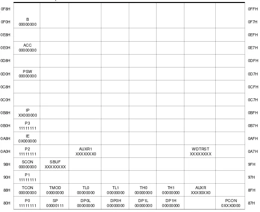
A map of the on-chip memory area called the Special Function Register (SFR) space is shown in Table 1.
Note that not all of the addresses are occupied, and unoccupied addresses may not be imple-mented on the chip. Read accesses to these addresses will in general return random data, and write accesses will have an indeterminate effect.
Table 1. AT89S51 SFR Map and Reset Values
7
2487A–10/01
User software should not write 1s to these unlisted locations, since they may be used in future products to invoke new features. In that case, the reset or inactive values of the new bits will always be 0.
Interrupt Registers: The individual interrupt enable bits are in the IE register. Two priorities can be set for each of the five interrupt sources in the IP register.
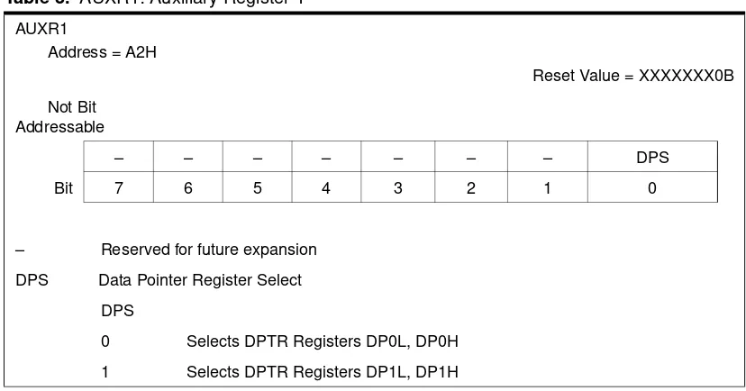
Dual Data Pointer Registers: To facilitate accessing both internal and external data memory, two banks of 16-bit Data Pointer Registers are provided: DP0 at SFR address locations 82H-83H and DP1 at 84H-85H. Bit DPS = 0 in SFR AUXR1 selects DP0 and DPS = 1 selects DP1. The user should always initialize the DPS bit to the appropriate value before accessing the respective Data Pointer Register.
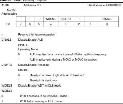
Table 2. AUXR: Auxiliary Register
AUXR Address = 8EH Reset Value = XXX00XX0B
Not Bit Addressable
– – – WDIDLE DISRTO – – DISALE
Bit 7 6 5 4 3 2 1 0
– Reserved for future expansion DISALE Disable/Enable ALE
DISALE Operating Mode
0 ALE is emitted at a constant rate of 1/6 the oscillator frequency 1 ALE is active only during a MOVX or MOVC instruction DISRTO Disable/Enable Reset out
DISRTO
0 Reset pin is driven High after WDT times out 1 Reset pin is input only
WDIDLE Disable/Enable WDT in IDLE mode WDIDLE
Power Off Flag: The Power Off Flag (POF) is located at bit 4 (PCON.4) in the PCON SFR. POF is set to “1” during power up. It can be set and rest under software control and is not affected by reset.
Memory
Organization
MCS-51 devices have a separate address space for Program and Data Memory. Up to 64K bytes each of external Program and Data Memory can be addressed.
Program Memory If the EA pin is connected to GND, all program fetches are directed to external memory. On the AT89S51, if EA is connected to VCC, program fetches to addresses 0000H through FFFH are directed to internal memory and fetches to addresses 1000H through FFFFH are directed to external memory.
Data Memory The AT89S51 implements 128 bytes of on-chip RAM. The 128 bytes are accessible via direct and indirect addressing modes. Stack operations are examples of indirect addressing, so the 128 bytes of data RAM are available as stack space.
Watchdog
Timer
(One-time
Enabled with
Reset-out)
The WDT is intended as a recovery method in situations where the CPU may be subjected to software upsets. The WDT consists of a 14-bit counter and the Watchdog Timer Reset (WDTRST) SFR. The WDT is defaulted to disable from exiting reset. To enable the WDT, a user must write 01EH and 0E1H in sequence to the WDTRST register (SFR location 0A6H). When the WDT is enabled, it will increment every machine cycle while the oscillator is running. The WDT timeout period is dependent on the external clock frequency. There is no way to dis-able the WDT except through reset (either hardware reset or WDT overflow reset). When WDT overflows, it will drive an output RESET HIGH pulse at the RST pin.
Using the WDT
To enable the WDT, a user must write 01EH and 0E1H in sequence to the WDTRST register (SFR location 0A6H). When the WDT is enabled, the user needs to service it by writing 01EH and 0E1H to WDTRST to avoid a WDT overflow. The 14-bit counter overflows when it reaches 16383 (3FFFH), and this will reset the device. When the WDT is enabled, it will increment every machine cycle while the oscillator is running. This means the user must reset the WDTTable 3. AUXR1: Auxiliary Register 1 AUXR1
Address = A2H
Reset Value = XXXXXXX0B Not Bit
Addressable
– – – – – – – DPS
Bit 7 6 5 4 3 2 1 0
– Reserved for future expansion DPS Data Pointer Register Select
DPS
9
2487A–10/01
should be serviced in those sections of code that will periodically be executed within the time required to prevent a WDT reset.
WDT During
Power-down
and Idle
In down mode the oscillator stops, which means the WDT also stops. While in Power-down mode, the user does not need to service the WDT. There are two methods of exiting Power-down mode: by a hardware reset or via a level-activated external interrupt, which is enabled prior to entering Power-down mode. When Power-down is exited with hardware reset, servicing the WDT should occur as it normally does whenever the AT89S51 is reset. Exiting Power-down with an interrupt is significantly different. The interrupt is held low long enough for the oscillator to stabilize. When the interrupt is brought high, the interrupt is serviced. To pre-vent the WDT from resetting the device while the interrupt pin is held low, the WDT is not started until the interrupt is pulled high. It is suggested that the WDT be reset during the inter-rupt service for the interinter-rupt used to exit Power-down mode.
To ensure that the WDT does not overflow within a few states of exiting Power-down, it is best to reset the WDT just before entering Power-down mode.
Before going into the IDLE mode, the WDIDLE bit in SFR AUXR is used to determine whether the WDT continues to count if enabled. The WDT keeps counting during IDLE (WDIDLE bit = 0) as the default state. To prevent the WDT from resetting the AT89S51 while in IDLE mode, the user should always set up a timer that will periodically exit IDLE, service the WDT, and reenter IDLE mode.
With WDIDLE bit enabled, the WDT will stop to count in IDLE mode and resumes the count upon exit from IDLE.
UART
The UART in the AT89S51 operates the same way as the UART in the AT89C51. For further information on the UART operation, refer to the ATMEL Web site (http://www.atmel.com). From the home page, select ‘Products’, then ‘8051-Architecture Flash Microcontroller’, then ‘Product Overview’.Timer 0 and 1
Timer 0 and Timer 1 in the AT89S51 operate the same way as Timer 0 and Timer 1 in the AT89C51. For further information on the timers’ operation, refer to the ATMEL Web site (http://www.atmel.com). From the home page, select ‘Products’, then ‘8051-Architecture Flash Microcontroller’, then ‘Product Overview’.Interrupts
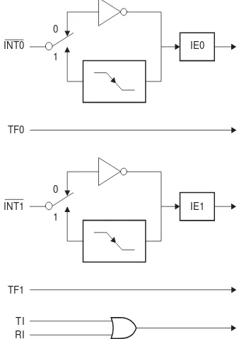
The AT89S51 has a total of five interrupt vectors: two external interrupts (INT0 and INT1), two timer interrupts (Timers 0 and 1), and the serial port interrupt. These interrupts are all shown in Figure 1.Each of these interrupt sources can be individually enabled or disabled by setting or clearing a bit in Special Function Register IE. IE also contains a global disable bit, EA, which disables all interrupts at once.
Note that Table 4 shows that bit position IE.6 is unimplemented. In the AT89S51, bit position IE.5 is also unimplemented. User software should not write 1s to these bit positions, since they may be used in future AT89 products.
.
Figure 1. Interrupt Sources
Table 4. Interrupt Enable (IE) Register
(MSB) (LSB)
EA – – ES ET1 EX1 ET0 EX0
Enable Bit = 1 enables the interrupt. Enable Bit = 0 disables the interrupt.
Symbol Position Function
EA IE.7 Disables all interrupts. If EA = 0, no interrupt is acknowledged. If EA = 1, each interrupt source is individually enabled or disabled by setting or clearing its enable bit.
– IE.6 Reserved
– IE.5 Reserved
ES IE.4 Serial Port interrupt enable bit
ET1 IE.3 Timer 1 interrupt enable bit
EX1 IE.2 External interrupt 1 enable bit
ET0 IE.1 Timer 0 interrupt enable bit
EX0 IE.0 External interrupt 0 enable bit
User software should never write 1s to reserved bits, because they may be used in future AT89 products.
IE1 IE0
1 1
0 0
TF1 TF0
INT1 INT0
11
2487A–10/01
Oscillator
Characteristics
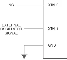
XTAL1 and XTAL2 are the input and output, respectively, of an inverting amplifier that can be configured for use as an on-chip oscillator, as shown in Figure 2. Either a quartz crystal or ceramic resonator may be used. To drive the device from an external clock source, XTAL2 should be left unconnected while XTAL1 is driven, as shown in Figure 3. There are no require-ments on the duty cycle of the external clock signal, since the input to the internal clocking circuitry is through a divide-by-two flip-flop, but minimum and maximum voltage high and low time specifications must be observed.
Figure 2. Oscillator Connections
Note: C1, C2 = 30 pF ± 10 pF for Crystals = 40 pF ± 10 pF for Ceramic Resonators
Figure 3. External Clock Drive Configuration
Idle Mode
In idle mode, the CPU puts itself to sleep while all the on-chip peripherals remain active. The mode is invoked by software. The content of the on-chip RAM and all the special function registers remain unchanged during this mode. The idle mode can be terminated by any enabled interrupt or by a hardware reset.Note that when idle mode is terminated by a hardware reset, the device normally resumes pro-gram execution from where it left off, up to two machine cycles before the internal reset algorithm takes control. On-chip hardware inhibits access to internal RAM in this event, but access to the port pins is not inhibited. To eliminate the possibility of an unexpected write to a port pin when idle mode is terminated by a reset, the instruction following the one that invokes idle mode should not write to a port pin or to external memory.
Power-down
Mode
In the down mode, the oscillator is stopped, and the instruction that invokes Power-down is the last instruction executed. The on-chip RAM and Special Function Registers retain their values until the Power-down mode is terminated. Exit from Power-down mode can be ini-tiated either by a hardware reset or by activation of an enabled external interrupt into INT0 or INT1. Reset redefines the SFRs but does not change the on-chip RAM. The reset should not be activated before VCC is restored to its normal operating level and must be held active long enough to allow the oscillator to restart and stabilize.
C2
XTAL2
GND XTAL1 C1
XTAL2
XTAL1
GND NC
EXTERNAL OSCILLATOR
Program
Memory Lock
Bits
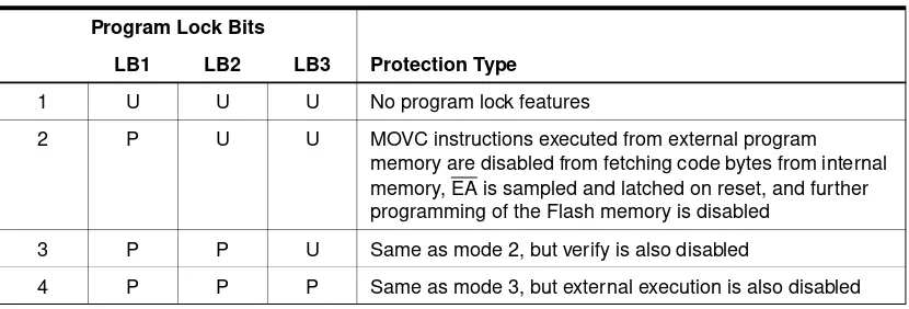
The AT89S51 has three lock bits that can be left unprogrammed (U) or can be programmed (P) to obtain the additional features listed in the following table.
When lock bit 1 is programmed, the logic level at the EA pin is sampled and latched during reset. If the device is powered up without a reset, the latch initializes to a random value and holds that value until reset is activated. The latched value of EA must agree with the current logic level at that pin in order for the device to function properly.
Programming
the Flash –
Parallel Mode
The AT89S51 is shipped with the on-chip Flash memory array ready to be programmed. The programming interface needs a high-voltage (12-volt) program enable signal and is compati-ble with conventional third-party Flash or EPROM programmers.
The AT89S51 code memory array is programmed byte-by-byte.
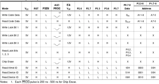
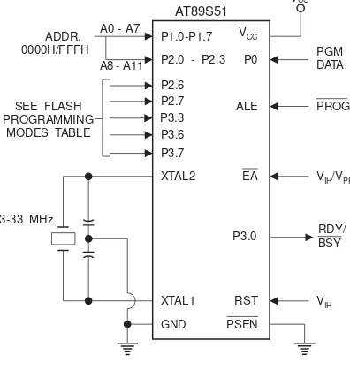
Programming Algorithm: Before programming the AT89S51, the address, data, and control signals should be set up according to the Flash programming mode table and Figures 13 and 14. To program the AT89S51, take the following steps:
1. Input the desired memory location on the address lines. 2. Input the appropriate data byte on the data lines. 3. Activate the correct combination of control signals. 4. Raise EA/VPP to 12V.
5. Pulse ALE/PROG once to program a byte in the Flash array or the lock bits. The byte-write cycle is self-timed and typically takes no more than 50 µs. Repeat steps 1 through 5, changing the address and data for the entire array or until the end of the object file is reached.
Data Polling: The AT89S51 features Data Polling to indicate the end of a byte write cycle. During a write cycle, an attempted read of the last byte written will result in the complement of the written data on P0.7. Once the write cycle has been completed, true data is valid on all
out-Table 5. Status of External Pins During Idle and Power-down Modes
Mode Program Memory ALE PSEN PORT0 PORT1 PORT2 PORT3
Idle Internal 1 1 Data Data Data Data
Idle External 1 1 Float Data Address Data
Power-down Internal 0 0 Data Data Data Data
Power-down External 0 0 Float Data Data Data
Table 6. Lock Bit Protection Modes Program Lock Bits
LB1 LB2 LB3 Protection Type
1 U U U No program lock features
2 P U U MOVC instructions executed from external program memory are disabled from fetching code bytes from internal memory, EA is sampled and latched on reset, and further programming of the Flash memory is disabled
3 P P U Same as mode 2, but verify is also disabled
13
2487A–10/01
Ready/Busy: The progress of byte programming can also be monitored by the RDY/BSY out-put signal. P3.0 is pulled low after ALE goes high during programming to indicate BUSY. P3.0 is pulled high again when programming is done to indicate READY.
Program Verify: If lock bits LB1 and LB2 have not been programmed, the programmed code data can be read back via the address and data lines for verification. The status of the individ-ual lock bits can be verified directly by reading them back.
Reading the Signature Bytes: The signature bytes are read by the same procedure as a nor-mal verification of locations 000H, 100H, and 200H, except that P3.6 and P3.7 must be pulled to a logic low. The values returned are as follows.
(000H) = 1EH indicates manufactured by Atmel (100H) = 51H indicates 89S51
(200H) = 06H
Chip Erase: In the parallel programming mode, a chip erase operation is initiated by using the proper combination of control signals and by pulsing ALE/PROG low for a duration of 200 ns -500 ns.
In the serial programming mode, a chip erase operation is initiated by issuing the Chip Erase instruction. In this mode, chip erase is self-timed and takes about 500 ms.
During chip erase, a serial read from any address location will return 00H at the data output.
Programming
the Flash –
Serial Mode
The Code memory array can be programmed using the serial ISP interface while RST is pulled to VCC. The serial interface consists of pins SCK, MOSI (input) and MISO (output). After
RST is set high, the Programming Enable instruction needs to be executed first before other operations can be executed. Before a reprogramming sequence can occur, a Chip Erase operation is required.
The Chip Erase operation turns the content of every memory location in the Code array into FFH.
Either an external system clock can be supplied at pin XTAL1 or a crystal needs to be con-nected across pins XTAL1 and XTAL2. The maximum serial clock (SCK) frequency should be less than 1/16 of the crystal frequency. With a 33 MHz oscillator clock, the maximum SCK fre-quency is 2 MHz.
Serial
Programming Algorithm
To program and verify the AT89S51 in the serial programming mode, the following sequence is recommended:
1. Power-up sequence:
Apply power between VCC and GND pins. Set RST pin to “H”.
If a crystal is not connected across pins XTAL1 and XTAL2, apply a 3 MHz to 33 MHz clock to XTAL1 pin and wait for at least 10 milliseconds.
2. Enable serial programming by sending the Programming Enable serial instruction to pin MOSI/P1.5. The frequency of the shift clock supplied at pin SCK/P1.7 needs to be less than the CPU clock at XTAL1 divided by 16.
3. The Code array is programmed one byte at a time in either the Byte or Page mode. The write cycle is self-timed and typically takes less than 0.5 ms at 5V.
4. Any memory location can be verified by using the Read instruction that returns the con-tent at the selected address at serial output MISO/P1.6.
Power-off sequence (if needed):
Set XTAL1 to “L” (if a crystal is not used). Set RST to “L”.
Turn VCC power off.
Data Polling: The Data Polling feature is also available in the serial mode. In this mode, dur-ing a write cycle an attempted read of the last byte written will result in the complement of the MSB of the serial output byte on MISO.
Serial
Programming Instruction Set
The Instruction Set for Serial Programming follows a 4-byte protocol and is shown in Table 8 on page 18.
Programming
Interface –
Parallel Mode
Every code byte in the Flash array can be programmed by using the appropriate combination of control signals. The write operation cycle is self-timed and once initiated, will automatically time itself to completion.
All major programming vendors offer worldwide support for the Atmel microcontroller series. Please contact your local programming vendor for the appropriate software revision.
Notes: 1. Each PROG pulse is 200 ns - 500 ns for Chip Erase. 2. Each PROG pulse is 200 ns - 500 ns for Write Code Data. 3. Each PROG pulse is 200 ns - 500 ns for Write Lock Bits. 4. RDY/BSY signal is output on P3.0 during programming. 5. X = don’t care.
Table 7. Flash Programming Modes
15
2487A–10/01
Figure 4. Programming the Flash Memory (Parallel Mode)
Figure 5. Verifying the Flash Memory (Parallel Mode)
Figure 6. Flash Programming and Verification Waveforms – Parallel Mode
Flash Programming and Verification Characteristics (Parallel Mode)
TA = 20°C to 30°C, VCC = 4.5 to 5.5VSymbol Parameter Min Max Units
VPP Programming Supply Voltage 11.5 12.5 V
IPP Programming Supply Current 10 mA
ICC VCC Supply Current 30 mA
1/tCLCL Oscillator Frequency 3 33 MHz
tAVGL Address Setup to PROG Low 48tCLCL
tGHAX Address Hold After PROG 48tCLCL
tDVGL Data Setup to PROG Low 48tCLCL
tGHDX Data Hold After PROG 48tCLCL
tEHSH P2.7 (ENABLE) High to VPP 48tCLCL
tSHGL VPP Setup to PROG Low 10 µs
tGHSL VPP Hold After PROG 10 µs
tGLGH PROG Width 0.2 1 µs
tAVQV Address to Data Valid 48tCLCL
tELQV ENABLE Low to Data Valid 48tCLCL
tEHQZ Data Float After ENABLE 0 48tCLCL
tGHBL PROG High to BUSY Low 1.0 µs
tWC Byte Write Cycle Time 50 µs
tGLGH tGHSL
tAVGL
tSHGL
tDVGL
tGHAX
tAVQV
tGHDX
tEHSH
tELQV
tWC
BUSY READY
tGHBL
tEHQZ P1.0 - P1.7
P2.0 - P2.3
ALE/PROG PORT 0
LOGIC 1 LOGIC 0
EA/VPP
VPP
P2.7 (ENABLE)
P3.0 (RDY/BSY)
PROGRAMMING ADDRESS
VERIFICATION ADDRESS
17
2487A–10/01
Figure 7. Flash Memory Serial Downloading
Flash Programming and Verification Waveforms – Serial Mode
Figure 8. Serial Programming Waveforms
P1.7/SCK DATA OUTPUT
INSTRUCTION INPUT
CLOCK IN
3-33 MHz
P1.5/MOSI
VIH
XTAL2
RST XTAL1
GND
VCC
AT89S51
P1.6/MISO
VCC
Notes: 1. The signature bytes are not readable in Lock Bit Modes 3 and 4. 2. B1 = 0, B2 = 0 → Mode 1, no lock protection
B1 = 0, B2 = 1 → Mode 2, lock bit 1 activated B1 = 1, B2 = 0 → Mode 3, lock bit 2 activated B1 = 1, B1 = 1 → Mode 4, lock bit 3 activated
After Reset signal is high, SCK should be low for at least 64 system clocks before it goes high to clock in the enable data bytes. No pulsing of Reset signal is necessary. SCK should be no faster than 1/16 of the system clock at XTAL1.
For Page Read/Write, the data always starts from byte 0 to 255. After the command byte and upper address byte are latched, each byte thereafter is treated as data until all 256 bytes are shifted in/out. Then the next instruction will be ready to be decoded.
Table 8. Serial Programming Instruction Set
Instruction
Instruction Format
Operation
Byte 1 Byte 2 Byte 3 Byte 4
Programming Enable 1010 1100 0101 0011 xxxx xxxx xxxx xxxx 0110 1001 (Output)
Enable Serial Programming while RST is high
Chip Erase 1010 1100 100x xxxx xxxx xxxx xxxx xxxx Chip Erase Flash memory array
Read Program Memory (Byte Mode)
0010 0000 xxxx Read data from Program
memory in the byte mode Write Program Memory
(Byte Mode)
0100 0000 xxxx Write data to Program
memory in the byte mode Write Lock Bits(2) 1010 1100 1110 00 xxxx xxxx xxxx xxxx Write Lock bits. See Note (2). Read Lock Bits 0010 0100 xxxx xxxx xxxx xxxx xx xx Read back current status of
the lock bits (a programmed lock bit reads back as a “1”) Read Signature Bytes(1) 0010 1000 xxx xxx xxxx Signature Byte Read Signature Byte
Read Program Memory (Page Mode)
0011 0000 xxxx Byte 0 Byte 1...
Byte 255
Read data from Program memory in the Page Mode (256 bytes)
Write Program Memory (Page Mode)
0101 0000 xxxx Byte 0 Byte 1...
Byte 255
Write data to Program memory in the Page Mode (256 bytes)
}
Each of the lock bits needs to be activated sequentially before Mode 4 can be executed.19
2487A–10/01
Serial Programming Characteristics
Figure 9. Serial Programming Timing
MOSI
MISO SCK
tOVSH
tSHSL
tSLSH
tSHOX
tSLIV
Table 9. Serial Programming Characteristics, TA = -40°C to 85°C, VCC = 4.0 - 5.5V (Unless Otherwise Noted)
Symbol Parameter Min Typ Max Units
1/tCLCL Oscillator Frequency 0 33 MHz
tCLCL Oscillator Period 30 ns
tSHSL SCK Pulse Width High 8 tCLCL ns
tSLSH SCK Pulse Width Low 8 tCLCL ns
tOVSH MOSI Setup to SCK High tCLCL ns
tSHOX MOSI Hold after SCK High 2 tCLCL ns
tSLIV SCK Low to MISO Valid 10 16 32 ns
tERASE Chip Erase Instruction Cycle Time 500 ms
Notes: 1. Under steady state (non-transient) conditions, IOL must be externally limited as follows: Maximum IOL per port pin: 10 mA
Maximum IOL per 8-bit port:
Port 0: 26 mA Ports 1, 2, 3: 15 mA Maximum total IOL for all output pins: 71 mA
Absolute Maximum Ratings*
Operating Temperature... -55°C to +125°C *NOTICE: Stresses beyond those listed under “Absolute Maximum Ratings” may cause permanent dam-age to the device. This is a stress rating only and functional operation of the device at these or any other conditions beyond those indicated in the operational sections of this specification is not implied. Exposure to absolute maximum rating conditions for extended periods may affect device reliability.
Storage Temperature ... -65°C to +150°C
Voltage on Any Pin
with Respect to Ground ...-1.0V to +7.0V
Maximum Operating Voltage ... 6.6V
DC Output Current... 15.0 mA
DC Characteristics
The values shown in this table are valid for TA = -40°C to 85°C and VCC = 4.0V to 5.5V, unless otherwise noted.
Symbol Parameter Condition Min Max Units
VIL Input Low Voltage (Except EA) -0.5 0.2 VCC-0.1 V
VIL1 Input Low Voltage (EA) -0.5 0.2 VCC-0.3 V
VIH Input High Voltage (Except XTAL1, RST) 0.2 VCC+0.9 VCC+0.5 V
VIH1 Input High Voltage (XTAL1, RST) 0.7 VCC VCC+0.5 V
VOL
Output Low Voltage(1) (Ports
1,2,3) IOL = 1.6 mA
0.45 V
VOL1
Output Low Voltage(1)
(Port 0, ALE, PSEN) IOL = 3.2 mA
0.45 V
VOH
Output High Voltage (Ports 1,2,3, ALE, PSEN)
IOH = -60 µA, VCC = 5V ± 10% 2.4 V
IOH = -25 µA 0.75 VCC V
IOH = -10 µA 0.9 VCC V
VOH1
Output High Voltage
(Port 0 in External Bus Mode)
IOH = -800 µA, VCC = 5V ± 10% 2.4 V
IOH = -300 µA 0.75 VCC V
IOH = -80 µA 0.9 VCC V
IIL
Logical 0 Input Current (Ports
1,2,3) VIN = 0.45V
-50 µA
ITL
Logical 1 to 0 Transition Current
(Ports 1,2,3) VIN = 2V, VCC = 5V ± 10%
-650 µA
ILI
Input Leakage Current (Port 0,
EA) 0.45 < VIN < VCC
±10 µA
RRST Reset Pulldown Resistor 50 300 KΩ
CIO Pin Capacitance Test Freq. = 1 MHz, TA = 25°C 10 pF
ICC
Power Supply Current
Active Mode, 12 MHz 25 mA
Idle Mode, 12 MHz 6.5 mA
21
2487A–10/01
AC Characteristics
Under operating conditions, load capacitance for Port 0, ALE/PROG, and PSEN = 100 pF; load capacitance for all other outputs = 80 pF.
External Program and Data Memory Characteristics
Symbol Parameter
12 MHz Oscillator Variable Oscillator
Units
Min Max Min Max
1/tCLCL Oscillator Frequency 0 33 MHz
tLHLL ALE Pulse Width 127 2tCLCL-40 ns
tAVLL Address Valid to ALE Low 43 tCLCL-25 ns
tLLAX Address Hold After ALE Low 48 tCLCL-25 ns
tLLIV ALE Low to Valid Instruction In 233 4tCLCL-65 ns
tLLPL ALE Low to PSEN Low 43 tCLCL-25 ns
tPLPH PSEN Pulse Width 205 3tCLCL-45 ns
tPLIV PSEN Low to Valid Instruction In 145 3tCLCL-60 ns
tPXIX Input Instruction Hold After PSEN 0 0 ns
tPXIZ Input Instruction Float After PSEN 59 tCLCL-25 ns
tPXAV PSEN to Address Valid 75 tCLCL-8 ns
tAVIV Address to Valid Instruction In 312 5tCLCL-80 ns
tPLAZ PSEN Low to Address Float 10 10 ns
tRLRH RD Pulse Width 400 6tCLCL-100 ns
tWLWH WR Pulse Width 400 6tCLCL-100 ns
tRLDV RD Low to Valid Data In 252 5tCLCL-90 ns
tRHDX Data Hold After RD 0 0 ns
tRHDZ Data Float After RD 97 2tCLCL-28 ns
tLLDV ALE Low to Valid Data In 517 8tCLCL-150 ns
tAVDV Address to Valid Data In 585 9tCLCL-165 ns
tLLWL ALE Low to RD or WR Low 200 300 3tCLCL-50 3tCLCL+50 ns
tAVWL Address to RD or WR Low 203 4tCLCL-75 ns
tQVWX Data Valid to WR Transition 23 tCLCL-30 ns
tQVWH Data Valid to WR High 433 7tCLCL-130 ns
tWHQX Data Hold After WR 33 tCLCL-25 ns
tRLAZ RD Low to Address Float 0 0 ns
External Program Memory Read Cycle
External Data Memory Read Cycle
tLHLL
tLLIV
tPLIV
tLLAX tPXIZ
tPLPH
tPLAZ
tPXAV tAVLL
tLLPL
tAVIV
tPXIX
ALE
PSEN
PORT 0
PORT 2 A8 - A15
A0 - A7 A0 - A7
A8 - A15 INSTR IN
tLHLL
tLLDV
tLLWL
tLLAX
tWHLH
tAVLL
tRLRH
tAVDV
tAVWL
tRLAZ
tRHDX
tRLDV tRHDZ
A0 - A7 FROM RI OR DPL ALE
PSEN
RD
PORT 0
PORT 2 P2.0 - P2.7 OR A8 - A15 FROM DPH
A0 - A7 FROM PCL
A8 - A15 FROM PCH
23
2487A–10/01
External Data Memory Write Cycle
External Clock Drive Waveforms
tLHLL
tLLWL
tLLAX
tWHLH
tAVLL
tWLWH
tAVWL tQVWX
tQVWH
tWHQX
A0 - A7 FROM RI OR DPL ALE
PSEN
WR
PORT 0
PORT 2 P2.0 - P2.7 OR A8 - A15 FROM DPH
A0 - A7 FROM PCL
A8 - A15 FROM PCH
DATA OUT INSTR IN
tCHCX tCHCX
tCLCX
tCLCL
tCHCL tCLCH
V - 0.5VCC
0.45V
0.2 VCC- 0.1V 0.7 VCC
External Clock Drive
Symbol Parameter Min Max Units
1/tCLCL Oscillator Frequency 0 33 MHz
tCLCL Clock Period 30 ns
tCHCX High Time 12 ns
tCLCX Low Time 12 ns
tCLCH Rise Time 5 ns
Shift Register Mode Timing Waveforms
AC Testing Input/Output Waveforms
(1)Note: 1. AC Inputs during testing are driven at VCC - 0.5V for a logic 1 and 0.45V for a logic 0. Timing measurements are made at VIH min. for a logic 1 and VIL max. for a logic 0.
Float Waveforms
(1)Note: 1. For timing purposes, a port pin is no longer floating when a 100 mV change from load voltage occurs. A port pin begins to float when a 100 mV change from the loaded VOH/VOL level occurs.
Serial Port Timing: Shift Register Mode Test Conditions
The values in this table are valid for VCC = 4.0V to 5.5V and Load Capacitance = 80 pF.
Symbol Parameter
12 MHz Osc Variable Oscillator
Units
Min Max Min Max
tXLXL Serial Port Clock Cycle Time 1.0 12tCLCL µs
tQVXH Output Data Setup to Clock Rising Edge 700 10tCLCL-133 ns
tXHQX Output Data Hold After Clock Rising Edge 50 2tCLCL-80 ns
tXHDX Input Data Hold After Clock Rising Edge 0 0 ns
tXHDV Clock Rising Edge to Input Data Valid 700 10tCLCL-133 ns
tXHDV
VALID VALID VALID VALID VALID VALID VALID VALID
25
2487A–10/01
Ordering Information
Speed (MHz)
Power
Supply Ordering Code Package Operation Range
24 4.0V to 5.5V AT89S51-24AC AT89S51-24JC AT89S51-24PC
44A 44J 40P6
Commercial (0°C to 70°C)
AT89S51-24AI AT89S51-24JI AT89S51-24PI
44A 44J 40P6
Industrial (-40°C to 85°C)
33 4.5V to 5.5V AT89S51-33AC AT89S51-33JC AT89S51-33PC
44A 44J 40P6
Commercial (0°C to 70°C)
= Preliminary Availability
Package Type 44A 44-lead, Thin Plastic Gull Wing Quad Flatpack (TQFP) 44J 44-lead, Plastic J-leaded Chip Carrier (PLCC)
Packaging Information
44A, 44-lead, Thin (1.0 mm) Plastic Gull Wing Quad Flat Package (TQFP)
Dimensions in Millimeters and (Inches)*
44J, 44-lead, Plastic J-leaded Chip Carrier (PLCC) Dimensions in Inches and (Millimeters)
40P6, 40-pin, 0.600" Wide, Plastic Dual Inline Package (PDIP)
© Atmel Corporation 2001.
Atmel Corporation makes no warranty for the use of its products, other than those expressly contained in the Company’s standard warranty which is detailed in Atmel’s Terms and Conditions located on the Company’s web site. The Company assumes no responsibility for any errors which may appear in this document, reserves the right to change devices or specifications detailed herein at any time without notice, and does not make any commitment to update the information contained herein. No licenses to patents or other intellectual property of Atmel are granted by the Company in connection with the sale of Atmel products, expressly or by implication. Atmel’s products are not authorized for use as critical components in life support devices or systems.
2325 Orchard Parkway San Jose, CA 95131 TEL (408) 441-0311 FAX (408) 487-2600 Europe
Atmel SarL
Route des Arsenaux 41 Casa Postale 80 77 Mody Road Tsimhatsui East Kowloon
9F, Tonetsu Shinkawa Bldg. 1-24-8 Shinkawa
Chuo-ku, Tokyo 104-0033 Japan
TEL (81) 3-3523-3551 FAX (81) 3-3523-7581
1150 E. Cheyenne Mtn. Blvd. Colorado Springs, CO 80906 TEL (719) 576-3300
FAX (719) 540-1759 Atmel Grenoble
Avenue de Rochepleine BP 123
38521 Saint-Egreve Cedex, France TEL (33) 4-7658-3000
44306 Nantes Cedex 3, France TEL (33) 0 2 40 18 18 18 FAX (33) 0 2 40 18 19 60 Atmel Rousset
Zone Industrielle
13106 Rousset Cedex, France TEL (33) 4-4253-6000
FAX (33) 4-4253-6001 Atmel Smart Card ICs
Scottish Enterprise Technology Park East Kilbride, Scotland G75 0QR TEL (44) 1355-357-000
Printed on recycled paper. ATMEL® is the registered trademark of Atmel.
MCS-51® is the registered trademark of Intel Corporation. Terms and product names in this document may be
trademarks of others.
db0 equ p2.0 db1 equ p2.1 db2 equ p2.2 db3 equ p2.3 db4 equ p2.4 db5 equ p2.5 db6 equ p2.6 db7 equ p2.7
en equ p1.2 rs equ p1.0 rw equ p1.1 data equ p2
org 0h
mulai: call delay_1 lcall init_lcd lcall clear_lcd mov a,#'p' lcall write mov a,#'h' lcall write mov a,#'l' lcall write mov a,#'i' lcall write mov a,#'p' lcall write
enter: jnb p0.1,enter call clear_lcd mov p1,#00h key1: jnb p0.1,key1 mov a,p1
call write mov 16,a nop
key2: jnb p0.2,key2 mov a,p1
call write mov 17,a nop
A - 2 mov 18,a
nop
key4: jnb p0.4,key4 mov a,p1
call write mov 19,a nop
key5: jnb p0.5,key5 mov a,p1
call write mov 20,a nop
input: jnb p0.1,input mov a,16
call outchr call delay_1 mov a,17 call outchr call delay_1 mov a,18 call outchr call delay_1 mov a,19 call outchr call delay_1 mov a,20 call outchr call delay_1 nop
call inchar mov r0,16 cjne a,r0,awal sjmp two: two: call inchar mov r0,17 cjne a,r0,awal sjmp three three: call inchar mov r0,18 cjne a,r0,awal sjmp four four: call inchar mov r0,19 cjne a,r0,awal
sjmp five five: call inchar mov r0,20 cjne a,r0,awal sjmp benar benar: call delay_1 lcall init_lcd
lcall clear_lcd mov a,#'m' lcall write mov a,#'a' lcall write mov a,#'s' lcall write mov a,#'u' lcall write mov a,#'k' lcall write mov a,#'a' lcall write mov a,#'n' lcall write lcall clear_lcd key1: jnb p0.1,key1 mov a,p1
call write mov 16,a nop
key2: jnb p0.2,key2 mov a,p1
call write mov 17,a nop
key3:jnb p0.3,key3 mov a,p1
call write mov 18,a nop
key4: jnb p0.4,key4 mov a,p1
call write mov 19,a nop
key5: jnb p0.5,key5 mov a,p1
A - 4 input1: jnb p0.1,input1
mov a,16 call outchr call delay_1 mov a,17 call outchr call delay_1 mov a,18 call outchr call delay_1 mov a,19 call outchr call delay_1 mov a,20 call outchr call delay_1 nop
ajmp mulai
inchar:
jnb ri,inchar clr ri
mov a,sbuf ret
awal: ajmp mulai write: setb rs mov data,a setb en clr en call delay ret
clear_lcd: clr rs
mov data,#01h setb en
clr en call delay ret
init_lcd:
clr rs
mov data,#38h setb en
clr en lcall delay clr rs
call delay_1 clr rs
mov data,#38h setb en
clr en lcall delay clr rs
call delay_1 mov data,#0eh setb en
clr en lcall delay clr rs
mov data,#06h setb en
clr en lcall delay ret
time:
mov tmod,#20h mov TH1,#0f4h setb TR1 mov scon,#52h ret
outchr:
jnb ti,outchr mov sbuf,a clr ti ret
A - 6 clr en
clr rw ret
delay_1: mov r0,#20h dly0: mov r1,#20h dly1: mov r2,#20h dly2: djnz r2,dly2 djnz r1,dly1 djnz r0,dly0 ret
unit AfComPort;
interface
uses
Windows, Messages, SysUtils, Classes, Graphics, Controls, Forms, Dialogs, AfComPortCore, AfSafeSync, AfDataDispatcher;
type
TAfBaudrate = (br110, br300, br600, br1200, br2400, br4800, br9600, br14400, br19200, br38400, br56000, br57600, br115200, br128000, br256000, brUser); TAfParity = (paNone, paOdd, paEven, paMark, paSpace);
TAfDatabits = (db4, db5, db6, db7, db8); TAfStopbits = (sbOne, sbOneAndHalf, sbTwo);
TAfFlowControl = (fwNone, fwXOnXOff, fwRtsCts, fwDtrDsr);
TAfComOption = (coParityCheck, coDsrSensitivity, coIgnoreXOff, coErrorChar, coStripNull);
TAfComOptions = set of TAfComOption;
EAfComPortError = class(Exception);
TAfComPortEventKind = TAfCoreEvent;
TAfComPortEventData = DWORD;
TAfCPTCoreEvent = procedure(Sender: TObject; EventKind: TAfComPortEventKind; Data: TAfComPortEventData) of object;
TAfCPTErrorEvent = procedure(Sender: TObject; Errors: DWORD) of object; TAfCPTDataReceivedEvent = procedure(Sender: TObject; Count: Integer) of object;
TAfCustomSerialPort = class(TAfDataDispConnComponent) private
FAutoOpen: Boolean; FBaudRate: TAfBaudrate; FClosing: Boolean;
FCoreComPort: TAfComPortCore; FDatabits: TAfDatabits;
FDCB: TDCB; FDTR: Boolean;
FEventThreadPriority: TThreadPriority; FFlowControl: TAfFlowControl;
FInBufSize: Integer;
A - 8 FRTS: Boolean;
FStopbits: TAfStopbits; FSyncID: TAfSyncSlotID; FUserBaudRate: Integer; FXOnChar, FXOffChar: Char; FXOnLim, FXOffLim: Word; FOnCTSChanged: TNotifyEvent;
FOnDataRecived: TAfCPTDataReceivedEvent; FOnDSRChanged: TNotifyEvent;
FOnRLSDChanged: TNotifyEvent; FOnRINGDetected: TNotifyEvent; FOnLineError: TAfCPTErrorEvent; FOnOutBufFree: TNotifyEvent;
FOnNonSyncEvent: TAfCPTCoreEvent; FOnPortClose: TNotifyEvent;
FOnPortOpen: TNotifyEvent; FOnSyncEvent: TAfCPTCoreEvent; Sync_Event: TAfComPortEventKind; Sync_Data: TAfComPortEventData; FWriteThreadPriority: TThreadPriority; procedure CheckClose;
procedure CoreComPortEvent(Sender: TAfComPortCore; EventKind: TAfCoreEvent; Data: DWORD);
function GetActive: Boolean;
function GetComStat(Index: Integer): Boolean; function GetHandle: THandle;
function GetModemStatus(Index: Integer): Boolean; function IsUserBaudRateStored: Boolean;
procedure SafeSyncEvent(ID: TAfSyncSlotID); procedure Set_DTR(const Value: Boolean); procedure Set_RTS(const Value: Boolean); procedure SetActive(const Value: Boolean);
procedure SetBaudRate(const Value: TAfBaudrate); procedure SetDCB(const Value: TDCB);
procedure SetDatabits(const Value: TAfDatabits);
procedure SetEventThreadPriority(const Value: TThreadPriority); procedure SetFlowControl(const Value: TAfFlowControl);
procedure SetInBufSize(const Value: Integer); procedure SetStopbits(const Value: TAfStopbits); procedure SetOptions(const Value: TAfComOptions); procedure SetOutBufSize(const Value: Integer); procedure SetParity(const Value: TAfParity); procedure SetUserBaudRate(const Value: Integer);
procedure SetWriteThreadPriority(const Value: TThreadPriority);
procedure SetXOnChar(const Value: Char); procedure SetXOnLim(const Value: Word); procedure SetXOffChar(const Value: Char); procedure SetXOffLim(const Value: Word); procedure UpdateDCB;
procedure UpdateOnOffLimit; protected
procedure DispatchComEvent(EventKind: TAfComPortEventKind; Data: TAfComPortEventData);
procedure DoOutBufFree;
procedure DoPortData(Count: Integer); procedure DoPortEvent(Event: DWORD); procedure DoPortClose;
procedure DoPortOpen;
function GetNumericBaudrate: Integer; procedure InternalOpen; dynamic; abstract; procedure Loaded; override;
procedure RaiseError(const ErrorMsg: String); dynamic;
property AutoOpen: Boolean read FAutoOpen write FAutoOpen default False; property BaudRate: TAfBaudrate read FBaudRate write SetBaudRate default br115200;
property Core: TAfComPortCore read FCoreComPort;
property Databits: TAfDatabits read FDatabits write SetDatabits default db8; property DTR: Boolean read FDTR write Set_DTR default True;
property EventThreadPriority: TThreadPriority read FEventThreadPriority write SetEventThreadPriority default tpNormal;
property FlowControl: TAfFlowControl read FFlowControl write SetFlowControl default fwNone;
property InBufSize: Integer read FInBufSize write SetInBufSize default 4096; property Options: TAfComOptions read FOptions write SetOptions default []; property OutBufSize: Integer read FOutBufSize write SetOutBufSize default 2048; property Parity: TAfParity read FParity write SetParity default paNone;
property RTS: Boolean read FRTS write Set_RTS default True;
property Stopbits: TAfStopbits read FStopbits write SetStopbits default sbOne; property UserBaudRate: Integer read FUserBaudRate write SetUserBaudRate stored IsUserBaudRateStored;
property WriteThreadPriority: TThreadPriority read FWriteThreadPriority write SetWriteThreadPriority default tpHighest;
property XOnChar: Char read FXOnChar write SetXOnChar default #17; property XOffChar: Char read FXOffChar write SetXOffChar default #19; property XOnLim: Word read FXOnLim write SetXOnLim default 0; property XOffLim: Word read FXOffLim write SetXOffLim default 0; property OnCTSChanged: TNotifyEvent read FOnCTSChanged write FOnCTSChanged;
A - 10
property OnRLSDChanged: TNotifyEvent read FOnRLSDChanged write FOnRLSDChanged;
property OnRINGDetected: TNotifyEvent read FOnRINGDetected write FOnRINGDetected;
property OnLineError: TAfCPTErrorEvent read FOnLineError write FOnLineError; property OnNonSyncEvent: TAfCPTCoreEvent read FOnNonSyncEvent write FOnNonSyncEvent;
property OnOutBufFree: TNotifyEvent read FOnOutBufFree write FOnOutBufFree; property OnPortClose: TNotifyEvent read FOnPortClose write FOnPortClose; property OnPortOpen: TNotifyEvent read FOnPortOpen write FOnPortOpen;
property OnSyncEvent: TAfCPTCoreEvent read FOnSyncEvent write FOnSyncEvent; public
procedure Close; override;
constructor Create(AOwner: TComponent); override; destructor Destroy; override;
function ExecuteConfigDialog: Boolean; dynamic; abstract; function InBufUsed: Integer;
procedure Open; override; function OutBufFree: Integer; function OutBufUsed: Integer; procedure PurgeRX;
procedure PurgeTX; function ReadChar: Char;
procedure ReadData(var Buf; Size: Integer); function ReadString: String;
function SynchronizeEvent(EventKind: TAfComPortEventKind; Data: TAfComPortEventData; Timeout: Integer): Boolean;
procedure WriteChar(C: Char);
procedure WriteData(const Data; Size: Integer); override; procedure WriteString(const S: String);
property Active: Boolean read GetActive write SetActive; property DCB: TDCB read FDCB write SetDCB;
property Handle: THandle read GetHandle;
property CTSHold: Boolean index 1 read GetComStat; property DSRHold: Boolean index 2 read GetComStat; property RLSDHold: Boolean index 3 read GetComStat; property XOffHold: Boolean index 4 read GetComStat; property XOffSent: Boolean index 5 read GetComStat; property CTS: Boolean index 1 read GetModemStatus; property DSR: Boolean index 2 read GetModemStatus; property RING: Boolean index 3 read GetModemStatus; property RLSD: Boolean index 4 read GetModemStatus; end;
TAfCustomComPort = class(TAfCustomSerialPort) private
FComNumber: Word;
procedure SetComNumber(const Value: Word); protected
property ComNumber: Word read FComNumber write SetComNumber default 0; procedure InternalOpen; override;
function GetDeviceName: String; public
function ExecuteConfigDialog: Boolean; override; procedure SetDefaultParameters;
function SettingsStr: String; end;
TAfComPort = class(TAfCustomComPort) public
property Core; published
property AutoOpen; property BaudRate; property ComNumber; property Databits; property DTR;
property EventThreadPriority; property FlowControl;
property InBufSize; property Options; property OutBufSize; property Parity; property RTS; property Stopbits; property UserBaudRate; property WriteThreadPriority; property XOnChar;
property XOffChar; property XOnLim; property XOffLim;
A - 12 end;
implementation
resourcestring
sErrorSetDCB = 'Error setting parameters from DCB'; sPortIsNotClosed = 'Port is not closed';
sReadError = 'Read data error';
sWriteError = 'Write data error [requested: %d, free: %d]';
const
DCB_BaudRates: array[TAfBaudRate] of DWORD =
(CBR_110, CBR_300, CBR_600, CBR_1200, CBR_2400, CBR_4800, CBR_9600, CBR_14400, CBR_19200, CBR_38400, CBR_56000, CBR_57600, CBR_115200, CBR_128000, CBR_256000, 0);
DCB_DataBits: array[TAfDatabits] of DWORD = (4, 5, 6, 7, 8);
DCB_Parity: array[TAfParity] of DWORD =
(NOPARITY, ODDPARITY, EVENPARITY, MARKPARITY, SPACEPARITY); DCB_StopBits: array[TAfStopbits] of DWORD =
(ONESTOPBIT, ONE5STOPBITS, TWOSTOPBITS); DCB_FlowControl: array[TAfFlowControl] of DWORD = (0,
fOutX or fInX,
fOutxCtsFlow or fRtsControlHandshake, fOutxDsrFlow or fDtrControlHandshake);
DCB_ComOptions: array[TAfComOption] of LongInt =
(fParity, fDsrSensitivity, fTXContinueOnXoff, fErrorChar, fNull);
{ TAfCustomSerialPort }
procedure TAfCustomSerialPort.CheckClose; begin
if Active then
RaiseError(sPortIsNotClosed); end;
procedure TAfCustomSerialPort.Close; begin
FClosing := True; inherited Close;
if not (csDesigning in ComponentState) then begin
AfEnableSyncSlot(FSyncID, False);
FCoreComPort.CloseComPort; DoPortClose;
end;
FClosing := False; end;
procedure TAfCustomSerialPort.CoreComPortEvent(Sender: TAfComPortCore; EventKind: TAfCoreEvent; Data: DWORD);
var
P: Pointer; Count: Integer;
NeedCallSyncEvents: Boolean; begin
if FClosing or (csDestroying in ComponentState) then Exit; NeedCallSyncEvents := True;
if EventKind = ceException then
SynchronizeEvent(EventKind, Data, AfSynchronizeTimeout) else
begin
if Assigned(FDispatcher) then
case TAfComPortEventKind(EventKind) of ceLineEvent:
if Data and EV_RXCHAR <> 0 then begin
if Data and (not EV_RXCHAR) = 0 then
NeedCallSyncEvents := False Count := InBufUsed; GetMem(P, Count);
try
ReadData(P^, Count);
FDispatcher.Dispatcher_WriteTo(P^, Count); finally
FreeMem(P); end;
end;
ceNeedReadData: begin
NeedCallSyncEvents := False; Count := Data;
GetMem(P, Count); try
ReadData(P^, Count);
FDispatcher.Dispatcher_WriteTo(P^, Count); finally
FreeMem(P); end;
A - 14
NeedCallSyncEvents := Assigned(FOnOutBufFree); // some kind of optimization FDispatcher.Dispatcher_WriteBufFree;
end; end;
if Assigned(FOnNonSyncEvent) then FOnNonSyncEvent(Self, EventKind, Data) else
if NeedCallSyncEvents then SynchronizeEvent(EventKind, Data, AfSynchronizeTimeout);
end; end;
constructor TAfCustomSerialPort.Create(AOwner: TComponent); begin
inherited Create(AOwner); FBaudRate := br115200; FDatabits := db8;
FDTR := True;
FEventThreadPriority := tpNormal; FFlowControl := fwNone;
FInBufSize := 4096; FOptions := [];
FOutBufSize := 2048; FParity := paNone; FRTS := True; FStopbits := sbOne;
FWriteThreadPriority := tpHighest; FXOnChar := #17;
FXOffChar := #19;
if not (csDesigning in ComponentState) then begin
FSyncID := AfNewSyncSlot(SafeSyncEvent); FCoreComPort := TAfComPortCore.Create;
FCoreComPort.OnPortEvent := CoreComPortEvent; UpdateDCB;
end; end;
destructor TAfCustomSerialPort.Destroy; begin
if not (csDesigning in ComponentState) then begin
AfReleaseSyncSlot(FSyncID); FCoreComPort.Free;
FCoreComPort := nil; end;
inherited Destroy; end;
procedure TAfCustomSerialPort.DispatchComEvent(EventKind: TAfComPortEventKind; Data: TAfComPortEventData);
begin
if FClosing or (csDestroying in ComponentState) then Exit;
if Assigned(FOnSyncEvent) then FOnSyncEvent(Self, EventKind, Data); case EventKind of
ceLineEvent: begin
if Data and EV_RXCHAR <> 0 then
DoPortData(FCoreComPort.ComStatus.cbInQue); DoPortEvent(Data);
end; ceOutFree: DoOutBufFree; ceNeedReadData: DoPortData(Data); ceException:
raise Exception(Data); end;
end;
procedure TAfCustomSerialPort.DoOutBufFree; begin
if Assigned(FOnOutBufFree) then FOnOutBufFree(Self); end;
procedure TAfCustomSerialPort.DoPortClose; begin
if Assigned(FOnPortClose) then FOnPortClose(Self); end;
procedure TAfCustomSerialPort.DoPortData(Count: Integer); begin
if Assigned(FOnDataRecived) then FOnDataRecived(Self, Count); end;
procedure TAfCustomSerialPort.DoPortEvent(Event: DWORD); var
LastError: DWORD; begin
A - 16
if Assigned(FOnLineError) then FOnLineError(Self, LastError); end;
if (Event and EV_CTS <> 0) and Assigned(FOnCTSChanged) then FOnCTSChanged(Self);
if (Event and EV_DSR <> 0) and Assigned(FOnDSRChanged) then FOnDSRChanged(Self);
if (Event and EV_RING <> 0) and Assigned(FOnRINGDetected) then FOnRINGDetected(Self);
if (Event and EV_RLSD <> 0) and Assigned(FOnRLSDChanged) then FOnRLSDChanged(Self);
end;
procedure TAfCustomSerialPort.DoPortOpen; begin
if Assigned(FOnPortOpen) then FOnPortOpen(Self); end;
function TAfCustomSerialPort.GetActive: Boolean; begin
Result := Assigned(FCoreComPort) and FCoreComPort.IsOpen; end;
function TAfCustomSerialPort.GetComStat(Index: Integer): Boolean; begin
Result := TComStateFlag(Index - 1) in FCoreComPort.ComStatus.Flags end;
function TAfCustomSerialPort.GetHandle: THandle; begin
Result := FCoreComPort.Handle; end;
function TAfCustomSerialPort.GetModemStatus(Index: Integer): Boolean; const
Mask: array[1..4] of DWORD = (MS_CTS_ON, MS_DSR_ON, MS_RING_ON, MS_RLSD_ON);
begin
Result := FCoreComPort.ModemStatus and Mask[Index] <> 0; end;
function TAfCustomSerialPort.GetNumericBaudrate: Integer; begin
if FBaudRate = brUser then Result := FUserBaudRate
else
Result := DCB_BaudRates[FBaudRate]; end;
function TAfCustomSerialPort.InBufUsed: Integer; begin
Result := FCoreComPort.ComStatus.cbInQue; end;
function TAfCustomSerialPort.IsUserBaudRateStored: Boolean; begin
Result := FBaudRate = brUser; end;
procedure TAfCustomSerialPort.Loaded; begin
inherited Loaded;
if FAutoOpen then Open else UpdateDCB; end;
procedure TAfCustomSerialPort.Open; begin
if not ((csDesigning in ComponentState) or FCoreComPort.IsOpen) then begin
AfEnableSyncSlot(FSyncID, True); FCoreComPort.DCB := FDCB;
FCoreComPort.InBuffSize := FInBufSize; FCoreComPort.OutBuffSize := FOutBufSize;
FCoreComPort.EventThreadPriority := FEventThreadPriority; FCoreComPort.WriteThreadPriority := FWriteThreadPriority; FClosing := False;
InternalOpen; DoPortOpen; end;
inherited Open; end;
function TAfCustomSerialPort.OutBufFree: Integer; begin
Result := FCoreComPort.OutBuffFree; end;
function TAfCustomSerialPort.OutBufUsed: Integer; begin
A - 18 begin
if not FClosing then FCoreComPort.PurgeRX; end;
procedure TAfCustomSerialPort.PurgeTX; begin
if not FClosing then FCoreComPort.PurgeTX; end;
procedure TAfCustomSerialPort.RaiseError(const ErrorMsg: String); begin
raise EAfComPortError.CreateFmt('%s - %s ', [ErrorMsg, Name]); end;
function TAfCustomSerialPort.ReadChar: Char; begin
ReadData(Result, Sizeof(Result)); end;
procedure TAfCustomSerialPort.ReadData(var Buf; Size: Integer); begin
if FClosing then Exit;
if FCoreComPort.ReadData(Buf, Size) <> Size then RaiseError(sReadError);
end;
function TAfCustomSerialPort.ReadString: String; var
Size: Integer; begin
if FClosing then Result := '' else
begin
Size := FCoreComPort.ComStatus.cbInQue; SetLength(Result, Size);
FCoreComPort.ReadData(Pointer(Result)^, Size); end;
end;
procedure TAfCustomSerialPort.SafeSyncEvent(ID: TAfSyncSlotID); begin
if not FClosing {Active} then DispatchComEvent(Sync_Event, Sync_Data); end;
procedure TAfCustomSerialPort.SetActive(const Value: Boolean); begin
if Value then Open else Close; end;
procedure TAfCustomSerialPort.SetBaudRate(const Value: TAfBaudrate); begin
if FBaudRate <> Value then begin;
FBaudRate := Value;
if FBaudRate <> brUser then FUserBaudRate := 0; UpdateDCB;
end; end;
procedure TAfCustomSerialPort.SetDatabits(const Value: TAfDatabits); begin
if FDatabits <> Value then begin
FDatabits := Value; UpdateDCB; end;
end;
procedure TAfCustomSerialPort.SetDCB(const Value: TDCB); var
QBaudRate: TAfBaudrate; QDataBits: TAfDatabits; QParity: TAfParity; QStopBits: TAfStopbits;
QFlowControl: TAfFlowControl; QOptions: TAfComOption; Found: Boolean;
begin
if Value.DCBlength <> Sizeof(TDCB) then RaiseError(sErrorSetDCB);
FDCB := Value; Found := False;
for QBaudRate := Low(QBaudRate) to High(QBaudRate) do if FDCB.BaudRate = DCB_BaudRates[QBaudRate] then begin
Found := True;
FBaudRate := QBaudRate; Break;
A - 20 FBaudRate := brUser;
FUserBaudRate := FDCB.BaudRate; end;
Found := False;
for QDataBits := Low(QDataBits) to High(QDataBits) do if FDCB.ByteSize = DCB_DataBits[QDataBits] then begin
Found := True;
FDatabits := QDataBits; Break;
end;
if not Found then FDatabits := db8;
Found := False;
for QParity := Low(QParity) to High(QParity) do if FDCB.Parity = DCB_Parity[QParity] then begin
Found := True; FParity := QParity; Break;
end;
if not Found then FParity := paNone;
Found := False;
for QStopBits := Low(QStopBits) to High(QStopBits) do if FDCB.StopBits = DCB_StopBits[QStopBits] then begin
Found := True;
FStopbits := QStopBits; Break;
end;
if not Found then FStopbits := sbOne;
Found := False;
for QFlowControl := High(QFlowControl) downto Low(QFlowControl) do if FDCB.Flags and DCB_FlowControl[QFlowControl] =
DCB_FlowControl[QFlowControl] then begin
Found := True;
FFlowControl := QFlowControl; Break;
end;
if not Found then FFlowControl := fwNone;
FOptions := [];
for QOptions := Low(QOptions) to High(QOptions) do if FDCB.Flags and DCB_ComOptions[QOptions] <> 0 then Include(FOptions, QOptions);
FXOnChar := FDCB.XonChar; FXOffChar := FDCB.XoffChar; FXOnLim := FDCB.XonLim; FXOffLim := FDCB.XoffLim;
UpdateDCB; end;
procedure TAfCustomSerialPort.Set_DTR(const Value: Boolean); const
ESC_DTR: array[Boolean] of DWORD = (CLRDTR, SETDTR); begin
if FDTR <> Value then begin
if Assigned(FCoreComPort) then FCoreComPort.EscapeComm(ESC_DTR[Value]); FDTR := Value;
end; end;
procedure TAfCustomSerialPort.SetEventThreadPriority(const Value: TThreadPriority); begin
if FEventThreadPriority <> Value then begin
FEventThreadPriority := Value; end;
end;
procedure TAfCustomSerialPort.SetFlowControl(const Value: TAfFlowControl); begin
if (FFlowControl <> Value) then begin
FFlowControl := Value; UpdateOnOffLimit; UpdateDCB; end;
end;
procedure TAfCustomSerialPort.SetInBufSize(const Value: Integer); begin
A - 22 UpdateOnOffLimit;
end; end;
procedure TAfCustomSerialPort.SetOptions(const Value: TAfComOptions); begin
if FOptions <> Value then begin
FOptions := Value; UpdateDCB; end;
end;
procedure TAfCustomSerialPort.SetOutBufSize(const Value: Integer); begin
if FOutBufSize <> Value then begin
CheckClose;
FOutBufSize := Value; end;
end;
procedure TAfCustomSerialPort.SetParity(const Value: TAfParity); begin
if FParity <> Value then begin
FParity := Value; UpdateDCB; end;
end;
procedure TAfCustomSerialPort.Set_RTS(const Value: Boolean); const
ESC_RTS: array[Boolean] of DWORD = (CLRRTS, SETRTS); begin
if (FRTS <> Value) then begin
if Assigned(FCoreComPort) then FCoreComPort.EscapeComm(ESC_RTS[Value]); FRTS := Value;
end; end;
procedure TAfCustomSerialPort.SetStopbits(const Value: TAfStopbits); begin
if FStopbits <> Value then begin
FStopbits := Value; UpdateDCB; end;
end;
procedure TAfCustomSerialPort.SetUserBaudRate(const Value: Integer); begin
if FUserBaudRate <> Value then begin
FUserBaudRate := Value; FBaudRate := brUser; UpdateDCB;
end; end;
procedure TAfCustomSerialPort.SetWriteThreadPriority(const Value: TThreadPriority); begin
if FWriteThreadPriority <> Value then begin
FWriteThreadPriority := Value; end;
end;
procedure TAfCustomSerialPort.SetXOffChar(const Value: Char); begin
if FXOffChar <> Value then begin
FXOffChar := Value; UpdateDCB;
end; end;
procedure TAfCustomSerialPort.SetXOnChar(const Value: Char); begin
if FXOnChar <> Value then begin
FXOnChar := Value; UpdateDCB;
end; end;
procedure TAfCustomSerialPort.SetXOffLim(const Value: Word); begin
A - 24 FXOnLim := FInBufSize - Value;
end; end;
procedure TAfCustomSerialPort.SetXOnLim(const Value: Word); begin
if FXOnLim <> Value then begin
FXOnLim := Value;
FXOffLim := FInBufSize - Value; end;
end;
function TAfCustomSerialPort.SynchronizeEvent(EventKind: TAfComPortEventKind; Data: TAfComPortEventData; Timeout: Integer): Boolean;
begin
Sync_Event := EventKind; Sync_Data := Data;
Result := AfSyncEvent(FSyncID, Timeout); if (not Result) then
Abort; // object was destroyed during sync event, get out from here end;
procedure TAfCustomSerialPort.UpdateDCB; var
ComOpt: TAfComOption; begin
if not (csDesigning in ComponentState) then begin
ZeroMemory(@FDCB, Sizeof(FDCB)); with FDCB do
begin
DCBlength := Sizeof(TDCB); if FBaudRate = brUser then BaudRate := FUserBaudRate else
BaudRate := DCB_BaudRates[FBaudRate]; ByteSize := DCB_Databits[FDatabits]; Parity := DCB_Parity[FParity];
Stopbits := DCB_Stopbits[FStopbits]; XonChar := FXOnChar;
XoffChar := FXOffChar; XonLim := FXOnLim; XoffLim := FXOffLim;