Teknologi infrared berperan dalam bidang sistem keamanan bangunan dan dapat
bermanfaat untuk membantu dalam sistem keamanan yang selalu memantau keadaan suatu
tempat sepanjang waktu, terutama malam hari ketika cahaya sangat minim.
Dalam tugas akhir ini telah direalisasikan prototype pendeteksi pergerakan sumber
infrared dengan menggunakan sensor infrared dan mikrokontroler AT89C51. Alat yang telah
direalisasikan mampu mendeteksi dan mengikuti pergerakan sumber infrared berupa
remote
control
sampai sejauh 8 meter dengan sudut jangkauan cakupan sebesar 34,7° dan lampu 5
ABSTRACT
Infrared technology takes part in building’s security system and helps to stand by
and guide an area, specially at night when the lights are low.
With that reference, this Final Project had made a prototype of infrared searching
device using infrared sensor and microcontroller AT89C51. The device is able to detect and
follow infrared from remote control until 8 meter with 34,7° angle and infrared from a 5
PQFP/TQFP
2 3 1
I N D E X C O R N E R
3 4
P1.0 VCC
P1.1
P1.2
P1.4 P1.3 NC
4 2 4 3 4 14 0
6 5 4 4 4 3 2 2 6 2 5 2 8 2 7 2 4 1 81 92 02 12 2 P 1 . 7
P 1 . 6 P 1 . 5
N C 7 8 9 1 0 1 1
1 21 31 41 51 61 7
2 9 3 0 3 93 83 73 63 5
3 3 3 2 3 1
N C P S E N
XT AL1 GND XT AL2 GND P0.0 (AD0)
A L E / P R O G
()
P
3
.7
RD
E A / V P P
()
P
3
.6
WR
( R X D ) P 3 . 0
P 0 . 7 ( A D 7 )
P 2 . 6 ( A 1 4 ) P 0 . 6 ( A D 6 ) P 0 . 5 ( A D 5 ) P 0 . 4 ( A D 4 )
P0.3 (AD3) P0.2 (AD2) P0.1 (AD1)
(I N T 0) P 3 . 2 ( T X D ) P 3 . 1 ( T 1 ) P 3 . 5 (I N T 1) P 3 . 3 ( T 0 ) P 3 . 4
P 2 . 7 ( A 1 5 )
(A11) P2.3 (A12) P2.4 (A10) P2.2 (A 9) P 2 .1 (A 8) P 2 .0
R S T
P 2 . 5 ( A 1 3 )
• Fully Static Operation: 0 Hz to 24 MHz
• Three-Level Program Memory Lock
• 128 x 8-Bit Internal RAM
• 32 Programmable I/O Lines
• Two 16-Bit Timer/Counters
• Six Interrupt Sources
• Programmable Serial Channel
• Low Power Idle and Power Down Modes
Description
The AT89C51 is a low-power, high-performance CMOS 8-bit microcomputer with 4K bytes of Flash Programmable and Erasable Read Only Memory (PEROM). The device is manufactured using Atmel’s high density nonvolatile memory technology and is compatible with the industry standard MCS-51™ instruction set and pinout. The on-chip Flash allows the program memory to be reprogrammed in-system or by a con-ventional nonvolatile memory programmer. By combining a versatile 8-bit CPU with Flash on a monolithic chip, the Atmel AT89C51 is a powerful microcomputer which provides a highly flexible and cost effective solution to many embedded control appli-cations.
PDIP
P 1 . 0 VC C P 1 . 1 P 0 . 0 ( A D 0 )
P 1 . 2
(I N T 0) P 3 . 2
A L E / P R O G
(R D) P 3 . 7 P 2 . 3 ( A 1 1 ) ( T X D ) P 3 . 1
E A / V P P
(W R) P 3 . 6 P 2 . 4 ( A 1 2 ) ( R X D ) P 3 . 0
P 0 . 7 ( A D 7 )
( T 1 ) P 3 . 5
P 2 . 6 ( A 1 4 ) R S T
P 0 . 6 ( A D 6 )
P 1 . 7
P 0 . 5 ( A D 5 )
P 1 . 6
P 0 . 4 ( A D 4 )
P 1 . 5
P 0 . 3 ( A D 3 )
P 1 . 4
P 0 . 2 ( A D 2 )
P 1 . 3
P 0 . 1 ( A D 1 )
(I N T 1) P 3 . 3
P S E N
X TA L 2 P 2 . 2 ( A 1 0 ) ( T 0 ) P 3 . 4
P 2 . 7 ( A 1 5 )
X TA L 1 P 2 . 1 ( A 9 ) G N D P 2 . 0 ( A 8 ) P 2 . 5 ( A 1 3 )
2 0 1 9 1 8 1 7 1 6 1 5 1 2 3 4 5 6 7 8 9 1 0 1 1 1 2 1 3 1 4 2 1 2 2 2 3 2 4 2 5 2 6 4 0 3 9 3 8 3 7 3 6 3 5 3 4 3 3 3 2 3 1 3 0 2 9 2 8 2 7 0265F-A–12/97 (continued)
8-Bit
Microcontroller
with 4K Bytes
Flash
AT89C51
Pin Configurations
PLCC P1.0 VCC P1.1 P0.0 (AD0) P1.2A L E / P R O G
() P 3 . 7 RD XT AL1
E A / V P P
() P 3 . 6 WR GND
( R X D ) P 3 . 0
P 0 . 7 ( A D 7 )
P 2 . 6 ( A 1 4 ) P 0 . 6 ( A D 6 ) P 0 . 5 ( A D 5 ) P 0 . 4 ( A D 4 )
P0.3 (AD3) P1.4 P0.2 (AD2) P1.3 P0.1 (AD1)
P S E N
XT
AL2
(I N T 0) P 3 . 2 ( T X D ) P 3 . 1
( T 1 ) P 3 . 5 (I N T 1) P 3 . 3 ( T 0 ) P 3 . 4
P 2 . 7 ( A 1 5 )
(A11) P2.3 (A12) P2.4 (A10) P2.2 (A 9) P 2 .1 (A 8) P 2 .0 NC 2 3 1
R S T P 1 . 7 P 1 . 6 P 1 . 5 I N D E X C O R N E R
N C
NC
P 2 . 5 ( A 1 3 ) 3 4 N C 4 2 4 3 4 14 0 6
543 2 4 4
2 6 2 5
2 8 2 7 1 81 92 02 12 2 2 4 7 8 9 1 0 1 1 1 2 1 3 1 4 1 5 1 6
1 7 2 9
Block Diagram
PORT 2 DRIVERS
PORT 2 LATCH
P2.0 - P2.7
FLASH PORT 0
LATCH RAM
PROGRAM ADDRESS REGISTER
BUFFER
PC INCREMENTER
PROGRAM COUNTER
DPTR RAM ADDR.
REGISTER
INSTRUCTION REGISTER B
REGISTER
INTERRUPT, SERIAL PORT, AND TIMER BLOCKS
STACK POINTER ACC
TMP2 TMP1
ALU
PSW
TIMING AND CONTROL
PORT 3 LATCH
PORT 3 DRIVERS
P3.0 - P3.7 PORT 1
LATCH
PORT 1 DRIVERS
P1.0 - P1.7 OSC
GND
VCC
PSEN
ALE/PROG EA / VPP RST
The AT89C51 provides the following standard features: 4K bytes of Flash, 128 bytes of RAM, 32 I/O lines, two 16-bit timer/counters, a five vector two-level interrupt architecture, a full duplex serial port, on-chip oscillator and clock cir-cuitry. In addition, the AT89C51 is designed with static logic for operation down to zero frequency and supports two software selectable power saving modes. The Idle Mode stops the CPU while allowing the RAM, timer/counters, serial port and interrupt system to continue functioning. The Power Down Mode saves the RAM contents but freezes the oscillator disabling all other chip functions until the next hardware reset.
Pin Description
VCC Supply voltage. GND Ground. Port 0Port 0 is an 8-bit open drain bidirectional I/O port. As an output port each pin can sink eight TTL inputs. When 1s are written to port 0 pins, the pins can be used as high-impedance inputs.
Port 0 may also be configured to be the multiplexed low-order address/data bus during accesses to external pro-gram and data memory. In this mode P0 has internal pul-lups.
Port 0 also receives the code bytes during Flash program-ming, and outputs the code bytes during program tion. External pullups are required during program verifica-tion.
Port 1
Port 1 is an 8-bit bidirectional I/O port with internal pullups. The Port 1 output buffers can sink/source four TTL inputs. When 1s are written to Port 1 pins they are pulled high by the internal pullups and can be used as inputs. As inputs, Port 1 pins that are externally being pulled low will source
current (IIL) because of the internal pullups.
Port 1 also receives the low-order address bytes during Flash programming and verification.
Port 2
Port 2 is an 8-bit bidirectional I/O port with internal pullups. The Port 2 output buffers can sink/source four TTL inputs. When 1s are written to Port 2 pins they are pulled high by the internal pullups and can be used as inputs. As inputs, Port 2 pins that are externally being pulled low will source
current (IIL) because of the internal pullups.
Port 2 emits the high-order address byte during fetches from external program memory and during accesses to external data memory that use 16-bit addresses (MOVX @ DPTR). In this application it uses strong internal pullups
when emitting 1s. During accesses to external data mem-ory that use 8-bit addresses (MOVX @ RI), Port 2 emits the contents of the P2 Special Function Register.
Port 2 also receives the high-order address bits and some control signals during Flash programming and verification.
Port 3
Port 3 is an 8-bit bidirectional I/O port with internal pullups. The Port 3 output buffers can sink/source four TTL inputs. When 1s are written to Port 3 pins they are pulled high by the internal pullups and can be used as inputs. As inputs, Port 3 pins that are externally being pulled low will source
current (IIL) because of the pullups.
Port 3 also serves the functions of various special features of the AT89C51 as listed below:
Port 3 also receives some control signals for Flash pro-gramming and verification.
RST
Reset input. A high on this pin for two machine cycles while the oscillator is running resets the device.
ALE/PROG
Address Latch Enable output pulse for latching the low byte of the address during accesses to external memory. This pin is also the program pulse input (PROG) during Flash programming.
In normal operation ALE is emitted at a constant rate of 1/6 the oscillator frequency, and may be used for external tim-ing or clocktim-ing purposes. Note, however, that one ALE pulse is skipped during each access to external Data Mem-ory.
If desired, ALE operation can be disabled by setting bit 0 of SFR location 8EH. With the bit set, ALE is active only dur-ing a MOVX or MOVC instruction. Otherwise, the pin is weakly pulled high. Setting the ALE-disable bit has no effect if the microcontroller is in external execution mode.
PSEN
Program Store Enable is the read strobe to external pro-gram memory.
Port Pin Alternate Functions
P3.0 RXD (serial input port) P3.1 TXD (serial output port) P3.2 INT0 (external interrupt 0) P3.3 INT1 (external interrupt 1) P3.4 T0 (timer 0 external input) P3.5 T1 (timer 1 external input)
When the AT89C51 is executing code from external pro-gram memory, PSEN is activated twice each machine cycle, except that two PSEN activations are skipped during each access to external data memory.
EA/VPP
External Access Enable. EA must be strapped to GND in order to enable the device to fetch code from external pro-gram memory locations starting at 0000H up to FFFFH. Note, however, that if lock bit 1 is programmed, EA will be internally latched on reset.
EA should be strapped to VCC for internal program
execu-tions.
This pin also receives the 12-volt programming enable
volt-age (VPP) during Flash programming, for parts that require
12-volt VPP.
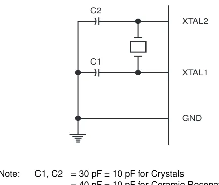
XTAL1
Input to the inverting oscillator amplifier and input to the internal clock operating circuit.
XTAL2
Output from the inverting oscillator amplifier.
Oscillator Characteristics
XTAL1 and XTAL2 are the input and output, respectively, of an inverting amplifier which can be configured for use as an on-chip oscillator, as shown in Figure 1. Either a quartz crystal or ceramic resonator may be used. To drive the device from an external clock source, XTAL2 should be left unconnected while XTAL1 is driven as shown in Figure 2. There are no requirements on the duty cycle of the external clock signal, since the input to the internal clocking circuitry is through a divide-by-two flip-flop, but minimum and maxi-mum voltage high and low time specifications must be observed.
Idle Mode
In idle mode, the CPU puts itself to sleep while all the on-chip peripherals remain active. The mode is invoked by software. The content of the on-chip RAM and all the spe-cial functions registers remain unchanged during this mode. The idle mode can be terminated by any enabled interrupt or by a hardware reset.
It should be noted that when idle is terminated by a hard ware reset, the device normally resumes program execu-tion, from where it left off, up to two machine cycles before the internal reset algorithm takes control. On-chip hardware inhibits access to internal RAM in this event, but access to the port pins is not inhibited. To eliminate the possibility of an unexpected write to a port pin when Idle is terminated by reset, the instruction following the one that invokes Idle should not be one that writes to a port pin or to external memory.
Figure 1. Oscillator Connections
Note: C1, C2 = 30 pF ± 10 pF for Crystals
= 40 pF ± 10 pF for Ceramic Resonators
Figure 2. External Clock Drive Configuration
C2
XTAL2
GND XTAL1 C1
Status of External Pins During Idle and Power Down Modes
Mode Program Memory ALE PSEN PORT0 PORT1 PORT2 PORT3
Power Down Mode
In the power down mode the oscillator is stopped, and the instruction that invokes power down is the last instruction executed. The on-chip RAM and Special Function Regis-ters retain their values until the power down mode is termi-nated. The only exit from power down is a hardware reset. Reset redefines the SFRs but does not change the on-chip
RAM. The reset should not be activated before VCC is
restored to its normal operating level and must be held active long enough to allow the oscillator to restart and sta-bilize.
Program Memory Lock Bits
On the chip are three lock bits which can be left unpro-grammed (U) or can be prounpro-grammed (P) to obtain the addi-tional features listed in the table below:
When lock bit 1 is programmed, the logic level at the EA pin is sampled and latched during reset. If the device is pow-ered up without a reset, the latch initializes to a random value, and holds that value until reset is activated. It is nec-essary that the latched value of EA be in agreement with the current logic level at that pin in order for the device to function properly.
Lock Bit Protection Modes
Program Lock Bits Protection Type LB1 LB2 LB3
1 U U U No program lock features.
2 P U U MOVC instructions executed from external program memory are disabled from fetching code bytes from internal memory, EA is sampled and latched on reset, and further programming of the Flash is disabled.
3 P P U Same as mode 2, also verify is disabled.
4 P P P Same as mode 3, also external execution is disabled.
Programming the Flash
The AT89C51 is normally shipped with the on-chip Flash memory array in the erased state (that is, contents = FFH) and ready to be programmed. The programming interface accepts either a high-voltage (12-volt) or a low-voltage
(VCC) program enable signal. The low voltage
program-ming mode provides a convenient way to program the AT89C51 inside the user’s system, while the high-voltage programming mode is compatible with conventional third party Flash or EPROM programmers.
The AT89C51 is shipped with either the high-voltage or low-voltage programming mode enabled. The respective top-side marking and device signature codes are listed in the following table.
The AT89C51 code memory array is programmed
byte-by-byte in either programming mode. To program any
non-blank byte in the on-chip Flash Memory, the entire memory must be erased using the Chip Erase Mode.
Programming Algorithm: Before programming the
AT89C51, the address, data and control signals should be set up according to the Flash programming mode table and Figures 3 and 4. To program the AT89C51, take the follow-ing steps.
1. Input the desired memory location on the address
lines.
2. Input the appropriate data byte on the data lines.
3. Activate the correct combination of control signals.
4. Raise EA/VPP to 12V for the high-voltage programming
mode.
5. Pulse ALE/PROG once to program a byte in the Flash
array or the lock bits. The byte-write cycle is self-timed and typically takes no more than 1.5 ms. Repeat steps 1 through 5, changing the address and data for the entire array or until the end of the object file is reached. Data Polling: The AT89C51 features Data Polling to indi-cate the end of a write cycle. During a write cycle, an attempted read of the last byte written will result in the com-plement of the written datum on PO.7. Once the write cycle has been completed, true data are valid on all outputs, and the next cycle may begin. Data Polling may begin any time after a write cycle has been initiated.
Ready/Busy: The progress of byte programming can also be monitored by the RDY/BSY output signal. P3.4 is pulled low after ALE goes high during programming to indicate BUSY. P3.4 is pulled high again when programming is done to indicate READY.
VPP = 12V VPP = 5V
Program Verify: If lock bits LB1 and LB2 have not been programmed, the programmed code data can be read back via the address and data lines for verification. The lock bits cannot be verified directly. Verification of the lock bits is achieved by observing that their features are enabled. Chip Erase: The entire Flash array is erased electrically by using the proper combination of control signals and by holding ALE/PROG low for 10 ms. The code array is written with all “1”s. The chip erase operation must be executed before the code memory can be re-programmed.
Reading the Signature Bytes: The signature bytes are read by the same procedure as a normal verification of locations 030H,
031H, and 032H, except that P3.6 and P3.7 must be pulled to a logic low. The values returned are as follows.
(030H) = 1EH indicates manufactured by Atmel (031H) = 51H indicates 89C51
(032H) = FFH indicates 12V programming (032H) = 05H indicates 5V programming
Programming Interface
Every code byte in the Flash array can be written and the entire array can be erased by using the appropriate combi-nation of control signals. The write operation cycle is self-timed and once initiated, will automatically time itself to completion.
All major programming vendors offer worldwide support for the Atmel microcontroller series. Please contact your local programming vendor for the appropriate software revision.
Flash Programming Modes
Note: 1. Chip Erase requires a 10-ms PROG pulse.
Mode RST PSEN ALE/PROG EA/VPP P2.6 P2.7 P3.6 P3.7
Write Code Data H L H/12V L H H H
Read Code Data H L H H L L H H
Write Lock Bit - 1 H L H/12V H H H H
Bit - 2 H L H/12V H H L L
Bit - 3 H L H/12V H L H L
Chip Erase H L H/12V H L L L
Read Signature Byte H L H H L L L L
Figure 3. Programming the Flash Figure 4. Verifying the Flash
P1
P2.6
P3.6 P2.0 - P2.3 A0 - A7
ADDR. OOOOH/OFFFH
T SEE FLASH PROGRAMMING
MODES ABLE
3-24 MHz
A8 - A11 P0
+5V
P2.7
PGM DATA
PROG
V /VIH PP
VIH
ALE
P3.7
XTAL2 EA
RST PSEN XTAL1
GND
VCC AT89C51
P1
P2.6
P3.6 P2.0 - P2.3 A0 - A7
ADDR. OOOOH/0FFFH
3-24 MHz
A8 - A11
P0
+5V
P2.7
PGM DATA (USE 10K PULLUPS)
VIH VIH
ALE
P3.7
XTAL2 EA
RST PSEN XTAL1
GND
VCC AT89C51
T SEE FLASH PROGRAMMING
MODES ABLE
Flash Programming and Verification Characteristics
TA = 0°C to 70°C, VCC = 5.0 ± 10%
Note: 1. Only used in 12-volt programming mode.
Symbol Parameter Min Max Units
VPP(1) Programming Enable Voltage 11.5 12.5 V
IPP(1) Programming Enable Current 1.0 mA
1/tCLCL Oscillator Frequency 3 24 MHz
tAVGL Address Setup to PROG Low 48tCLCL
tGHAX Address Hold After PROG 48tCLCL
tDVGL Data Setup to PROG Low 48tCLCL
tGHDX Data Hold After PROG 48tCLCL
tEHSH P2.7 (ENABLE) High to VPP 48tCLCL
tSHGL VPP Setup to PROG Low 10 µs
tGHSL(1) VPP Hold After PROG 10 µs
tGLGH PROG Width 1 110 µs
tAVQV Address to Data Valid 48tCLCL
tELQV ENABLE Low to Data Valid 48tCLCL
tEHQZ Data Float After ENABLE 0 48tCLCL
tGHBL PROG High to BUSY Low 1.0 µs
Flash Programming and Verification Waveforms - High Voltage Mode (V
PP
= 12V)
tGLGH tGHSL
tAVGL tSHGL
tDVGL
tGHAX
tAVQV tGHDX
tEHSH
tELQV
tWC
BUSY READY
tGHBL
tEHQZ P1.0 - P1.7
P2.0 - P2.3
ALE/PROG PORT 0
LOGIC 1 LOGIC 0
EA/VPP
VPP
P2.7 (ENABLE)
P3.4 (RDY/BSY)
PROGRAMMING ADDRESS
VERIFICATION ADDRESS
DATA IN DATA OUT
Flash Programming and Verification Waveforms - Low Voltage Mode (V
PP
= 5V)
tGLGH tAVGL
tSHGL
tDVGL
tGHAX
tAVQV tGHDX
tEHSH
tELQV
tWC
BUSY READY
tGHBL
tEHQZ P1.0 - P1.7
P2.0 - P2.3
ALE/PROG PORT 0
LOGIC 1 LOGIC 0
EA/VPP P2.7 (ENABLE)
P3.4 (RDY/BSY)
PROGRAMMING ADDRESS
VERIFICATION ADDRESS
Absolute Maximum Ratings*
DC Characteristics
TA = -40°C to 85°C, VCC = 5.0V ± 20% (unless otherwise noted)
Notes: 1. Under steady state (non-transient) conditions, IOL must be externally limited as follows: Maximum IOL per port pin: 10 mA
Maximum IOL per 8-bit port: Port 0: 26 mA Ports 1, 2, 3: 15 mA Maximum total IOL for all output pins: 71 mA
If IOL exceeds the test condition, VOL may exceed the related specification. Pins are not guaranteed to sink current greater
than the listed test conditions. 2. Minimum VCC for Power Down is 2V.
Operating Temperature ... -55°C to +125°C *NOTICE: Stresses beyond those listed under “Absolute Maximum Ratings” may cause permanent dam-age to the device. This is a stress rating only and functional operation of the device at these or any other conditions beyond those indicated in the operational sections of this specification is not implied. Exposure to absolute maximum rating conditions for extended periods may affect device reliability.
Storage Temperature ... -65°C to +150°C Voltage on Any Pin
with Respect to Ground ...-1.0V to +7.0V Maximum Operating Voltage... 6.6V DC Output Current... 15.0 mA
Symbol Parameter Condition Min Max Units
VIL Input Low Voltage (Except EA) -0.5 0.2 VCC - 0.1 V VIL1 Input Low Voltage (EA) -0.5 0.2 VCC - 0.3 V VIH Input High Voltage (Except XTAL1, RST) 0.2 VCC + 0.9 VCC + 0.5 V VIH1 Input High Voltage (XTAL1, RST) 0.7 VCC VCC + 0.5 V VOL Output Low Voltage(1) (Ports 1,2,3) IOL = 1.6 mA 0.45 V VOL1 Output Low Voltage(1)
(Port 0, ALE, PSEN)
IOL = 3.2 mA 0.45 V
VOH Output High Voltage (Ports 1,2,3, ALE, PSEN)
IOH = -60 µA, VCC = 5V ± 10% 2.4 V
IOH = -25 µA 0.75 VCC V
IOH = -10 µA 0.9 VCC V
VOH1 Output High Voltage
(Port 0 in External Bus Mode)
IOH = -800 µA, VCC = 5V ± 10% 2.4 V
IOH = -300 µA 0.75 VCC V
IOH = -80 µA 0.9 VCC V
IIL Logical 0 Input Current (Ports 1,2,3) VIN = 0.45V -50 µA ITL Logical 1 to 0 Transition Current
(Ports 1,2,3)
VIN = 2V, VCC = 5V ± 10% -650 µA ILI Input Leakage Current (Port 0, EA) 0.45 < VIN < VCC ±10 µA
RRST Reset Pulldown Resistor 50 300 KΩ
CIO Pin Capacitance Test Freq. = 1 MHz, TA = 25°C 10 pF ICC Power Supply Current Active Mode, 12 MHz 20 mA
Idle Mode, 12 MHz 5 mA
Power Down Mode(2) VCC = 6V 100 µA
AC Characteristics
(Under Operating Conditions; Load Capacitance for Port 0, ALE/PROG, and PSEN = 100 pF; Load Capacitance for all other outputs = 80 pF)
External Program and Data Memory Characteristics
Symbol Parameter 12 MHz Oscillator 16 to 24 MHz Oscillator Units
Min Max Min Max
1/tCLCL Oscillator Frequency 0 24 MHz
tLHLL ALE Pulse Width 127 2tCLCL-40 ns
tAVLL Address Valid to ALE Low 43 tCLCL-13 ns
tLLAX Address Hold After ALE Low 48 tCLCL-20 ns
tLLIV ALE Low to Valid Instruction In 233 4tCLCL-65 ns
tLLPL ALE Low to PSEN Low 43 tCLCL-13 ns
tPLPH PSEN Pulse Width 205 3tCLCL-20 ns
tPLIV PSEN Low to Valid Instruction In 145 3tCLCL-45 ns
tPXIX Input Instruction Hold After PSEN 0 0 ns
tPXIZ Input Instruction Float After PSEN 59 tCLCL-10 ns
tPXAV PSEN to Address Valid 75 tCLCL-8 ns
tAVIV Address to Valid Instruction In 312 5tCLCL-55 ns
tPLAZ PSEN Low to Address Float 10 10 ns
tRLRH RD Pulse Width 400 6tCLCL-100 ns
tWLWH WR Pulse Width 400 6tCLCL-100 ns
tRLDV RD Low to Valid Data In 252 5tCLCL-90 ns
tRHDX Data Hold After RD 0 0 ns
tRHDZ Data Float After RD 97 2tCLCL-28 ns
tLLDV ALE Low to Valid Data In 517 8tCLCL-150 ns
tAVDV Address to Valid Data In 585 9tCLCL-165 ns
tLLWL ALE Low to RD or WR Low 200 300 3tCLCL-50 3tCLCL+50 ns
tAVWL Address to RD or WR Low 203 4tCLCL-75 ns
tQVWX Data Valid to WR Transition 23 tCLCL-20 ns
tQVWH Data Valid to WR High 433 7tCLCL-120 ns
tWHQX Data Hold After WR 33 tCLCL-20 ns
tRLAZ RD Low to Address Float 0 0 ns
External Program Memory Read Cycle
External Data Memory Read Cycle
tLHLL
tLLIV tPLIV
tLLAX tPXIZ
tPLPH
tPLAZ tPXAV tAVLL
tLLPL
tAVIV
tPXIX ALE
PSEN
PORT 0
PORT 2 A8 - A15
A0 - A7 A0 - A7
A8 - A15 INSTR IN
tLHLL
tLLDV
tLLWL
tLLAX
tWHLH
tAVLL
tRLRH
tAVDV
tAVWL
tRLAZ t
RHDX
tRLDV tRHDZ
A0 - A7 FROM RI OR DPL
ALE PSEN
RD
PORT 0
PORT 2 P2.0 - P2.7 OR A8 - A15 FROM DPH
A0 - A7 FROM PCL
A8 - A15 FROM PCH
External Data Memory Write Cycle
External Clock Drive Waveforms
External Clock Drive
Symbol Parameter Min Max Units
1/tCLCL Oscillator Frequency 0 24 MHz
tCLCL Clock Period 41.6 ns
tCHCX High Time 15 ns
tCLCX Low Time 15 ns
tCLCH Rise Time 20 ns
tCHCL Fall Time 20 ns
tLHLL
tLLWL
tLLAX
tWHLH
tAVLL
tWLWH
tAVWL
tQVWX
tQVWH
tWHQX
A0 - A7 FROM RI OR DPL
ALE PSEN
WR
PORT 0
PORT 2 P2.0 - P2.7 OR A8 - A15 FROM DPH
A0 - A7 FROM PCL
A8 - A15 FROM PCH
DATA OUT INSTR IN
tCHCX tCHCX
tCLCX
tCLCL
tCHCL tCLCH
V - 0.5VCC
0.45V
Serial Port Timing: Shift Register Mode Test Conditions
(VCC = 5.0 V ± 20%; Load Capacitance = 80 pF)
Shift Register Mode Timing Waveforms
Symbol Parameter 12 MHz Osc Variable Oscillator Units
Min Max Min Max
tXLXL Serial Port Clock Cycle Time 1.0 12tCLCL µs
tQVXH Output Data Setup to Clock Rising Edge 700 10tCLCL-133 ns tXHQX Output Data Hold After Clock Rising Edge 50 2tCLCL-117 ns
tXHDX Input Data Hold After Clock Rising Edge 0 0 ns
tXHDV Clock Rising Edge to Input Data Valid 700 10tCLCL-133 ns
tXHDV
tQVXH
tXLXL
tXHDX tXHQX
ALE
INPUT DATA CLEAR RI OUTPUT DATA WRITE TO SBUF INSTRUCTION
CLOCK
0
0 1
1 2
2 3
3 4
4 5
5 6
6 7
7
SET TI
SET RI 8
VALID VALID VALID VALID VALID VALID VALID VALID
Float Waveforms
(1)
Note: 1. For timing purposes, a port pin is no longer floating when a 100 mV change from load voltage occurs. A port pin begins to float when 100 mV change from the loaded VOH/VOL level occurs.
VLOAD+ 0.1V
Timing Reference Points V
LOAD- 0.1V LOAD
V VOL+ 0.1V
VOL- 0.1V
AC Testing Input/Output Waveforms
(1)
Note: 1. AC Inputs during testing are driven at VCC - 0.5V for
a logic 1 and 0.45V for a logic 0. Timing measure-ments are made at VIH min. for a logic 1 and VIL
max. for a logic 0. 0.45V
TEST POINTS V - 0.5VCC
0.2 V + 0.9VCC
Ordering Information
Speed (MHz)
Power
Supply Ordering Code Package Operation Range
12 5V ± 20% AT89C51-12AC 44A Commercial
AT89C51-12JC 44J (0°C to 70°C)
AT89C51-12PC 40P6
AT89C51-12QC 44Q
AT89C51-12AI 44A Industrial
AT89C51-12JI 44J (-40°C to 85°C)
AT89C51-12PI 40P6
AT89C51-12QI 44Q
AT89C51-12AA 44A Automotive
AT89C51-12JA 44J (-40°C to 105°C)
AT89C51-12PA 40P6
AT89C51-12QA 44Q
16 5V ± 20% AT89C51-16AC 44A Commercial
AT89C51-16JC 44J (0°C to 70°C)
AT89C51-16PC 40P6
AT89C51-16QC 44Q
AT89C51-16AI 44A Industrial
AT89C51-16JI 44J (-40°C to 85°C)
AT89C51-16PI 40P6
AT89C51-16QI 44Q
AT89C51-16AA 44A Automotive
AT89C51-16JA 44J (-40°C to 105°C)
AT89C51-16PA 40P6
AT89C51-16QA 44Q
20 5V ± 20% AT89C51-20AC 44A Commercial
AT89C51-20JC 44J (0°C to 70°C)
AT89C51-20PC 40P6
AT89C51-20QC 44Q
AT89C51-20AI 44A Industrial
AT89C51-20JI 44J (-40°C to 85°C)
AT89C51-20PI 40P6
Ordering Information
Speed (MHz)
Power
Supply Ordering Code Package Operation Range
24 5V ± 20% AT89C51-24AC 44A Commercial
AT89C51-24JC 44J (0°C to 70°C)
AT89C51-24PC 44P6
AT89C51-24QC 44Q
AT89C51-24AI 44A Industrial
AT89C51-24JI 44J (-40°C to 85°C)
AT89C51-24PI 44P6
AT89C51-24QI 44Q
Package Type 44A 44 Lead, Thin Plastic Gull Wing Quad Flatpack (TQFP)
44J 44 Lead, Plastic J-Leaded Chip Carrier (PLCC)
40P6 40 Lead, 0.600” Wide, Plastic Dual Inline Package (PDIP)
SEMICONDUCTOR TECHNICAL DATA
OCTAL PERIPHERAL
DRIVER ARRAYS
PIN CONNECTIONS
Order this document by ULN2803/D
A SUFFIX
PLASTIC PACKAGE CASE 707
6
9 8 7 5 4 3 2 1
10 11 12 13 14 15 16 17 18
Gnd
The eight NPN Darlington connected transistors in this family of arrays are ideally suited for interfacing between low logic level digital circuitry (such as TTL, CMOS or PMOS/NMOS) and the higher current/voltage requirements of lamps, relays, printer hammers or other similar loads for a broad range of computer, industrial, and consumer applications. All devices feature open–collector outputs and free wheeling clamp diodes for transient suppression.
The ULN2803 is designed to be compatible with standard TTL families while the ULN2804 is optimized for 6 to 15 volt high level CMOS or PMOS.
MAXIMUM RATINGS(TA = 25°C and rating apply to any one device in the package, unless otherwise noted.)
Rating Symbol Value Unit
Output Voltage VO 50 V
Input Voltage (Except ULN2801) VI 30 V Collector Current – Continuous IC 500 mA Base Current – Continuous IB 25 mA Operating Ambient Temperature Range TA 0 to +70 °C Storage Temperature Range Tstg – 55 to +150 °C Junction Temperature TJ 125 °C
RθJA = 55°C/W
Do not exceed maximum current limit per driver.
ORDERING INFORMATION
D i
Characteristics Device
Input
Compatibility VCE(Max)/IC(Max)
Operating Temperature
Range
ULN2803A TTL, 5.0 V CMOS
Output Leakage Current (Figure 1) (VO = 50 V, TA = +70°C) (VO = 50 V, TA = +25°C)
(VO = 50 V, TA = +70°C, VI = 6.0 V) (VO = 50 V, TA = +70°C, VI = 1.0 V)
All Types All Types ULN2802 ULN2804 ICEX – – – – – – – – 100 50 500 500 µA
Collector–Emitter Saturation Voltage (Figure 2) (IC = 350 mA, IB = 500 µA)
(IC = 200 mA, IB = 350 µA) (IC = 100 mA, IB = 250 µA)
All Types All Types All Types VCE(sat) – – – 1.1 0.95 0.85 1.6 1.3 1.1 V
Input Current – On Condition (Figure 4) (VI = 17 V)
(VI = 3.85 V) (VI = 5.0 V) (VI = 12 V)
ULN2802 ULN2803 ULN2804 ULN2804 II(on) – – – – 0.82 0.93 0.35 1.0 1.25 1.35 0.5 1.45 mA
Input Voltage – On Condition (Figure 5) (VCE = 2.0 V, IC = 300 mA) (VCE = 2.0 V, IC = 200 mA) (VCE = 2.0 V, IC = 250 mA) (VCE = 2.0 V, IC = 300 mA) (VCE = 2.0 V, IC = 125 mA) (VCE = 2.0 V, IC = 200 mA) (VCE = 2.0 V, IC = 275 mA) (VCE = 2.0 V, IC = 350 mA)
ULN2802 ULN2803 ULN2803 ULN2803 ULN2804 ULN2804 ULN2804 ULN2804 VI(on) – – – – – – – – – – – – – – – – 13 2.4 2.7 3.0 5.0 6.0 7.0 8.0 V
Input Current – Off Condition (Figure 3) (IC = 500 µA, TA = +70°C)
All Types II(off) 50 100 – µA DC Current Gain (Figure 2)
(VCE = 2.0 V, IC = 350 mA)
ULN2801 hFE 1000 – – –
Input Capacitance CI – 15 25 pF
Turn–On Delay Time (50% EI to 50% EO)
ton – 0.25 1.0 µs
Turn–Off Delay Time (50% EI to 50% EO)
toff – 0.25 1.0 µs
Clamp Diode Leakage Current (Figure 6) (VR = 50 V)
TA = +25°C TA = +70°C
IR – – 50
100
µA Clamp Diode Forward Voltage (Figure 7)
(IF = 350 mA)
ULN2803 ULN2804
IC VCE
Open
µA
Open ICEX
DUT
V DUT
Open
Vin
VCE
IF V V
IC
µA
DUT
IR VR
DUT
Open
VCE
Open
Vin V
TEST FIGURES
VCE Open
µA
DUT
µA Vin
Iin
hFE+IIC in
(See Figure Numbers in Electrical Characteristics Table)
Open DUT
Open
Vin
µA
Figure 1. Figure 2.
Figure 3. Figure 4.
Figure 5. Figure 6.
200
2.0 5.0
VIN, INPUT VOLTAGE (V)
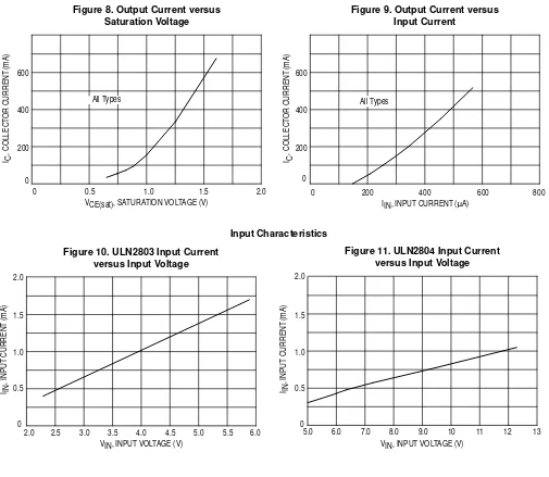
12 11 10 9.0 8.0 7.0 6.0 0 0.5 1.0 1.5 2.0 6.0 5.5 5.0 4.5 3.5 4.0 3.0 2.5 0 2.0 0.5 1.0 All Types
IIN, INPUT CURRENT (µA)
800 600 400 200 0 0 200 400 0.5 600 2.0 1.5 0 1.0 All Types 0 600 400
VCE(sat), SATURATION VOLTAGE (V)
1.5
VIN, INPUT VOLTAGE (V)
Input Characteristics Figure 8. Output Current versus
Saturation Voltage
I , INPUT
CURRENT
(mA)
IN I , INPUT
CURRENT
(mA)
IN
I , COLLECT
OR
CURRENT
(mA)
C I , COLLECT
OR
CURRENT
(mA)
C
Figure 9. Output Current versus Input Current
Figure 10. ULN2803 Input Current versus Input Voltage
Figure 11. ULN2804 Input Current versus Input Voltage
13 2.7 k 7.2 k 3.0 k Pin 10 1/8 ULN2803 3.0 k 7.2 k 10.5 k 1/8 ULN2804
Figure 12. Representative Schematic Diagrams
ULN2803 ULN2804
OUTLINE DIMENSIONS
NOTES:
1. POSITIONAL TOLERANCE OF LEADS (D), SHALL BE WITHIN 0.25 (0.010) AT MAXIMUM MATERIAL CONDITION, IN RELATION TO SEATING PLANE AND EACH OTHER. 2. DIMENSION L TO CENTER OF LEADS WHEN
FORMED PARALLEL.
3. DIMENSION B DOES NOT INCLUDE MOLD FLASH.
1
SEATING PLANE 10
9 18
M A
B
K C N F
G D H
J
L DIM MIN MAX MIN MAX
INCHES MILLIMETERS
A 22.22 23.24 0.875 0.915 B 6.10 6.60 0.240 0.260 C 3.56 4.57 0.140 0.180 D 0.36 0.56 0.014 0.022 F 1.27 1.78 0.050 0.070 G 2.54 BSC 0.100 BSC H 1.02 1.52 0.040 0.060 J 0.20 0.30 0.008 0.012 K 2.92 3.43 0.115 0.135 L 7.62 BSC 0.300 BSC M 0 15 0 15 N 0.51_ 1.02_ 0.020_ 0.040_
A SUFFIX
PLASTIC PACKAGE CASE 707–02
6 MOTOROLA ANALOG IC DEVICE DATA
Motorola reserves the right to make changes without further notice to any products herein. Motorola makes no warranty, representation or guarantee regarding the suitability of its products for any particular purpose, nor does Motorola assume any liability arising out of the application or use of any product or circuit, and specifically disclaims any and all liability, including without limitation consequential or incidental damages. “Typical” parameters which may be provided in Motorola data sheets and/or specifications can and do vary in different applications and actual performance may vary over time. All operating parameters, including “Typicals” must be validated for each customer application by customer’s technical experts. Motorola does not convey any license under its patent rights nor the rights of others. Motorola products are not designed, intended, or authorized for use as components in systems intended for surgical implant into the body, or other applications intended to support or sustain life, or for any other application in which the failure of the Motorola product could create a situation where personal injury or death may occur. Should Buyer purchase or use Motorola products for any such unintended or unauthorized application, Buyer shall indemnify and hold Motorola and its officers, employees, subsidiaries, affiliates, and distributors harmless against all claims, costs, damages, and expenses, and reasonable attorney fees arising out of, directly or indirectly, any claim of personal injury or death associated with such unintended or unauthorized use, even if such claim alleges that Motorola was negligent regarding the design or manufacture of the part. Motorola and are registered trademarks of Motorola, Inc. Motorola, Inc. is an Equal Opportunity/Affirmative Action Employer.
How to reach us:
USA / EUROPE / Locations Not Listed: Motorola Literature Distribution; JAPAN: Nippon Motorola Ltd.; Tatsumi–SPD–JLDC, 6F Seibu–Butsuryu–Center,
P.O. Box 20912; Phoenix, Arizona 85036. 1–800–441–2447 or 602–303–5454 3–14–2 Tatsumi Koto–Ku, Tokyo 135, Japan. 03–81–3521–8315
MFAX: [email protected] – TOUCHTONE 602–244–6609 ASIA/PACIFIC: Motorola Semiconductors H.K. Ltd.; 8B Tai Ping Industrial Park,
INTERNET: http://Design–NET.com 51 Ting Kok Road, Tai Po, N.T., Hong Kong. 852–26629298
ULN2803/D
*ULN2803/D*
LAMPIRAN C
org 0h
main: mov p0,#00h
mov p1,#00h
mov p2,#00h
cari: jb p1.1,kanan
jb p1.0,kiri
sjmp cari
kiri: call sch
mov p2,#08h
call sch
call delay
call sch
mov p2,#04h
call sch
call delay
call sch
mov p2,#02h
call sch
call delay
call sch
mov p2,#01h
call sch
call delay
call sch
sjmp kiri
kanan:call sch
mov p2,#04h
call sch
call delay
call sch
mov p2,#08h
call sch
call delay
call sch
sjmp kanan
sch: mov a,p1
cjne a,#03h,awal
sjmp cari
awal: ret
delay: call sch
mov r0,#20h
call sch
dly0: mov r1,#20h
call sch
dly1: mov r2,#20h
call sch
dly2: djnz r2,dly2
call sch
djnz r1,dly1
call sch
djnz r0,dly0
call sch
BAB I
PENDAHULUAN
1.1 Latar Belakang
Dalam bidang keamanan, kamera sering digunakan untuk memantau keadaan
suatu tempat. Keterbatasan kamera terletak pada batasan sudut jangkauan cakupan,
sehingga ketika objek berada di luar jangkauan, kamera akan diarahkan pada objek
tersebut. Salah satu objek yang memancarkan sinar infrared dan dipantau oleh kamera
adalah manusia. Perbedaan temperatur pada permukaan kulit manusia dengan
sekitarnya yang menjadi acuan bagi sensor infrared sehingga dapat membedakan
objek mana yang akan diikuti pergerakannya.
Dalam tugas akhir ini akan dirancang dan direalisasikan sebuah alat yang
dapat mendeteksi infrared dan dapat mengikuti pergerakan horisontal sumber infrared
tersebut.
1.2 Identifikasi Masalah
Pada pembuatan alat, permasalahan difokuskan pada bagaimana membuat
sebuah alat pendeteksi sumber sinar infrared dan bagaimana membuat alat tersebut
Tujuan dari Tugas Akhir ini adalah membuat sebuah alat yang dapat
menemukan benda yang mengeluarkan sinar infrared.
1.2 Metoda Penelitian
Dalam penulisan Laporan Tugas Akhir ini metoda penelitian yang digunakan
adalah :
•
Studi Literatur, dilaksanakan untuk mengetahui definisi dan
karakteristik perangkat yang dipakai.
•
Membuat alat, dilaksanakan untuk memperoleh data-data yang
diperlukan dan mengetahui secara langsung proses kerja alat tersebut.
1.3 Pembatasan Masalah
Dalam pembuatan alat ini, permasalahan akan dibatasi pada :
•
Alat hanya dapat berotasi horisontal
•
Alat hanya berupa prototype
•
Sumber infrared diasumsikan hanya berupa 1 titik
1.1 Sistematika Pembahasan
Penulisan laporan Tugas Akhir ini secara garis besar terbagi ke dalam lima
bab, yaitu :
Bab I
:
Pendahuluan
Berisi latar belakang, identifikasi masalah, tujuan, metoda
penelitian, pembatasan masalah, dan sistematika
pembahasan.
Bab II
:
Teori Penunjang
Berisi teori dasar mengenai mikrokontroler AT89C51,
sinar infrared, sensor cahaya, dan motor stepper.
Bab III
:
Perancangan dan Realisasi Alat
Berisi diagram blok, cara kerja alat, perancangan dan
pembuatan perangkat keras maupun perangkat lunak pada
mikrokontroler.
Bab IV
:
Pengujian Alat dan Data Pengamatan
Berisi penjelasan tentang percobaan yang dilakukan untuk
menguji perangkat keras dan perangkat lunak yang telah
dibuat.
Bab V
:
Kesimpulan dan Saran
Berisi kesimpulan dan saran yang didapat dari percobaan
dan pengujian yang dilakukan.
KESIMPULAN DAN SARAN
Bab ini menjelaskan tentang kesimpulan dan saran yang diperoleh dari percobaan dan pengujian
alat.
5.1. Kesimpulan
Berdasarkan percobaan dan pengamatan yang telah dilakukan dalam tugas akhir ini
dapat disimpulkan bahwa:
1.
Alat yang direalisasikan yaitu alat yang dapat mendeteksi sumber infrared
dan mengikuti pergerakan horisontalnya dapat bekerja dengan baik.
2.
Jarak sumber infrared berupa
remote control
yang dapat terdeteksi oleh sistem
sensor mencapai 800 cm terhadap sumbu tegak dengan sudut jangkauan cakupan
17,35°.
3.
Jarak terjauh sumber infrared berupa lampu 5 watt yang dapat terdeteksi
oleh sistem sensor adalah 12 cm terhadap sumbu tegak dengan sudut jangkauan
cakupan 14,03° dan 3 cm pada sudut 45°.
4.
Waktu respon yang dibutuhkan sistem sensor untuk mencapai satu posisi
tertentu sumber infared adalah berbanding lurus karena kecepatan pergeseran
5.2. Saran
Untuk pengembangan selanjutnya, disarankan agar:
1.
Alat dapat berotasi secara vertikal dan horisontal.
2.