i
PEMBUATAN PERANGKAT LUNAK BERBASIS DIAGRAM
ALIR UNTUK MENGONTROL ROBOT
Disusun Oleh:
Willy Yohannes
0422039
Jurusan Teknik Elektro, Fakultas Teknik, Universitas Kristen Maranatha,
Jl. Prof.Drg.Suria Sumantri, MPH no.65, Bandung, Indonesia,
email : [email protected]
ABSTRAK
Robotik merupakan salah satu bidang ilmu dalam dunia pendidikan yang
banyak diminati. Teori robotik banyak digunakan sebagai sarana pembelajaran
dalam dunia pendidikan, yang meliputi logika berpikir, pemecahan masalah, dan
penerapannya. Konsep dasar dari teori robotik diterapkan salah satunya melalui
bahasa pemograman.
Diagram alir merupakan diagram yang menguraikan langkah-langkah
penyelesaian suatu masalah. Langkah-langkah penyelesaian pada diagram alir
menggunakan simbol-simbol khusus yang mudah dimengerti. Dengan diagram
alir, dasar-dasar bahasa pemrograman menjadi lebih mudah dipahami.
Pada Tugas Akhir ini, dibuat suatu perangkat lunak berbasis diagram alir
dengan simbol-simbol dari tiap blok diagram memiliki perintah yang digunakan
untuk menggerakkan robot. Perintah ini berupa
source code
yang dikirim dari PC
ke mikrokontroler AT89S52. Mikrokontroler menampilkan simulasi berdasarkan
diagram alir yang dibuat pada perangkat lunak. Simulasi output dari perangkat
lunak ditunjukkan pada port 0 mikrokontroler, sedangkan simulasi input dari
perangkat lunak ditunjukkan pada port 1 mikrokontroler.
ii
iii
MAKING OF SOFTWARE BASED ON FLOWCHART FOR CONTROLLING
ROBOT
Composed by:
Willy Yohannes
0422039
Electrical Engineering, Maranatha Cristian University,
Jl. Prof.Drg.Suria Sumantri, MPH no.65, Bandung, Indonesia,
email : [email protected]
ABSTRACT
Robotic is one of the science area in the world of education which
enthused many. Theory of robotic used as study media in the world of education,
covering logic thinking, problem solving, and applying of. Basic concept of
robotic is applied for language of programme
Flowchart is diagram which elaborating steps of problem solution. Steps at
flowchart using special symbols which is easy to understood. With flowchart,
bases language of programme become comprehended easier.
At This Final Project, has been made a software based on flowchart with
symbols of each diagram block have command which is used for controlling
robot. This command is source code which is sent from PC to AT89S52
microcontroller. Microcontroller present simulation based on flowchart which is
made at software. Simulation of output from the software is shown at port 0 of
microcontroller, simulation of input from the software is shown at port 1 of
microcontroller.
vi
DAFTAR ISI
ABSTRAK ...i
ABSTRACT... iii
KATA PENGANTAR ...iv
DAFTAR ISI...vi
DAFTAR TABEL... ix
DAFTAR GAMBAR ... x
BAB I
PENDAHULUAN... 1
I.1
Latar Belakang ... 1
I.2
Identifikasi Masalah ... 1
I.3
Tujuan... 1
I.4
Pembatasan Masalah ... 2
I.5
Spesifikasi Alat... 2
I.6
Sistematika Penulisan... 2
BAB II
LANDASAN TEORI ... 4
II.1
Konsep Dasar Diagram Alir (flowchart)... 4
II.2
Pengenalan Visual Basic ... 6
II.2.1
Jenis
File
pada Visual Basic... 7
II.2.2
Komponen pada Visual Basic ... 7
II.2.3
Struktur aplikasi Visual Basic ... 8
II.2.4
Jenis data pada Visual Basic ...10
II.3
Komunikasi Serial ...12
II.4
Mikrokontroler ...14
II.4.1
Central Processing Unit (CPU) ...14
II.4.2
Bus Alamat ...15
II.4.3
Bus Data ...15
II.4.4
Bus Kontrol ...15
vii
II.4.6
RAM (Random Access Memory)...16
II.4.7
ROM (Read Only Memory) ...16
II.5
Mikrokontroler AT89S52...16
II.6
Pengenalan Robot...18
II.7
Motor DC ...19
II.8
Motor Stepper...21
BAB III
PERANGKAT LUNAK BERBASIS DIAGRAM ALIR ...24
III.1
Pendahuluan ...24
III.2
Definisi Blok Diagram ...24
III.2.1
Blok Diagram Start...24
III.2.2
Blok Diagram Input...25
III.2.3
Blok Diagram Conditional ...25
III.2.4
Blok Diagram Counter ...25
III.2.5
Blok Diagram Time Delay ...26
III.2.6
Blok Diagram Go To...26
III.2.7
Blok Diagram Output ...27
III.2.7.1
Motor DC ...27
III.2.7.1.1 Motor DC berputar searah jarum jam (Clockwise)...27
III.2.7.1.2 Motor DC berlawanan arah jarum jam (Counter Clockwise) ...28
III.2.7.1.3 Motor DC berhenti berputar ...28
III.2.7.2
Motor Stepper...29
III.2.8
Blok Diagram End...29
III.3
Perancangan Perangkat Lunak ...29
III.4
Cara Kerja Perangkat Lunak ...33
BAB IV
SIMULASI ...39
IV.1
Simulasi Input...39
IV.2
Simulasi Output...40
IV.3
Simulasi gerakan robot maju...41
viii
IV.5
Simulasi gerakan robot maju dengan posisi badan robot zig zag...43
IV.6
Simulasi gerakan robot menyerupai tanda plus (+)...44
IV.7
Simulasi gerakan robot menghindari objek dengan belok ke kanan ...45
BAB V
KESIMPULAN DAN SARAN...47
V.1
Kesimpulan...47
V.2
Saran...47
DAFTAR PUSTAKA
LAMPIRAN A LIST PROGRAM VISUAL BASIC
LAMPIRAN B BAHASA ASSEMBLER AT89S52
ix
DAFTAR TABEL
Tabel II.1 Simbol-simbol diagram alir ... 4
Tabel II.2 Konfigurasi pin pada konektor serial DB-9 ...13
Tabel II.3 Motor Stepper dengan Gerakan Full Step...22
Tabel II.4 Motor Stepper dengan Gerakan Half Step ...23
Tabel III.1 Properti dan setting timer...31
Tabel III.2 Properti dan setting MSComm...32
x
DAFTAR GAMBAR
Gambar II.1 Struktur aplikasi Visual Basic ... 8
Gambar II.2 Konektor Serial DB-9...13
Gambar II.3 IC AT89S52...17
Gambar II.4 Komunikasi AT89S52 dengan motor DC ...18
Gambar II.5 Struktur Robot ...19
Gambar II.6 Konfigurasi pin AT89S52 dengan Robot ...19
Gambar II.7 Motor DC...20
Gambar II.8 Kontruksi Motor Stepper dalam Satu Kali Putaran dengan Gerakan
Full Step ...22
Gambar II.9 Kontruksi Motor Stepper dalam Gerakan Half Step ...23
Gambar III.1 Blok diagram start ...24
Gambar III.2 Blok diagram Input...25
Gambar III.3 Blok diagram Conditional (if)...25
Gambar III.4 Blok diagram counter...25
Gambar III.5 Blok diagram time delay ...26
Gambar III.6 Blok diagram go to 1...26
Gambar III.7 Blok diagram go to 2...27
Gambar III.8 Blok diagram motor DC 1 berputar searah jarum jam
(clockwise) ...27
Gambar III.9 Blok diagram motor DC 2 berputar searah jarum jam
(clockwise) ...27
Gambar III.10 Blok diagram motor DC 1 berputar berlawanan arah jarum jam
(Counter Clockwise) ...28
Gambar III.11 Blok diagram motor DC 2 berputar berlawanan arah jarum jam
(Counter Clockwise) ...28
Gambar III.12 Blok diagram motor DC 1 berhenti berputar ...28
Gambar III.13 Blok diagram motor DC 2 berhenti berputar ...28
Gambar III.14 Blok diagram motor stepper...29
xi
Gambar III.16 Tampilan Perangkat Lunak ...30
Gambar III.17 Diagram Alir penggunaan perangkat lunak ...34
Gambar III.18 Diagram Alir dari subroutine “Motor”...35
Gambar III.19 Diagram Alir dari subroutine “Run” ...36
Gambar III.20 Diagram Alir dari subroutine “Sensor
Ø”
...37
Gambar IV.1 Struktur robot ...39
Gambar IV.2 Simulasi gerakan robot maju...41
Gambar IV.3 Simulasi gerakan robot maju, lalu berhenti ketika sensor
menunjukkan terdapat objek di depan robot ...42
Gambar IV.4 Simulasi gerakan robot maju dengan posisi badan robot zig zag ..43
Gambar IV.5 Simulasi gerakan robot menyerupai tanda plus (+) ...44
LAMPIRAN A
Dim a, aa, b, c, d, e, jj, m, n, o, x, xx, st1, st2, snr As Integer
Private Sub Command1_Click()
Command3.Visible = False
Command4.Visible = False
Picture2(0) = stt
Picture2(0).Visible = True
a = 1
b = 0
e = 0
xx = 0
snr = 0
mt1a = 0
mt1b = 0
mt2a = 0
mt2b = 0
For i = 1 To 36
Picture2(i) = useless
Picture2(i).Visible = False
Next
MSComm1.Output = Chr(0)
Timer2.Enabled = False
Timer3.Enabled = False
End Sub
Private Sub Command2_Click()
End
End Sub
Private Sub Command3_Click()
d = a
a = c
Command4.Visible = True
Command3.Visible = False
End Sub
Private Sub Command4_Click()
If (a - 13) > d Then
For i = d To (a - 13)
Picture2(i) = grs
Picture2(i).Visible = True
Next
a = a - 13
Else
a = d
End If
Private Sub Command5_Click()
e = 0
For i = 1 To 13
If Picture2(i) = motor1stop Then
If mt1a = 1 Then
e = e - 1
mt1a = 0
Timer1.Enabled = True
ElseIf mt1b = 1 Then
e = e - 2
mt1b = 0
Timer1.Enabled = True
End If
ElseIf Picture2(i) = motor2stop Then
If mt2a = 1 Then
e = e - 4
mt2a = 0
Timer1.Enabled = True
ElseIf mt2b = 1 Then
e = e - 8
mt2b = 0
Timer1.Enabled = True
End If
ElseIf Picture2(i) = motor1cw Then
e = e + 1
mt1a = 1
Timer1.Enabled = True
ElseIf Picture2(i) = motor1ccw Then
e = e + 2
mt1b = 1
Timer1.Enabled = True
ElseIf Picture2(i) = motor2cw Then
e = e + 4
mt2a = 1
Timer1.Enabled = True
ElseIf Picture2(i) = motor2ccw Then
e = e + 8
mt2b = 1
Timer1.Enabled = True
ElseIf Picture2(i) = inputs Then
Timer3.Enabled = True
ElseIf Picture2(i) = delay Then
Call Pause(jj)
ElseIf Picture2(i) = counter Then
xx = xx + 1
Timer1.Enabled = True
Text1.Text = xx
Command8.Visible = True
ElseIf Picture2(i) = gt2 Then
aa = i
Timer1.Enabled = True
ElseIf Picture2(i) = gt1 Then
i = aa
Timer1.Enabled = True
ElseIf Picture2(i) = ends Then
e = 0
Timer1.Enabled = True
ElseIf Picture2(i) = stepper Then
st1 = 4
st2 = 0
Timer2.Enabled = True
ElseIf Picture2(i) = ifs Then
If snr = 0 Then
For i2 = 14 To 26
If Picture2(i2) = motor1stop Then
If mt1a = 1 Then
e = e - 1
mt1a = 0
Timer1.Enabled = True
ElseIf mt1b = 1 Then
e = e - 2
mt1b = 0
Timer1.Enabled = True
End If
ElseIf Picture2(i2) = motor2stop Then
If mt2a = 1 Then
e = e - 4
mt2a = 0
Timer1.Enabled = True
ElseIf mt2b = 1 Then
e = e - 8
mt2b = 0
Timer1.Enabled = True
End If
ElseIf Picture2(i2) = motor1cw Then
e = e + 1
mt1a = 1
Timer1.Enabled = True
ElseIf Picture2(i2) = motor1ccw Then
e = e + 2
mt1b = 1
ElseIf Picture2(i2) = motor2cw Then
e = e + 4
mt2a = 1
Timer1.Enabled = True
ElseIf Picture2(i2) = motor2ccw Then
e = e + 8
mt2b = 1
Timer1.Enabled = True
ElseIf Picture2(i2) = inputs Then
Timer3.Enabled = True
ElseIf Picture2(i2) = delay Then
Call Pause(jj)
ElseIf Picture2(i2) = counter Then
xx = xx + 1
Text1.Visible = True
Timer1.Enabled = True
Text1.Text = xx
ElseIf Picture2(i2) = gt2 Then
aa = i
Timer1.Enabled = True
ElseIf Picture2(i2) = gt1 Then
i = aa
Timer1.Enabled = True
ElseIf Picture2(i2) = ends Then
e = 0
Timer1.Enabled = True
End
ElseIf Picture2(i2) = stepper Then
st1 = 4
st2 = 0
Timer2.Enabled = True
End If
Next
End If
End If
Next
End Sub
Private Sub Command6_Click()
a = a - 1
If a > 0 Then
Picture2(a) = useless
Picture2(a).Visible = False
Else
Private Sub Command7_Click()
snr = 0
e = 0
Timer1.Enabled = True
Timer2.Enabled = False
Timer3.Enabled = False
End Sub
Private Sub Command8_Click()
Text1.Text = 0
xx = 0
End Sub
Private Sub delay_Click()
b = 0
If a < 14 Then
For i = 1 To 40
If Picture2(i) = ends Or Picture2(i) = gt1 Then
MsgBox "periksa yg bener", 0, "warning"
b = 1
End If
Next
End If
If b = 0 Then
Picture2(a) = delay
Picture2(a).Visible = True
a = a + 1
jj = InputBox("Masukkan nilai delay(second)", "warning")
End If
End Sub
Private Sub ends_Click()
b = 0
If a < 14 Then
For i = 1 To 40
If Picture2(i) = ends Or Picture2(i) = gt1 Then
MsgBox "periksa yg bener", 0, "warning"
b = 1
End If
Next
End If
If b = 0 Then
Picture2(a) = ends
End If
End Sub
Private Sub Form_Load()
MSComm1.CommPort = 1
MSComm1.Settings = "9600,N,8,1"
MSComm1.InputLen = 0
MSComm1.PortOpen = True
a = 1
b = 0
e = 0
xx = 0
snr = 0
mt1a = 0
mt1b = 0
mt2a = 0
mt2b = 0
Timer1.Enabled = True
Text1.Visible = False
For i = 1 To 40
Picture2(i) = useless
Picture2(i).Visible = False
Next
End Sub
Private Sub gt1_Click()
b = 0
If a < 14 Then
For i = 1 To 40
If Picture2(i) = ends Or Picture2(i) = gt1 Then
MsgBox "periksa yg bener", 0, "warning"
b = 1
End If
Next
End If
If b = 0 Then
Picture2(a) = gt1
Picture2(a).Visible = True
a = a + 1
End If
End Sub
Private Sub inputs_Click()
b = 0
If a < 14 Then
For i = 1 To 40
MsgBox "periksa yg bener", 0, "warning"
b = 1
End If
Next
End If
If b = 0 Then
Picture2(a) = inputs
Picture2(a).Visible = True
a = a + 1
End If
End Sub
Private Sub ifs_Click()
b = 0
For i = 1 To 40
If Picture2(i) = ends Or Picture2(i) = gt1 Then
MsgBox "periksa yg bener", 0, "warning"
ElseIf Picture2(i) = ifs Then
MsgBox "tidak diijinkan If bersarang", 0, "warning"
b = 1
End If
Next
If b = 0 Then
Picture2(a) = ifs
Picture2(a).Visible = True
Command3.Visible = True
a = a + 1
c = a + 13
End If
End Sub
Private Sub gt2_Click()
b = 0
If a < 14 Then
For i = 1 To 40
If Picture2(i) = ends Or Picture2(i) = gt1 Then
MsgBox "periksa yg bener", 0, "warning"
b = 1
End If
Next
End If
If b = 0 Then
Picture2(a) = gt2
Picture2(a).Visible = True
a = a + 1
Private Sub motor_Click()
b = 0
m = 3
n = 3
o = 3
If a < 14 Then
For i = 1 To 13
If Picture2(i) = ends Or Picture2(i) = gt1 Then
MsgBox "periksa yg bener", 0, "warning"
b = 1
End If
Next
End If
If b = 0 Then
m = InputBox("Pilih motor yg mana?(1/2)", "Pilih Motor")
If m <> 1 And m <> 2 Then
MsgBox "Pilih 1 untuk motor 1/pilih 2 untuk motor 2", 0, "warning"
Else
n = InputBox("Keadaan motor?(1 untuk on/0 untuk off)", "Motor Action")
If n <> 0 And n <> 1 Then
MsgBox "Pilih 1 atau 0", 0, "warning"
ElseIf n = 1 Then
o = InputBox("Putaran motor?(pilih 0 untuk clockwise / pilih 1 untuk
counterclockwise)", "Rotasi motor")
If o <> 1 And o <> 0 Then
MsgBox "pilih 0 atau 1", 0, "warning"
End If
End If
End If
If m = 1 Then
If n = 0 Then
Picture2(a) = motor1stop
Picture2(a).Visible = True
ElseIf n = 1 Then
If o = 0 Then
Picture2(a) = motor1cw
Picture2(a).Visible = True
ElseIf o = 1 Then
Picture2(a) = motor1ccw
Picture2(a).Visible = True
End If
End If
ElseIf m = 2 Then
If n = 0 Then
ElseIf n = 1 Then
If o = 0 Then
Picture2(a) = motor2cw
Picture2(a).Visible = True
ElseIf o = 1 Then
Picture2(a) = motor2ccw
Picture2(a).Visible = True
End If
End If
End If
a = a + 1
End If
End Sub
Private Sub counter_Click()
Text1.Visible = True
b = 0
If a < 14 Then
For i = 1 To 40
If Picture2(i) = ends Or Picture2(i) = gt1 Then
MsgBox "periksa yg bener", 0, "warning"
b = 1
End If
Next
End If
If b = 0 Then
Picture2(a) = counter
Picture2(a).Visible = True
a = a + 1
End If
End Sub
Private Sub stepper_Click()
b = 0
If a < 14 Then
For i = 1 To 40
If Picture2(i) = ends Or Picture2(i) = gt1 Then
MsgBox "periksa yg bener", 0, "warning"
b = 1
End If
Next
End If
If b = 0 Then
End If
End Sub
Private Sub Timer1_Timer()
MSComm1.Output = Chr(e)
End Sub
Private Sub Timer2_Timer()
If st1 < 8 Then
e = e + 2 ^ st1 - st2
st2 = 2 ^ st1
st1 = st1 + 1
ElseIf st1 > 7 Then
st1 = 4
e = e + 2 ^ st1 - st2
st2 = 2 ^ st1
st1 = st1 + 1
End If
End Sub
Private Sub Timer3_Timer()
hasil = MSComm1.Input
If Len(hasil) > 0 Then
hasil = Asc(hasil)
hasil = Int(hasil)
If hasil = 128 Then
snr = 1
Else: snr = 0
End If
End If
End Sub
Sub Pause(ByVal nSecond As Single)
Dim t0 As Single
t0 = Timer
Do While Timer - t0 < nSecond
Dim dummy As Integer
dummy = DoEvents()
' if we cross midnight, back up one day
If Timer < t0 Then
t0 = t0 - CLng(24) * CLng(60) * CLng(60)
End If
LAMPIRAN B
$mod51
ORG 00H
SJMP MAIN
ORG 23H
SJMP SERINT
ORG 30H
MAIN:
MOV TMOD,#20H
MOV TH1,#0FDH
MOV SCON,#50H
SETB TR1
MOV R0,#60H
MOV SP,#10H
SETB ES
SETB EA
DEAD:
SJMP DEAD
SERINT:
JB RI,RCV_CH
CLR TI
RETI
RCV_CH:
PUSH PSW
PUSH ACC
MOV A,SBUF
CLR RI
MOV P0,A
LAMPIRAN C
LAMPIRAN D
1
Features
• Compatible with MCS-51® Products
• 8K Bytes of In-System Programmable (ISP) Flash Memory – Endurance: 1000 Write/Erase Cycles
• 4.0V to 5.5V Operating Range
• Fully Static Operation: 0 Hz to 33 MHz
• Three-level Program Memory Lock
• 256 x 8-bit Internal RAM
• 32 Programmable I/O Lines
• Three 16-bit Timer/Counters
• Eight Interrupt Sources
• Full Duplex UART Serial Channel
• Low-power Idle and Power-down Modes
• Interrupt Recovery from Power-down Mode
• Watchdog Timer
• Dual Data Pointer
• Power-off Flag
Description
The AT89S52 is a low-power, high-performance CMOS 8-bit microcontroller with 8K bytes of in-system programmable Flash memory. The device is manufactured using Atmel’s high-density nonvolatile memory technology and is compatible with the indus-try-standard 80C51 instruction set and pinout. The on-chip Flash allows the program memory to be reprogrammed in-system or by a conventional nonvolatile memory pro-grammer. By combining a versatile 8-bit CPU with in-system programmable Flash on a monolithic chip, the Atmel AT89S52 is a powerful microcontroller which provides a highly-flexible and cost-effective solution to many embedded control applications. The AT89S52 provides the following standard features: 8K bytes of Flash, 256 bytes of RAM, 32 I/O lines, Watchdog timer, two data pointers, three 16-bit timer/counters, a six-vector two-level interrupt architecture, a full duplex serial port, on-chip oscillator, and clock circuitry. In addition, the AT89S52 is designed with static logic for operation down to zero frequency and supports two software selectable power saving modes. The Idle Mode stops the CPU while allowing the RAM, timer/counters, serial port, and interrupt system to continue functioning. The Power-down mode saves the RAM con-tents but freezes the oscillator, disabling all other chip functions until the next interrupt or hardware reset.
Rev. 1919A-07/01
8-bit
Microcontroller
with 8K Bytes
In-System
Programmable
Flash
AT89S52
2 TQFP 1 2 3 4 5 6 7 8 9 10 11 33 32 31 30 29 28 27 26 25 24 2344 43 42 41 40 39 38 37 36 35 34
12 13 14 15 16 17 18 19 20 21 22
(MOSI) P1.5 (MISO) P1.6 (SCK) P1.7 RST (RXD) P3.0 NC (TXD) P3.1 (INT0) P3.2 (INT1) P3.3 (T0) P3.4 (T1) P3.5 P0.4 (AD4) P0.5 (AD5) P0.6 (AD6) P0.7 (AD7) EA/VPP NC ALE/PROG PSEN P2.7 (A15) P2.6 (A14) P2.5 (A13)
P1.4 P1.3 P1.2 P1.1 (T2 EX) P1.0 (T2) NC VCC P0.0 (AD0) P0.1 (AD1) P0.2 (AD2) P0.3 (AD3)
(WR) P3.6 (RD) P3.7
XTAL2 XTAL1 GND GND (A8) P2.0 (A9) P2.1
(A10) P2.2 (A11) P2.3 (A12) P2.4
PLCC 7 8 9 10 11 12 13 14 15 16 17 39 38 37 36 35 34 33 32 31 30 29 (MOSI) P1.5 (MISO) P1.6 (SCK) P1.7 RST (RXD) P3.0 NC (TXD) P3.1 (INT0) P3.2 (INT1) P3.3 (T0) P3.4 (T1) P3.5 P0.4 (AD4) P0.5 (AD5) P0.6 (AD6) P0.7 (AD7) EA/VPP NC ALE/PROG PSEN P2.7 (A15) P2.6 (A14) P2.5 (A13)
6 5 4 3 2 1
44 43 42 41 40
18 19 20 21 22 23 24 25 26 27 28
(WR) P3.6 (RD) P3.7 XTAL2 XTAL1 GND
NC
(A8) P2.0 (A9) P2.1 (A10) P2.2 (A11) P2.3 (A12) P2.4 P1.4 P1.3 P1.2 P1.1 (T2 EX) P1.0 (T2) NC VCC P0.0 (AD0) P0.1 (AD1) P0.2 (AD2) P0.3 (AD3)
Pin Configurations
PDIP 1 2 3 4 5 6 7 8 9 10 11 12 13 14 15 16 17 18 19 20 40 39 38 37 36 35 34 33 32 31 30 29 28 27 26 25 24 23 22 21 (T2) P1.0AT89S52
3
Block Diagram
PORT 2 DRIVERS
PORT 2 LATCH
P2.0 - P2.7
FLASH PORT 0
LATCH RAM
PROGRAM ADDRESS REGISTER
BUFFER
PC INCREMENTER
PROGRAM COUNTER
DUAL DPTR INSTRUCTION
REGISTER B
REGISTER
INTERRUPT, SERIAL PORT, AND TIMER BLOCKS
STACK POINTER ACC
TMP2 TMP1
ALU
PSW
TIMING AND CONTROL
PORT 1 DRIVERS
P1.0 - P1.7 PORT 3
LATCH
PORT 3 DRIVERS
P3.0 - P3.7 OSC
GND
VCC
PSEN
ALE/PROG
EA / VPP
RST
RAM ADDR. REGISTER
PORT 0 DRIVERS P0.0 - P0.7
PORT 1 LATCH WATCH
AT89S52
4Pin Description
VCC Supply voltage. GND Ground. Port 0Port 0 is an 8-bit open drain bidirectional I/O port. As an output port, each pin can sink eight TTL inputs. When 1s are written to port 0 pins, the pins can be used as high-impedance inputs.
Port 0 can also be configured to be the multiplexed low-order address/data bus during accesses to external program and data memory. In this mode, P0 has internal pullups.
Port 0 also receives the code bytes during Flash program-ming and outputs the code bytes during program verifica-tion. External pullups are required during program verification.
Port 1
Port 1 is an 8-bit bidirectional I/O port with internal pullups. The Port 1 output buffers can sink/source four TTL inputs. When 1s are written to Port 1 pins, they are pulled high by the internal pullups and can be used as inputs. As inputs, Port 1 pins that are externally being pulled low will source current (IIL) because of the internal pullups.
In addition, P1.0 and P1.1 can be configured to be the timer/counter 2 external count input (P1.0/T2) and the timer/counter 2 trigger input (P1.1/T2EX), respectively, as shown in the following table.
Port 1 also receives the low-order address bytes during Flash programming and verification.
Port 2
Port 2 is an 8-bit bidirectional I/O port with internal pullups. The Port 2 output buffers can sink/source four TTL inputs. When 1s are written to Port 2 pins, they are pulled high by the internal pullups and can be used as inputs. As inputs, Port 2 pins that are externally being pulled low will source current (IIL) because of the internal pullups.
Port 2 emits the high-order address byte during fetches from external program memory and during accesses to
external data memory that use 16-bit addresses (MOVX @ DPTR). In this application, Port 2 uses strong internal pul-lups when emitting 1s. During accesses to external data memory that use 8-bit addresses (MOVX @ RI), Port 2 emits the contents of the P2 Special Function Register. Port 2 also receives the high-order address bits and some control signals during Flash programming and verification.
Port 3
Port 3 is an 8-bit bidirectional I/O port with internal pullups. The Port 3 output buffers can sink/source four TTL inputs. When 1s are written to Port 3 pins, they are pulled high by the internal pullups and can be used as inputs. As inputs, Port 3 pins that are externally being pulled low will source current (IIL) because of the pullups.
Port 3 also serves the functions of various special features of the AT89S52, as shown in the following table.
Port 3 also receives some control signals for Flash pro-gramming and verification.
RST
Reset input. A high on this pin for two machine cycles while the oscillator is running resets the device. This pin drives High for 96 oscillator periods after the Watchdog times out. The DISRTO bit in SFR AUXR (address 8EH) can be used to disable this feature. In the default state of bit DISRTO, the RESET HIGH out feature is enabled.
ALE/PROG
Address Latch Enable (ALE) is an output pulse for latching the low byte of the address during accesses to external memory. This pin is also the program pulse input (PROG) during Flash programming.
In normal operation, ALE is emitted at a constant rate of 1/6 the oscillator frequency and may be used for external timing or clocking purposes. Note, however, that one ALE pulse is skipped during each access to external data memory.
If desired, ALE operation can be disabled by setting bit 0 of SFR location 8EH. With the bit set, ALE is active only dur-ing a MOVX or MOVC instruction. Otherwise, the pin is
Port Pin Alternate Functions
P1.0 T2 (external count input to Timer/Counter 2), clock-out
P1.1 T2EX (Timer/Counter 2 capture/reload trigger and direction control)
P1.5 MOSI (used for In-System Programming) P1.6 MISO (used for In-System Programming) P1.7 SCK (used for In-System Programming)
Port Pin Alternate Functions
P3.0 RXD (serial input port) P3.1 TXD (serial output port) P3.2 INT0 (external interrupt 0) P3.3 INT1 (external interrupt 1) P3.4 T0 (timer 0 external input) P3.5 T1 (timer 1 external input)
AT89S52
5
weakly pulled high. Setting the ALE-disable bit has no effect if the microcontroller is in external execution mode.
PSEN
Program Store Enable (PSEN) is the read strobe to exter-nal program memory.
When the AT89S52 is executing code from external pro-gram memory, PSEN is activated twice each machine cycle, except that two PSEN activations are skipped during each access to external data memory.
EA/VPP
External Access Enable. EA must be strapped to GND in order to enable the device to fetch code from external pro-gram memory locations starting at 0000H up to FFFFH.
Note, however, that if lock bit 1 is programmed, EA will be internally latched on reset.
EA should be strapped to VCC for internal program execu-tions.
This pin also receives the 12-volt programming enable volt-age (VPP) during Flash programming.
XTAL1
Input to the inverting oscillator amplifier and input to the internal clock operating circuit.
XTAL2
[image:30.612.49.569.252.674.2]Output from the inverting oscillator amplifier.
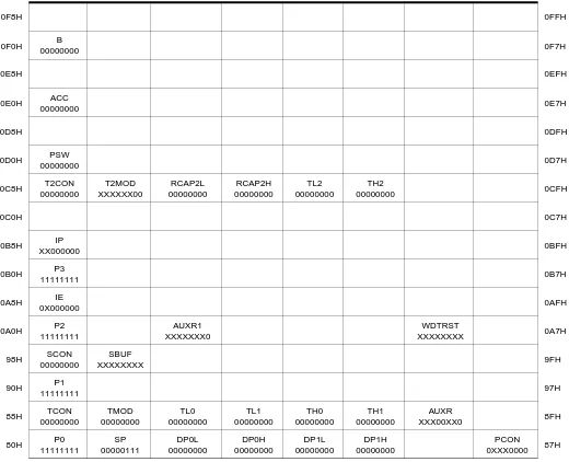
Table 1. AT89S52 SFR Map and Reset Values
AT89S52
6Special Function Registers
A map of the on-chip memory area called the Special Func-tion Register (SFR) space is shown in Table 1.
Note that not all of the addresses are occupied, and unoc-cupied addresses may not be implemented on the chip. Read accesses to these addresses will in general return random data, and write accesses will have an indetermi-nate effect.
User software should not write 1s to these unlisted loca-tions, since they may be used in future products to invoke
new features. In that case, the reset or inactive values of the new bits will always be 0.
Timer 2 Registers: Control and status bits are contained in
registers T2CON (shown in Table 2) and T2MOD (shown in Table 3) for Timer 2. The register pair (RCAP2H, RCAP2L) are the Capture/Reload registers for Timer 2 in 16-bit cap-ture mode or 16-bit auto-reload mode.
Interrupt Registers: The individual interrupt enable bits
[image:31.612.37.582.248.552.2]are in the IE register. Two priorities can be set for each of the six interrupt sources in the IP register.
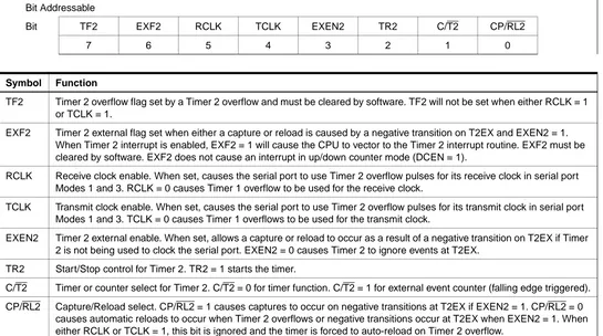
Table 2. T2CON – Timer/Counter 2 Control Register
T2CON Address = 0C8H Reset Value = 0000 0000B
Bit Addressable
Bit TF2 EXF2 RCLK TCLK EXEN2 TR2 C/T2 CP/RL2
7 6 5 4 3 2 1 0
Symbol Function
TF2 Timer 2 overflow flag set by a Timer 2 overflow and must be cleared by software. TF2 will not be set when either RCLK = 1 or TCLK = 1.
EXF2 Timer 2 external flag set when either a capture or reload is caused by a negative transition on T2EX and EXEN2 = 1. When Timer 2 interrupt is enabled, EXF2 = 1 will cause the CPU to vector to the Timer 2 interrupt routine. EXF2 must be cleared by software. EXF2 does not cause an interrupt in up/down counter mode (DCEN = 1).
RCLK Receive clock enable. When set, causes the serial port to use Timer 2 overflow pulses for its receive clock in serial port Modes 1 and 3. RCLK = 0 causes Timer 1 overflow to be used for the receive clock.
TCLK Transmit clock enable. When set, causes the serial port to use Timer 2 overflow pulses for its transmit clock in serial port Modes 1 and 3. TCLK = 0 causes Timer 1 overflows to be used for the transmit clock.
EXEN2 Timer 2 external enable. When set, allows a capture or reload to occur as a result of a negative transition on T2EX if Timer 2 is not being used to clock the serial port. EXEN2 = 0 causes Timer 2 to ignore events at T2EX.
TR2 Start/Stop control for Timer 2. TR2 = 1 starts the timer.
C/T2 Timer or counter select for Timer 2. C/T2 = 0 for timer function. C/T2 = 1 for external event counter (falling edge triggered). CP/RL2 Capture/Reload select. CP/RL2 = 1 causes captures to occur on negative transitions at T2EX if EXEN2 = 1. CP/RL2 = 0
AT89S52
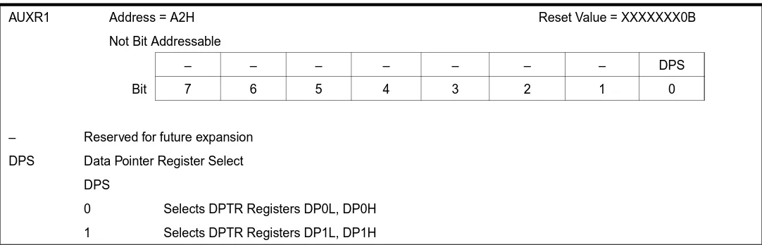
7 Dual Data Pointer Registers: To facilitate accessing both
internal and external data memory, two banks of 16-bit Data Pointer Registers are provided: DP0 at SFR address locations 82H-83H and DP1 at 84H-85H. Bit DPS = 0 in SFR AUXR1 selects DP0 and DPS = 1 selects DP1. The user should always initialize the DPS bit to the
appropriate value before accessing the respective Data Pointer Register.
Power Off Flag: The Power Off Flag (POF) is located at bit
[image:32.612.30.577.90.390.2]4 (PCON.4) in the PCON SFR. POF is set to “1” during power up. It can be set and rest under software control and is not affected by reset.
Table 3a. AUXR: Auxiliary Register
AUXR Address = 8EH Reset Value = XXX00XX0B
Not Bit Addressable
– – – WDIDLE DISRTO – – DISALE
Bit 7 6 5 4 3 2 1 0
– Reserved for future expansion DISALE Disable/Enable ALE
DISALE Operating Mode
0 ALE is emitted at a constant rate of 1/6 the oscillator frequency 1 ALE is active only during a MOVX or MOVC instruction DISRTO Disable/Enable Reset out
DISRTO
0 Reset pin is driven High after WDT times out 1 Reset pin is input only
WDIDLE Disable/Enable WDT in IDLE mode WDIDLE
0 WDT continues to count in IDLE mode 1 WDT halts counting in IDLE mode
Table 3b. AUXR1: Auxiliary Register 1
AUXR1 Address = A2H Reset Value = XXXXXXX0B
Not Bit Addressable
– – – – – – – DPS
Bit 7 6 5 4 3 2 1 0
– Reserved for future expansion DPS Data Pointer Register Select
DPS
[image:32.612.36.577.500.674.2]AT89S52
8Memory Organization
MCS-51 devices have a separate address space for Pro-gram and Data Memory. Up to 64K bytes each of external Program and Data Memory can be addressed.
Program Memory
If the EA pin is connected to GND, all program fetches are directed to external memory.
On the AT89S52, if EA is connected to VCC, program fetches to addresses 0000H through 1FFFH are directed to internal memory and fetches to addresses 2000H through FFFFH are to external memory.
Data Memory
The AT89S52 implements 256 bytes of on-chip RAM. The upper 128 bytes occupy a parallel address space to the Special Function Registers. This means that the upper 128 bytes have the same addresses as the SFR space but are physically separate from SFR space.
When an instruction accesses an internal location above address 7FH, the address mode used in the instruction specifies whether the CPU accesses the upper 128 bytes of RAM or the SFR space. Instructions which use direct addressing access of the SFR space.
For example, the following direct addressing instruction accesses the SFR at location 0A0H (which is P2).
MOV 0A0H, #data
Instructions that use indirect addressing access the upper 128 bytes of RAM. For example, the following indirect addressing instruction, where R0 contains 0A0H, accesses the data byte at address 0A0H, rather than P2 (whose address is 0A0H).
MOV @R0, #data
AT89S52
9
Watchdog Timer
(One-time Enabled with Reset-out)
The WDT is intended as a recovery method in situations where the CPU may be subjected to software upsets. The WDT consists of a 13-bit counter and the Watchdog Timer Reset (WDTRST) SFR. The WDT is defaulted to disable from exiting reset. To enable the WDT, a user must write 01EH and 0E1H in sequence to the WDTRST register (SFR location 0A6H). When the WDT is enabled, it will increment every machine cycle while the oscillator is run-ning. The WDT timeout period is dependent on the external clock frequency. There is no way to disable the WDT except through reset (either hardware reset or WDT over-flow reset). When WDT overover-flows, it will drive an output RESET HIGH pulse at the RST pin.
Using the WDT
To enable the WDT, a user must write 01EH and 0E1H in sequence to the WDTRST register (SFR location 0A6H). When the WDT is enabled, the user needs to service it by writing 01EH and 0E1H to WDTRST to avoid a WDT over-flow. The 13-bit counter overflows when it reaches 8191 (1FFFH), and this will reset the device. When the WDT is enabled, it will increment every machine cycle while the oscillator is running. This means the user must reset the WDT at least every 8191 machine cycles. To reset the WDT the user must write 01EH and 0E1H to WDTRST. WDTRST is a write-only register. The WDT counter cannot be read or written. When WDT overflows, it will generate an output RESET pulse at the RST pin. The RESET pulse duration is 96xTOSC, where TOSC=1/FOSC. To make the best use of the WDT, it should be serviced in those sec-tions of code that will periodically be executed within the time required to prevent a WDT reset.
WDT During Power-down and Idle
In Power-down mode the oscillator stops, which means the WDT also stops. While in Power-down mode, the user does not need to service the WDT. There are two methods of exiting Power-down mode: by a hardware reset or via a level-activated external interrupt which is enabled prior to entering Power-down mode. When Power-down is exited with hardware reset, servicing the WDT should occur as it normally does whenever the AT89S52 is reset. Exiting Power-down with an interrupt is significantly different. The interrupt is held low long enough for the oscillator to stabi-lize. When the interrupt is brought high, the interrupt is serviced. To prevent the WDT from resetting the device while the interrupt pin is held low, the WDT is not started until the interrupt is pulled high. It is suggested that the WDT be reset during the interrupt service for the interrupt used to exit Power-down mode.
To ensure that the WDT does not overflow within a few states of exiting Power-down, it is best to reset the WDT just before entering Power-down mode.
Before going into the IDLE mode, the WDIDLE bit in SFR AUXR is used to determine whether the WDT continues to count if enabled. The WDT keeps counting during IDLE (WDIDLE bit = 0) as the default state. To prevent the WDT from resetting the AT89S52 while in IDLE mode, the user should always set up a timer that will periodically exit IDLE, service the WDT, and reenter IDLE mode.
With WDIDLE bit enabled, the WDT will stop to count in IDLE mode and resumes the count upon exit from IDLE.
UART
The UART in the AT89S52 operates the same way as the UART in the AT89C51 and AT89C52. For further informa-tion on the UART operainforma-tion, refer to the ATMEL Web site (http://www.atmel.com). From the home page, select ‘Prod-ucts’, then ‘8051-Architecture Flash Microcontroller’, then ‘Product Overview’.
Timer 0 and 1
Timer 0 and Timer 1 in the AT89S52 operate the same way as Timer 0 and Timer 1 in the AT89C51 and AT89C52. For further information on the timers’ operation, refer to the ATMEL Web site (http://www.atmel.com). From the home page, select ‘Products’, then ‘8051-Architecture Flash Microcontroller’, then ‘Product Overview’.
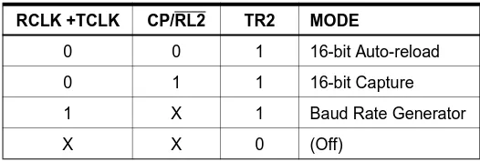
Timer 2
[image:34.612.314.577.609.698.2]Timer 2 is a 16-bit Timer/Counter that can operate as either a timer or an event counter. The type of operation is selected by bit C/T2 in the SFR T2CON (shown in Table 2). Timer 2 has three operating modes: capture, auto-reload (up or down counting), and baud rate generator. The modes are selected by bits in T2CON, as shown in Table 3. Timer 2 consists of two 8-bit registers, TH2 and TL2. In the Timer function, the TL2 register is incremented every machine cycle. Since a machine cycle consists of 12 oscil-lator periods, the count rate is 1/12 of the osciloscil-lator frequency.
Table 3. Timer 2 Operating Modes
RCLK +TCLK CP/RL2 TR2 MODE
0 0 1 16-bit Auto-reload
0 1 1 16-bit Capture
1 X 1 Baud Rate Generator
AT89S52
10In the Counter function, the register is incremented in response to a 1-to-0 transition at its corresponding external input pin, T2. In this function, the external input is sampled during S5P2 of every machine cycle. When the samples show a high in one cycle and a low in the next cycle, the count is incremented. The new count value appears in the register during S3P1 of the cycle following the one in which the transition was detected. Since two machine cycles (24 oscillator periods) are required to recognize a 1-to-0 transi-tion, the maximum count rate is 1/24 of the oscillator fre-quency. To ensure that a given level is sampled at least once before it changes, the level should be held for at least one full machine cycle.
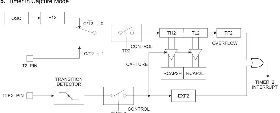
Capture Mode
In the capture mode, two options are selected by bit EXEN2 in T2CON. If EXEN2 = 0, Timer 2 is a 16-bit timer or counter which upon overflow sets bit TF2 in T2CON.
This bit can then be used to generate an interrupt. If EXEN2 = 1, Timer 2 performs the same operation, but a 1-to-0 transition at external input T2EX also causes the current value in TH2 and TL2 to be captured into RCAP2H and RCAP2L, respectively. In addition, the transition at T2EX causes bit EXF2 in T2CON to be set. The EXF2 bit, like TF2, can generate an interrupt. The capture mode is illustrated in Figure 5.
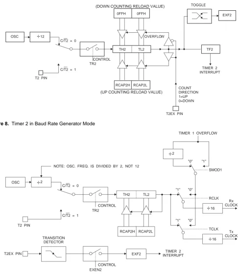
Auto-reload (Up or Down Counter)
[image:35.612.69.544.288.481.2]Timer 2 can be programmed to count up or down when configured in its 16-bit auto-reload mode. This feature is invoked by the DCEN (Down Counter Enable) bit located in the SFR T2MOD (see Table 4). Upon reset, the DCEN bit is set to 0 so that timer 2 will default to count up. When DCEN is set, Timer 2 can count up or down, depending on the value of the T2EX pin.
Figure 5. Timer in Capture Mode
Figure 6 shows Timer 2 automatically counting up when DCEN=0. In this mode, two options are selected by bit EXEN2 in T2CON. If EXEN2 = 0, Timer 2 counts up to 0FFFFH and then sets the TF2 bit upon overflow. The overflow also causes the timer registers to be reloaded with the 16-bit value in RCAP2H and RCAP2L. The values in Timer in Capture ModeRCAP2H and RCAP2L are preset by software. If EXEN2 = 1, a 16-bit reload can be triggered either by an overflow or by a 1-to-0 transition at external input T2EX. This transition also sets the EXF2 bit. Both the TF2 and EXF2 bits can generate an interrupt if enabled. Setting the DCEN bit enables Timer 2 to count up or down, as shown in Figure 6. In this mode, the T2EX pin controls
the direction of the count. A logic 1 at T2EX makes Timer 2 count up. The timer will overflow at 0FFFFH and set the TF2 bit. This overflow also causes the 16-bit value in RCAP2H and RCAP2L to be reloaded into the timer regis-ters, TH2 and TL2, respectively.
A logic 0 at T2EX makes Timer 2 count down. The timer underflows when TH2 and TL2 equal the values stored in RCAP2H and RCAP2L. The underflow sets the TF2 bit and causes 0FFFFH to be reloaded into the timer registers. The EXF2 bit toggles whenever Timer 2 overflows or underflows and can be used as a 17th bit of resolution. In this operating mode, EXF2 does not flag an interrupt.
OSC
EXF2 T2EX PIN
T2 PIN
TR2
EXEN2 C/T2 = 0
C/T2 = 1
CONTROL
CAPTURE
OVERFLOW
CONTROL TRANSITION
DETECTOR TIMER 2
INTERRUPT ÷12
RCAP2L RCAP2H
AT89S52
[image:36.612.62.556.87.319.2]11 Figure 6. Timer 2 Auto Reload Mode (DCEN = 0)
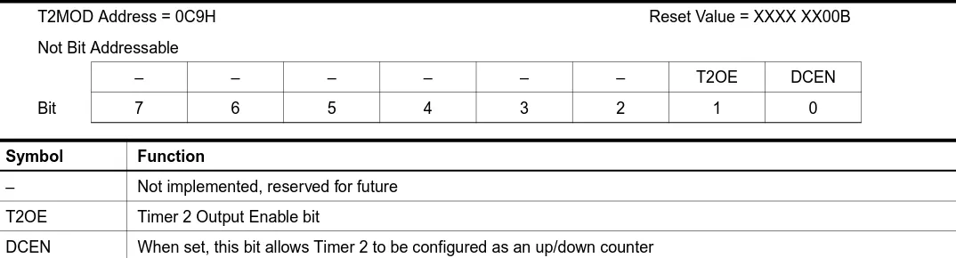
Table 4. T2MOD – Timer 2 Mode Control Register
OSC
EXF2 TF2
T2EX PIN T2 PIN
TR2
EXEN2 C/T2 = 0
C/T2 = 1
CONTR OL
RELO AD
CONTROL TRANSITION
DETECTOR
TIMER 2 INTERRUPT ÷12
RCAP2L RCAP2H
TH2 TL2
OVERFLOW
T2MOD Address = 0C9H Reset Value = XXXX XX00B
Not Bit Addressable
– – – – – – T2OE DCEN
Bit 7 6 5 4 3 2 1 0
Symbol Function
– Not implemented, reserved for future T2OE Timer 2 Output Enable bit
[image:36.612.39.576.335.480.2]AT89S52
12 [image:37.612.72.549.379.633.2]Figure 7. Timer 2 Auto Reload Mode (DCEN = 1)
Figure 8. Timer 2 in Baud Rate Generator Mode
OSC
EXF2
TF2
T2EX PIN COUNT DIRECTION 1=UP 0=DOWN T2 PIN
TR2 CONTROL
OVERFLOW
TOGGLE
TIMER 2 INTERRUPT 12 RCAP2L RCAP2H 0FFH 0FFH TH2 TL2 C/T2 = 0
C/T2 = 1 ÷
(DOWN COUNTING RELOAD VALUE)
(UP COUNTING RELOAD VALUE)
OSC SMOD1 RCLK TCLK Rx CLOCK Tx CLOCK
T2EX PIN T2 PIN
TR2 CONTROL "1" "1" "1" "0" "0" "0"
TIMER 1 OVERFLOW
NOTE: OSC. FREQ. IS DIVIDED BY 2, NOT 12
TIMER 2 INTERRUPT 2 2 16 16 RCAP2L RCAP2H TH2 TL2 C/T2 = 0
C/T2 = 1
AT89S52
13
Baud Rate Generator
Timer 2 is selected as the baud rate generator by setting TCLK and/or RCLK in T2CON (Table 2). Note that the baud rates for transmit and receive can be different if Timer 2 is used for the receiver or transmitter and Timer 1 is used for the other function. Setting RCLK and/or TCLK puts Timer 2 into its baud rate generator mode, as shown in Fig-ure 8.
The baud rate generator mode is similar to the auto-reload mode, in that a rollover in TH2 causes the Timer 2 registers to be reloaded with the 16-bit value in registers RCAP2H and RCAP2L, which are preset by software.
The baud rates in Modes 1 and 3 are determined by Timer 2’s overflow rate according to the following equation.
The Timer can be configured for either timer or counter operation. In most applications, it is configured for timer operation (CP/T2 = 0). The timer operation is different for Timer 2 when it is used as a baud rate generator. Normally, as a timer, it increments every machine cycle (at 1/12 the oscillator frequency). As a baud rate generator, however, it
increments every state time (at 1/2 the oscillator fre-quency). The baud rate formula is given below.
where (RCAP2H, RCAP2L) is the content of RCAP2H and RCAP2L taken as a 16-bit unsigned integer.
Timer 2 as a baud rate generator is shown in Figure 8. This figure is valid only if RCLK or TCLK = 1 in T2CON. Note that a rollover in TH2 does not set TF2 and will not gener-ate an interrupt. Note too, that if EXEN2 is set, a 1-to-0 transition in T2EX will set EXF2 but will not cause a reload from (RCAP2H, RCAP2L) to (TH2, TL2). Thus, when Timer 2 is in use as a baud rate generator, T2EX can be used as an extra external interrupt.
[image:38.612.130.489.442.662.2]Note that when Timer 2 is running (TR2 = 1) as a timer in the baud rate generator mode, TH2 or TL2 should not be read from or written to. Under these conditions, the Timer is incremented every state time, and the results of a read or write may not be accurate. The RCAP2 registers may be read but should not be written to, because a write might overlap a reload and cause write and/or reload errors. The timer should be turned off (clear TR2) before accessing the Timer 2 or RCAP2 registers.
Figure 9. Timer 2 in Clock-Out Mode
Modes 1 and 3 Baud Rates Timer 2 Overflow Rate 16
---=
Modes 1 and 3 Baud Rate
--- Oscillator Frequency
32 x [65536-RCAP2H,RCAP2L)]
---= OSC EXF2 P1.0 (T2) P1.1 (T2EX) TR2 EXEN2
C/T2 BIT
TRANSITION DETECTOR
TIMER 2 INTERRUPT
T2OE (T2MOD.1)
÷2 (8-BITS)TL2
RCAP2L RCAP2H TH2 (8-BITS)
AT89S52
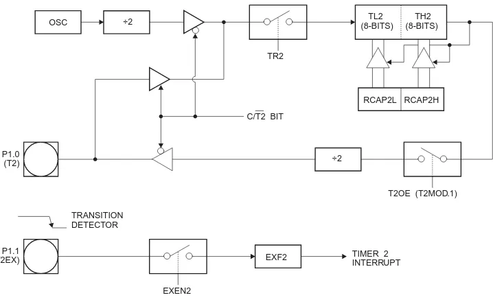
14Programmable Clock Out
A 50% duty cycle clock can be programmed to come out on P1.0, as shown in Figure 9. This pin, besides being a regu-lar I/O pin, has two alternate functions. It can be pro-grammed to input the external clock for Timer/Counter 2 or to output a 50% duty cycle clock ranging from 61 Hz to 4 MHz at a 16 MHz operating frequency.
To configure the Timer/Counter 2 as a clock generator, bit C/T2 (T2CON.1) must be cleared and bit T2OE (T2MOD.1) must be set. Bit TR2 (T2CON.2) starts and stops the timer. The clock-out frequency depends on the oscillator fre-quency and the reload value of Timer 2 capture registers (RCAP2H, RCAP2L), as shown in the following equation.
In the clock-out mode, Timer 2 roll-overs will not generate an interrupt. This behavior is similar to when Timer 2 is used as a baud-rate generator. It is possible to use Timer 2 as a baud-rate generator and a clock generator simulta-neously. Note, however, that the baud-rate and clock-out frequencies cannot be determined independently from one another since they both use RCAP2H and RCAP2L.
Interrupts
The AT89S52 has a total of six interrupt vectors: two exter-nal interrupts (INT0 and INT1), three timer interrupts (Tim-ers 0, 1, and 2), and the serial port interrupt. These interrupts are all shown in Figure 10.
Each of these interrupt sources can be individually enabled or disabled by setting or clearing a bit in Special Function Register IE. IE also contains a global disable bit, EA, which disables all interrupts at once.
Note that Table 5 shows that bit position IE.6 is mented. In the AT89S52, bit position IE.5 is also unimple-mented. User software should not write 1s to these bit positions, since they may be used in future AT89 products. Timer 2 interrupt is generated by the logical OR of bits TF2 and EXF2 in register T2CON. Neither of these flags is cleared by hardware when the service routine is vectored to. In fact, the service routine may have to determine whether it was TF2 or EXF2 that generated the interrupt, and that bit will have to be cleared in software.
[image:39.612.312.578.110.380.2]The Timer 0 and Timer 1 flags, TF0 and TF1, are set at S5P2 of the cycle in which the timers overflow. The values are then polled by the circuitry in the next cycle. However, the Timer 2 flag, TF2, is set at S2P2 and is polled in the same cycle in which the timer overflows.
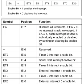
Table 5. Interrupt Enable (IE) Register
Figure 10. Interrupt Sources
Clock-Out Frequency Oscillator Frequency 4 x [65536-(RCAP2H,RCAP2L)]
---=
(MSB) (LSB)
EA – ET2 ES ET1 EX1 ET0 EX0
Enable Bit = 1 enables the interrupt.
Enable Bit = 0 disables the interrupt.
Symbol Position Function
EA IE.7 Disables all interrupts. If EA = 0, no interrupt is acknowledged. If EA = 1, each interrupt source is individually enabled or disabled by setting or clearing its enable bit.
– IE.6 Reserved.
ET2 IE.5 Timer 2 interrupt enable bit. ES IE.4 Serial Port interrupt enable bit. ET1 IE.3 Timer 1 interrupt enable bit. EX1 IE.2 External interrupt 1 enable bit. ET0 IE.1 Timer 0 interrupt enable bit. EX0 IE.0 External interrupt 0 enable bit. User software should never write 1s to unimplemented bits, because they may be used in future AT89 products.
[image:39.612.362.529.441.682.2]AT89S52
15
Oscillator Characteristics
XTAL1 and XTAL2 are the input and output, respectively, of an inverting amplifier that can be configured for use as an on-chip oscillator, as shown in Figure 11. Either a quartz crystal or ceramic resonator may be used. To drive the device from an external clock source, XTAL2 should be left unconnected while XTAL1 is driven, as shown in Figure 12. There are no requirements on the duty cycle of the external clock signal, since the input to the internal clocking circuitry is through a divide-by-two flip-flop, but minimum and maxi-mum voltage high and low time specifications must be observed.
Idle Mode
In idle mode, the CPU puts itself to sleep while all the on-chip peripherals remain active. The mode is invoked by software. The content of the on-chip RAM and all the spe-cial functions registers remain unchanged during this mode. The idle mode can be terminated by any enabled interrupt or by a hardware reset.
Note that when idle mode is terminated by a hardware reset, the device normally resumes program execution from where it left off, up to two machine cycles before the internal reset algorithm takes control. On-chip hardware inhibits access to internal RAM in this event, but access to the port pins is not inhibited. To eliminate the possibility of an unexpected write to a port pin when idle mode is termi-nated by a reset, the instruction following the one that invokes idle mode should not write to a port pin or to exter-nal memory.
Power-down Mode
In the Power-down mode, the oscillator is stopped, and the instruction that invokes Power-down is the last instruction executed. The on-chip RAM and Special Function Regis-ters retain their values until the Power-down mode is termi-nated. Exit from Power-down mode can be initiated either by a hardware reset or by an enabled external interrupt. Reset redefines the SFRs but does not change the on-chip RAM. The reset should not be activated before VCC is restored to its normal operating level and must be held
[image:40.612.337.521.116.285.2]active long enough to allow the oscillator to restart and stabilize.
Figure 11. Oscillator Connections
Note: C1, C2 = 30 pF ± 10 pF for Crystals
[image:40.612.362.524.354.499.2]= 40 pF ± 10 pF for Ceramic Resonators
Figure 12. External Clock Drive Configuration C2
XTAL2
GND XTAL1 C1
XTAL2
XTAL1
GND NC
EXTERNAL OSCILLATOR
SIGNAL
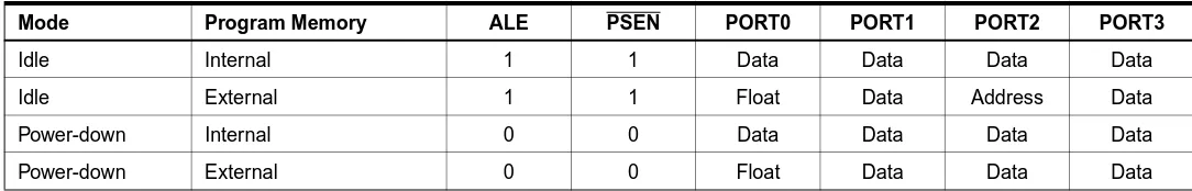
Table 6. Status of External Pins During Idle and Power-down Modes
Mode Program Memory ALE PSEN PORT0 PORT1 PORT2 PORT3
Idle Internal 1 1 Data Data Data Data
Idle External 1 1 Float Data Address Data
Power-down Internal 0 0 Data Data Data Data
[image:40.612.34.576.611.698.2]AT89S52
16Program Memory Lock Bits
The AT89S52 has three lock bits that can be left unpro-grammed (U) or can be prounpro-grammed (P) to obtain the addi-tional features listed in the following table.
When lock bit 1 is programmed, the logic level at the EA pin is sampled and latched during reset. If the device is pow-ered up without a reset, the latch initializes to a random value and holds that value until reset is activated. The latched value of EA must agree with the current logic level at that pin in order for the device to function properly.
Programming the Flash – Parallel Mode
The AT89S52 is shipped with the on-chip Flash memory array ready to be programmed. The programming interface needs a high-voltage (12-volt) program enable signal and is compatible with conventional third-party Flash or EPROM programmers.
The AT89S52 code memory array is programmed byte-by-byte.
Programming Algorithm: Before programming the
AT89S52, the address, data, and control signals should be set up according to the Flash programming mode table and Figures 13 and 14. To program the AT89S52, take the fol-lowing steps:
1. Input the desired memory location on the address lines.
2. Input the appropriate data byte on the data lines. 3. Activate the correct combination of control signals. 4. Raise EA/VPP to 12V.
5. Pulse ALE/PROG once to program a byte in the Flash array or the lock bits. The byte-write cycle is self-timed and typically takes no more than 50 µs.
Repeat steps 1 through 5, changing the address and data for the entire array or until the end of the object file is reached.
Data Polling: The AT89S52 features Data Polling to
indi-cate the end of a byte write cycle. During a write cycle, an attempted read of the last byte written will result in the com-plement of the written data on P0.7. Once the write cycle has been completed, true data is valid on all outputs, and the next cycle may begin. Data Polling may begin any time after a write cycle has been initiated.
Ready/Busy: The progress of byte programming can also
be monitored by the RDY/BSY output signal. P3.0 is pulled low after ALE goes high during programming to indicate BUSY. P3.0 is pulled high again when programming is done to indicate READY.
Program Verify: If lock bits LB1 and LB2 have not been
programmed, the programmed code data can be read back via the address and data lines for verification. The status of the individual lock bits can be verified directly by reading them back.
Reading the Signature Bytes: The signature bytes are
read by the same procedure as a normal verification of locations 000H, 100H, and 200H, except that P3.6 and P3.7 must be pulled to a logic low. The values returned are as follows.
(000H) = 1EH indicates manufactured by Atmel (100H) = 52H indicates 89S52
(200H) = 06H
Chip Erase: In the parallel programming mode, a chip
erase operation is initiated by using the proper combination of control signals and by pulsing ALE/PROG low for a dura-tion of 200 ns - 500 ns.
In the serial programming mode, a chip erase operation is initiated by issuing the Chip Erase instruction. In this mode, chip erase is self-timed and takes about 500 ms.
During chip erase, a serial read from any address location will return 00H at the data output.
Programming the Flash – Serial Mode
The Code memory array can be programmed using the serial ISP interface while RST is pulled to VCC. The serial
interface consists of pins SCK, MOSI (input) and MISO (output). After RST is set high, the Programming Enable instruction needs to be executed first before other opera-tions can be executed. Before a reprogramming sequence can occur, a Chip Erase operation is required.
The Chip Erase operation turns the content of every mem-ory location in the Code array into FFH.
[image:41.612.36.300.138.343.2]Either an external system clock can be supplied at pin XTAL1 or a crystal needs to be connected across pins XTAL1 and XTAL2. The maximum serial clock (SCK)
Table 7. Lock Bit Protection Modes
Program Lock Bits
LB1 LB2 LB3 Protection Type
1 U U U No program lock features 2 P U U MOVC instructions executed
from external program memory are disabled from fetching code bytes from internal memory, EA is sampled and latched on reset, and further programming of the Flash memory is disabled 3 P P U Same as mode 2, but verify is
also disabled
AT89S52
17
frequency should be less than 1/16 of the crystal fre-quency. With a 33 MHz oscillator clock, the maximum SCK frequency is 2 MHz.
Serial Programming Algorithm
To program and verify the AT89S52 in the serial program-ming mode, the following sequence is recommended: 1. Power-up sequence:
Apply power between VCC and GND pins. Set RST pin to “H”.
If a crystal is not connected across pins XTAL1 and XTAL2, apply a 3 MHz to 33 MHz clock to XTAL1 pin and wait for at least 10 milliseconds.
2. Enable serial programming by sending the Pro-gramming Enable serial instruction to pin MOSI/P1.5. The frequency of the shift clock sup-plied at pin SCK/P1.7 needs to be less than the CPU clock at XTAL1 divided by 16.
3. The Code array is programmed one byte at a time by supplying the address and data together with the
appropriate Write instruction. The write cycle is self-timed and typically takes less than 1 ms at 5V. 4. Any memory location can be verified by using the
Read instruction which returns the content at the selected address at serial output MISO/P1.6. 5. At the end of a programming session, RST can be
set low to commence normal device operation. Power-off sequence (if needed):
Set XTAL1 to “L” (if a crystal is not used). Set RST to “L”.
Turn VCC power off.
Data Polling: The Data Polling feature is also available in
the serial mode. In this mode, during a write cycle an attempted read of the last byte written will result in the com-plement of the MSB of the serial output byte on MISO.
Serial Programming Instruction Set
AT89S52
18Programming Interface – Parallel Mode
Every code byte in the Flash array can be programmed by using the appropriate combination of control signals. The write operation cycle is self-timed and once initiated, will automatically time itself to completion.
All major programming vendors offer worldwide support for the Atmel microcontroller series. Please contact your local programming vendor for the appropriate software revision.
[image:43.612.34.575.162.700.2]Notes: 1. Each PROG pulse is 200 ns - 500 ns for Chip Erase. 2. Each PROG pulse is 200 ns - 500 ns for Write Code Data. 3. Each PROG pulse is 200 ns - 500 ns for Write Lock Bits. 4. RDY/BSY signal is output on P3.0 during programming. 5. X = don’t care.
Figure 13. Programming the Flash Memory
[image:43.612.73.548.495.726.2](Parallel Mode)
Figure 14. Verifying the Flash Memory (Parallel Mode) Table 8. Flash Programming Modes
Mode VCC RST PSEN
ALE/ PROG
EA/
VPP P2.6 P2.7 P3.3 P3.6 P3.7
P0.7-0 Data
P2.4-0 P1.7-0
Address
Write Code Data 5V H L
(2)
12V L H H H H DIN A12-8 A7-0
Read Code Data 5V H L H H L L L H H DOUT A12-8 A7-0
Write Lock Bit 1 5V H L
(3)
12V H H H H H X X X
Write Lock Bit 2 5V H L
(3)
12V H H H L L X X X
Write Lock Bit 3 5V H L
(3)
12V H L H H L X X X
Read Lock Bits
1, 2, 3 5V H L H H H H L H L
P0.2, P0.3, P0.4
X X
Chip Erase 5V H L
(1)
12V H L H L L X X X
Read Atmel ID 5V H L H H L L L L L 1EH X 0000 00H
Read Device ID 5V H L H H L L L L L 52H X 0001 00H
Read Device ID 5V H L H H L L L L L 06H X 0010 00H
P1.0-P1.7
P2.6
P3.6 P2.0 - P2.4 A0 - A7
ADDR. 0000H/1FFFH SEE FLASH PROGRAMMING MODES TABLE 3-33 MHz P0 V P2.7 PGM DATA PROG
V /VIH PP
VIH ALE P3.7 XTAL2 EA RST PSEN XTAL1 GND VCC AT89S52 P3.3 P3.0 RDY/ BSY A8 - A12
CC
P1.0-P1.7
P2.6
P3.6 P2.0 - P2.4 A0 - A7
ADDR. 0000H/1FFFH SEE FLASH PROGRAMMING MODES TABLE 3-33 MHz P0 P2.7 PGM DATA (USE 10K PULLUPS) VIH VIH ALE P3.7
XTAL 2 EA
RST PSEN XTAL1 GND VCC AT89S52 P3.3 A8 - A12
AT89S52
[image:44.612.38.582.94.399.2]19 Figure 15. Flash Programming and Verification Waveforms – Parallel Mode
Flash Programming and Verification Characteristics (Parallel Mode)
TA = 20°C to 30°C, VCC = 4.5 to 5.5V
Symbol Parameter Min Max Units
VPP Programming Supply Voltage 11.5 12.5 V
IPP Programming Supply Current 10 mA
ICC VCC Supply Current 30 mA
1/tCLCL Oscillator Frequency 3 33 MHz
tAVGL Address Setup to PROG Low 48tCLCL
tGHAX Address Hold After PROG 48tCLCL
tDVGL Data Setup to PROG Low 48tCLCL
tGHDX Data Hold After PROG 48tCLCL
tEHSH P2.7 (ENABLE) High to VPP 48tCLCL
tSHGL VPP Setup to PROG Low 10 µs
tGHSL VPP Hold After PROG 10 µs
tGLGH PROG Width 0.2 1 µs
tAVQV Address to Data Valid 48tCLCL
tELQV ENABLE Low to Data Valid 48tCLCL
tEHQZ Data Float After ENABLE 0 48tCLCL
tGHBL PROG High to BUSY Low 1.0 µs
tWC Byte Write Cycle Time 50 µs
tGLGH tGHSL
tAVGL
tSHGL
tDVGL
tGHAX
tAVQV
tGHDX
tEHSH
tELQV
tWC
BUSY READY
tGHBL
tEHQZ P1.0 - P1.7
P2.0 - P2.5 P3.4
ALE/PROG PORT 0
LOGIC 1 LOGIC 0
EA/VPP
VPP
P2.7 (ENABLE)
P3.0 (RDY/BSY)
PROGRAMMING ADDRESS
VERIFICATION ADDRESS
AT89S52
20Figure 16. Flash Memory Serial Downloading
Flash Programming and Verification Waveforms – Serial Mode
Figure 17. Serial Programming Waveforms
P1.7/SCK DATA OUTPUT
INSTRUCTION INPUT
CLOCK IN
3-33 MHz
P1.5/MOSI
VIH
XTAL2
RST XTAL1
GND
VCC AT89S52
P1.6/MISO
VCC
[image:45.612.79.542.394.512.2]AT89S52
21
Notes: 1. The signature bytes are not readable in Lock Bit Modes 3 and 4. 2. B1 = 0, B2 = 0 ---> Mode 1, no lock protection
B1 = 0, B2 = 1 ---> Mode 2, lock bit 1 activated B1 = 1, B2 = 0 ---> Mode 3, lock bit 2 activated B1 = 1, B1 = 1 ---> Mode 4, lock bit 3 activated After Reset signal is high, SCK should be low for at least 64 system clocks before it goes high to clock in the enable data bytes. No pulsing of Reset signal is necessary. SCK should be no faster than 1/16 of the system clock at XTAL1.
[image:46.612.36.578.85.465.2]For Page Read/Write, the data always starts from byte 0 to 255. After the command byte and upper address byte are latched, each byte thereafter is treated as data until all 256 bytes are shifted in/out. Then the next instruction will be ready to be decoded.
Table 9. Serial Programming Instruction Set
Instruction
Instruction Format
Operation Byte 1 Byte 2 Byte 3 Byte 4
Programming Enable 1010 1100 0101 0011 xxxx xxxx xxxx xxxx 0110 1001 (Output)
Enable Serial Programming while RST is high
Chip Erase 1010 1100 100x xxxx xxxx xxxx xxxx xxxx Chip Erase Flash memory array
Read Program Memory (Byte Mode)
0010 0000 xxx Read data from Program
memory in the byte mode Write Program Memory
(Byte Mode)
0100 0000 xxx Write data to Program
memory in the byte mode Write Lock Bits(2) 1010 1100 1110 00 xxxx xxxx xxxx xxxx Write Lock bits. See Note (2).
Read Lock Bits 0010 0100 xxxx xxxx xxxx xxxx xx xx Read back current status of the lock bits (a programmed lock bit reads back as a ‘1’) Read Signature Bytes(1) 0010 1000 xxx xxx xxxx Signature Byte Read Signature Byte
Read Program Memory (Page Mode)
0011 0000 xxx Byte 0 Byte 1...
Byte 255
Read data from Program memory in the Page Mode (256 bytes)
Write Program Memory (Page Mode)
0101 0000 xxx Byte 0 Byte 1...
Byte 255
Write data to Program memory in the Page Mode (256 bytes)
D7 D6 D5 D4 D3 D2 D1 D0 A7 A6 A5 A4 A3 A2 A1 A0
A1
2
A11 A10 A9 A8
B2 B1 A1 2 A11 A1 0
A9 A8 A7 A6 A5 A4 A3 A2 A1 A0 D7 D6 D5 D4 D3 D2 D1 D0
LB3 LB2 LB
1
A5 A4 A3 A2 A1 A0
A1
2
A11 A10 A9 A8
A1
2
A11 A10 A9 A8
AT89S52
22 [image:47.612.181.432.119.238.2]Serial Programming Characteristics
Figure 18. Serial Programming Timing
MOSI
MISO
SCK
t
OVSHt
SHSLt
SLSHt
SHOXt
SLIVTable 10. Serial Programming Characteristics, TA = -40°C to 85°C, VCC = 4.0 - 5.5V (Unless otherwise noted)
Symbol Parameter Min Typ Max Units
1/tCLCL Oscillator Frequency 0 33 MHz
tCLCL Oscillator Period 30 ns
tSHSL SCK Pulse Width High 2 tCLCL ns
tSLSH SCK Pulse Width Low 2 tCLCL ns
tOVSH MOSI Setup to SCK High tCLCL ns
tSHOX MOSI Hold after SCK High 2 tCLCL ns
tSLIV SCK Low to MISO Valid 10 16 32 ns
tERASE Chip Erase Instruction Cycle Time 500 ms
[image:47.612.34.584.268.444.2]AT89S52
23
Notes: 1. Under steady state (non-transient) conditions, IOL must be externally limited as follows: Maximum IOL per port pin: 10 mA
Maximum IOL per 8-bit port:
Port 0: 26 mA Ports 1, 2, 3: 15 mA Maximum total IOL for all output pins: 71 mA
If IOL exceeds the test condition, VOL may exceed the related specification. Pins are not guaranteed to sink current greater than the listed test conditions.
2. Minimum VCC for Power-down is 2V.
Absolute Maximum Ratings*
Operating Temperature... -55°C to +125°C *NOTICE: Stresses beyond those listed under “Absolute Maximum Ratings” may cause permanent dam-age to the device. This is a stress rating only and functional operation of the device at these or any other conditions beyond those indicated in the operational sections of this specification is not implied. Exposure to absolute maximum rating conditions for extended periods may affect device reliability.
Storage Temperature ... -65°C to +150°C Voltage on Any Pin
with Respect to Ground ...-1.0V to +7.0V Maximum Operating Voltage ... 6.6V DC Output Current... 15.0 mA
DC Characteristics
The values shown in this table are valid for TA = -40°C to 85°C and VCC = 4.0V to 5.5V, unless otherwise noted.
Symbol Parameter Condition Min Max Units
VIL Input Low Voltage (Except EA) -0.5 0.2 VCC-0.1 V
VIL1 Input Low Voltage (EA) -0.5 0.2 VCC-0.3 V
VIH Input High Voltage (Except XTAL1, RST) 0.2 VCC+0.9 VCC+0.5 V
VIH1 Input High Voltage (XTAL1, RST) 0.7 VCC VCC+0.5 V
VOL Output