© Semiconductor Components Industries, LLC, 2008
December, 2008 − Rev. 1
1 Publication Order Number:
BTA16−600BW3/D
BTA16-600BW3G,
BTA16-800BW3G
Triacs
Silicon Bidirectional Thyristors
Designed for high performance full-wave ac control applications
where high noise immunity and high commutating di/dt are required.
Features
•
Blocking Voltage to 800 V
•
On-State Current Rating of 16 A RMS at 80
°
C
•
Uniform Gate Trigger Currents in Three Quadrants
•
High Immunity to dV/dt
−
1500 V/
m
s minimum at 125
°
C
•
Minimizes Snubber Networks for Protection
•
Industry Standard TO-220AB Package
•
High Commutating dI/dt
−
4.0 A/ms minimum at 125
°
C
•
Internally Isolated (2500 V
RMS)
•
These are Pb
−
Free Devices
MAXIMUM RATINGS (TJ = 25°C unless otherwise noted)
Rating Symbol Value Unit
Peak Repetitive Off−State Voltage (Note 1) (TJ = −40 to 125°C, Sine Wave,
50 to 60 Hz, Gate Open)
BTA16−600BW3G BTA16−800BW3G
VDRM,
VRRM
600 800
V
On-State RMS Current
(Full Cycle Sine Wave, 60 Hz, TC = 80°C)
IT(RMS) 16 A
Peak Non-Repetitive Surge Current (One Full Cycle Sine Wave, 60 Hz, TC = 25°C)
ITSM 170 A
Circuit Fusing Consideration (t = 8.3 ms) I2t 120 A2sec
Non−Repetitive Surge Peak Off−State Voltage (TJ = 25°C, t = 10ms) Peak Gate Power
(Pulse Width ≤1.0 ms, TC = 80°C)
PGM 20 W
Average Gate Power (TJ = 125°C) PG(AV) 1.0 W
Operating Junction Temperature Range TJ −40 to +125 °C Storage Temperature Range Tstg −40 to +150 °C
RMS Isolation Voltage
(t = 300 ms, R.H. ≤ 30%, TA = 25°C)
Viso 2500 V
Stresses exceeding Maximum Ratings may damage the device. Maximum Ratings are stress ratings only. Functional operation above the Recommended Operating Conditions is not implied. Extended exposure to stresses above the Recommended Operating Conditions may affect device reliability.
1. VDRM and VRRM for all types can be applied on a continuous basis. Blocking
voltages shall not be tested with a constant current source such that the voltage ratings of the devices are exceeded.
TRIACS
16 AMPERES RMS
600 thru 800 VOLTS
TO−220AB CASE 221A STYLE 12
http://onsemi.com
BTA16−xBWG AYWW MARKING DIAGRAM
x = 6 or 8
A = Assembly Location Y = Year
WW = Work Week G = Pb−Free Package
Device Package Shipping ORDERING INFORMATION
BTA16−600BW3G TO−220AB (Pb−Free)
Main Terminal 1 Main Terminal 2
4 No Connection
MT1 G MT2
BTA16−800BW3G TO−220AB (Pb−Free)
50 Units / Rail
*For additional information on our Pb−Free strategy and soldering details, please download the ON Semicon-ductor Soldering and Mounting Techniques Reference Manual, SOLDERRM/D.
1 2
BTA16
−
600BW3G, BTA16
−
800BW3G
http://onsemi.com 2
THERMAL CHARACTERISTICS
Characteristic Symbol Value Unit
Thermal Resistance, Junction−to−Case (AC) Junction−to−Ambient
RqJC
RqJA
2.13 60
°C/W
Maximum Lead Temperature for Soldering Purposes 1/8″ from Case for 10 seconds TL 260 °C ELECTRICAL CHARACTERISTICS (TJ = 25°C unless otherwise noted; Electricals apply in both directions)
Characteristic Symbol Min Typ Max Unit
OFF CHARACTERISTICS Peak Repetitive Blocking Current
(VD = Rated VDRM, VRRM; Gate Open) TJ = 25°C Peak On-State Voltage (Note 2)
(ITM = ±22.5 A Peak)
Rate of Change of Commutating Current, See Figure 10. (Gate Open, TJ = 125°C, No Snubber)
(dI/dt)c 4.0 − − A/ms
Critical Rate of Rise of On−State Current
(TJ = 125°C, f = 120 Hz, IG = 2 x IGT, tr ≤100 ns)
dI/dt − − 50 A/ms
Critical Rate of Rise of Off-State Voltage
(VD = 0.66 x VDRM, Exponential Waveform, Gate Open, TJ = 125°C)
dV/dt 1500 − − V/ms
BTA16
−
600BW3G, BTA16
−
800BW3G
VDRM Peak Repetitive Forward Off State Voltage
IDRM Peak Forward Blocking Current
VRRM Peak Repetitive Reverse Off State Voltage IRRM Peak Reverse Blocking Current
Voltage Current Characteristic of Triacs
(Bidirectional Device)
MainTerminal 2 +Quadrant 3
MainTerminal 2 − VTM IH VTM Maximum On State Voltage
IH Holding Current
MT1 (Negative Half Cycle)
MT2 POSITIVE (Positive Half Cycle)
+
Quadrant III Quadrant IV
Quadrant II Quadrant I
Quadrant Definitions for a Triac
IGT − + IGT
All polarities are referenced to MT1.
BTA16
−
600BW3G, BTA16
−
800BW3G
http://onsemi.com 4
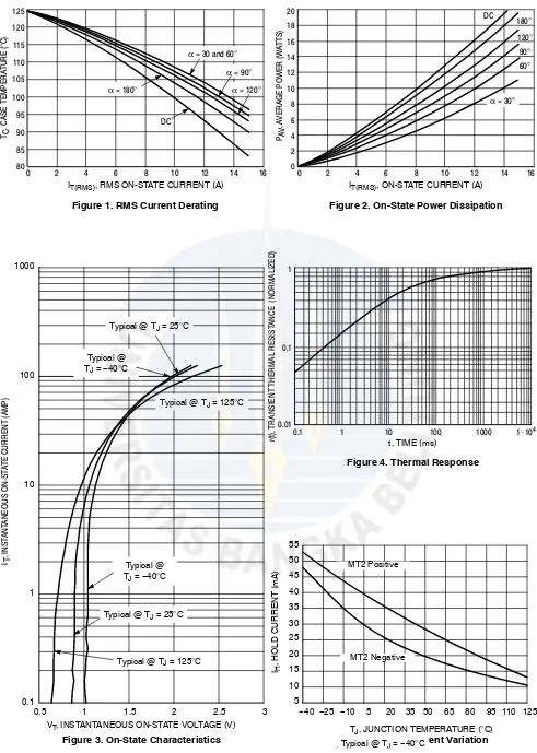
Figure 1. RMS Current Derating IT(RMS), RMS ON-STATE CURRENT (A)
125
Figure 2. On-State Power Dissipation IT(RMS), ON-STATE CURRENT (A)
16
VERAGE POWER (W
A
Figure 3. On-State Characteristics VT, INSTANTANEOUS ON-STATE VOLTAGE (V)
I T
Figure 4. Thermal Response t, TIME (ms)
Figure 5. Hold Current Variation 0.1
, HOLD CURRENT (mA)
BTA16
−
600BW3G, BTA16
−
800BW3G
http://onsemi.com 5
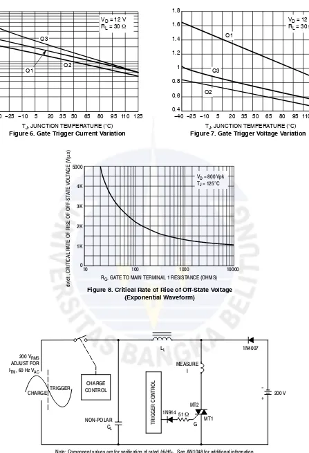
Figure 6. Gate Trigger Current Variation Figure 7. Gate Trigger Voltage Variation
Figure 8. Critical Rate of Rise of Off-State Voltage (Exponential Waveform)
RG, GATE TO MAIN TERMINAL 1 RESISTANCE (OHMS) 5000
TE OF RISE OF OFF‐ST
A
Figure 9. Simplified Test Circuit to Measure the Critical Rate of Rise of Commutating Current (di/dt)c
LL 1N4007
Note: Component values are for verification of rated (di/dt)c. See AN1048 for additional information.
TJ, JUNCTION TEMPERATURE (°C)
TE TRIGGER VOL
BTA16
−
600BW3G, BTA16
−
800BW3G
1. DIMENSIONING AND TOLERANCING PER ANSI Y14.5M, 1982.
2. CONTROLLING DIMENSION: INCH. 3. DIMENSION Z DEFINES A ZONE WHERE ALL
BODY AND LEAD IRREGULARITIES ARE ALLOWED.
DIM MIN MAX MIN MAX MILLIMETERS INCHES
A 0.570 0.620 14.48 15.75
B 0.380 0.405 9.66 10.28
C 0.160 0.190 4.07 4.82
D 0.025 0.035 0.64 0.88
F 0.142 0.147 3.61 3.73
G 0.095 0.105 2.42 2.66
H 0.110 0.155 2.80 3.93
J 0.014 0.022 0.36 0.55
K 0.500 0.562 12.70 14.27
L 0.045 0.060 1.15 1.52
N 0.190 0.210 4.83 5.33
Q 0.100 0.120 2.54 3.04
R 0.080 0.110 2.04 2.79
S 0.045 0.055 1.15 1.39
T 0.235 0.255 5.97 6.47
U 0.000 0.050 0.00 1.27
V 0.045 --- 1.15
---PIN 1. MAIN TERMINAL 1 2. MAIN TERMINAL 2 3. GATE 4. NOT CONNECTED
ON Semiconductor and are registered trademarks of Semiconductor Components Industries, LLC (SCILLC). SCILLC reserves the right to make changes without further notice to any products herein. SCILLC makes no warranty, representation or guarantee regarding the suitability of its products for any particular purpose, nor does SCILLC assume any liability arising out of the application or use of any product or circuit, and specifically disclaims any and all liability, including without limitation special, consequential or incidental damages. “Typical” parameters which may be provided in SCILLC data sheets and/or specifications can and do vary in different applications and actual performance may vary over time. All operating parameters, including “Typicals” must be validated for each customer application by customer’s technical experts. SCILLC does not convey any license under its patent rights nor the rights of others. SCILLC products are not designed, intended, or authorized for use as components in systems intended for surgical implant into the body, or other applications intended to support or sustain life, or for any other application in which the failure of the SCILLC product could create a situation where personal injury or death may occur. Should Buyer purchase or use SCILLC products for any such unintended or unauthorized application, Buyer shall indemnify and hold SCILLC and its officers, employees, subsidiaries, affiliates, and distributors harmless against all claims, costs, damages, and expenses, and reasonable attorney fees arising out of, directly or indirectly, any claim of personal injury or death associated with such unintended or unauthorized use, even if such claim alleges that SCILLC was negligent regarding the design or manufacture of the part. SCILLC is an Equal Opportunity/Affirmative Action Employer. This literature is subject to all applicable copyright laws and is not for resale in any manner.
PUBLICATION ORDERING INFORMATION
N. American Technical Support: 800−282−9855 Toll Free USA/Canada
Europe, Middle East and Africa Technical Support:
Phone: 421 33 790 2910
Japan Customer Focus Center
Phone: 81−3−5773−3850
BTA16−600BW3/D
LITERATURE FULFILLMENT:
Literature Distribution Center for ON Semiconductor P.O. Box 5163, Denver, Colorado 80217 USA
Phone: 303−675−2175 or 800−344−3860 Toll Free USA/Canada
Fax: 303−675−2176 or 800−344−3867Toll Free USA/Canada
Email: [email protected]
HI-SINCERITY
MICROELECTRONICS CORP.
Spec. No. :Preliminary Data Issued Date : 1998.02.01 Revised Date : 1999.08.01 Page No. : 1/2
HSMC Product Specification
DB3
TRIGGER DIODES (Package DO-35)
Description
High reliability glass passivation insuring parameter stability and against contamination.
Absolute Maximum Ratings
(Ta=25
°
C)
•
Maximum Temperatures
Storage Temperature ... -40 ~ +125
°
C
Junction Temperature ... -40 ~ +110
°
C
•
Maximum Power Dissipation
Total Power Dissipation (Ta=25
°
C) ... 150 mW
•
Maximum Voltages and Currents
Breakover Voltage ... 32 V
Breakover Voltage symmetry ...
±
3 V
Repetitive peak on-state Current ... 2 A
Characteristics
(Ta=25
°
C)
Symbol
Min.
Typ.
Max.
Unit
Test Conditions
VBO
28
32
36
V
C=22nF
[ |+VBO| ]-[ |-VBO| ]
-
-
±
3
V
C=22nF
IV±I
5
-
-
V
I=[ IBO to IF=10mA ]
VO
5
-
-
V
IBO
-
-
50
uA
C=22nF
tr
-
1.5
-
uS
IB
-
-
10
uA
VB=0.5 VBO max
HI-SINCERITY
MICROELECTRONICS CORP.
Spec. No. :Preliminary Data Issued Date : 1998.02.01 Revised Date : 1999.08.01 Page No. : 2/2
HSMC Product Specification
DO-35(Glass) Dimension
*:Typical
Inches
Millimeters
Inches
Millimeters
DIM
Min.
Max.
Min.
Max.
DIM
Min.
Max.
Min.
Max.
A
φ
0.0181
φ
0.0220
φ
0.46
φ
0.56
D
0.9646
1.2811
24.50
32.54
B
0.9646
1.2811
24.50
32.54
E
φ
0.0602
φ
0.0787
φ
1.53
φ
2.00
C
0.1200
0.1700
3.05
4.20
Important Notice:
• All rights are reserved. Reproduction in whole or in part is prohibited without the prior written approval of HSMC.
• HSMC reserves the right to make changes to its products without notice.
•HSMC semiconductor products are not warranted to be suitable for use in Life-Support Applications, or systems.
• HSMC assumes no liability for any consequence of customer product design, infringement of patents, or application assistance.
Head Office And Factory :
•Head Office (Hi-Sincerity Microelectronics Corp.) : 10F.,No. 61, Sec. 2, Chung-Shan N. Rd. Taipei Taiwan R.O.C. Tel : 886-2-25212056 Fax : 886-2-25632712, 25368454
•Factory 1 : No. 38, Kuang Fu S. Rd., Fu-Kou Hsin-Chu Industrial Park Hsin-Chu Taiwan. R.O.C Tel : 886-3-5983621~5 Fax : 886-3-5982931
•Factory 2 : No. 17-1, Ta-Tung Rd., Fu-Kou Hsin-Chu Industrial Park Hsin-Chu Taiwan. R.O.C Tel : 886-3-5977061 Fax : 886-3-5979220
B
C
D
A
E
This datasheet has been download from:
www.datasheetcatalog.com
www.vishay.com 31
LCD-016M002B
Vishay
Document Number: 37217 Revision 01-Oct-02
For Technical Questions, Contact: [email protected]
16 x 2 Character LCD
FEATURES
• 5 x 8 dots with cursor
• Built-in controller (KS 0066 or Equivalent)
• + 5V power supply (Also available for + 3V)
• 1/16 duty cycle
• B/L to be driven by pin 1, pin 2 or pin 15, pin 16 or A.K (LED)
• N.V. optional for + 3V power supply
MECHANICAL DATA
ITEM STANDARD VALUE UNIT
Module Dimension 80.0 x 36.0 mm
Viewing Area 66.0 x 16.0 mm
Dot Size 0.56 x 0.66 mm
Character Size 2.96 x 5.56 mm
ABSOLUTE MAXIMUM RATING
ITEM SYMBOL STANDARD VALUE UNIT
MIN. TYP. MAX.
Power Supply VDD-VSS - 0.3 – 7.0 V
Input Voltage VI - 0.3 – VDD V
NOTE: VSS = 0 Volt, VDD = 5.0 Volt
ELECTRICAL SPECIFICATIONS
ITEM SYMBOL CONDITION STANDARD VALUE UNIT
MIN. TYP. MAX.
Input Voltage VDD VDD = + 5V 4.7 5.0 5.3 V
VDD = + 3V 2.7 3.0 5.3 V
Supply Current IDD VDD = 5V – 1.2 3.0 mA
- 20 °C – – –
Recommended LC Driving VDD - V0 0°C 4.2 4.8 5.1 V
Voltage for Normal Temp. 25°C 3.8 4.2 4.6
Version Module 50°C 3.6 4.0 4.4
70°C – – –
LED Forward Voltage VF 25°C – 4.2 4.6 V
LED Forward Current IF 25°C Array – 130 260 mA
Edge – 20 40
EL Power Supply Current IEL Vel = 110VAC:400Hz – – 5.0 mA
Display Position
DD RAM Address
DD RAM Address
DISPLAY CHARACTER ADDRESS CODE:
00 01 0F
40 41 4F
Document Number: 37217
For Technical Questions, Contact: [email protected]
PIN NUMBER SYMBOL FUNCTION
1 Vss GND
2 Vdd + 3V or + 5V
3 Vo Contrast Adjustment
4 RS H/L Register Select Signal
5 R/W H/L Read/Write Signal
6 E H → L Enable Signal
7 DB0 H/L Data Bus Line
8 DB1 H/L Data Bus Line
9 DB2 H/L Data Bus Line
10 DB3 H/L Data Bus Line
11 DB4 H/L Data Bus Line
12 DB5 H/L Data Bus Line
13 DB6 H/L Data Bus Line
14 DB7 H/L Data Bus Line
15 A/Vee + 4.2V for LED/Negative Voltage Output
16 K Power Supply for B/L (OV)