14.2 mm (0.56 inch)
Seven Segment Displays
Technical Data
Features
• Industry Standard Size
• Industry Standard Pinout
15.24 mm (0.6 in.) DIP Leads
on 2.54 mm (0.1 in.) Centers
• Choice of Colors
Red, AlGaAs Red, High
Efficiency Red, Yellow, Green
• Excellent Appearance
Evenly Lighted Segments
Mitered Corners on Segments
Gray Package Gives Optimum
Contrast
±
50
°
Viewing Angle
•
Design Flexibility
Common Anode or Common
Cathode
Single and Dual Digits
Right Hand Decimal Point
±
1. Overflow Character
• Categorized for Luminous
Intensity
Yellow and Green Categorized
for Color
Use of Like Categories Yields a
Uniform Display
• High Light Output
• High Peak Current
• Excellent for Long Digit
String Multiplexing
• Intensity and Color
Selection Option
See Intensity and Color
Selected Displays Data Sheet
• Sunlight Viewable AlGaAs
Description
The 14.2 mm (0.56 inch) LED
seven segment displays are
designed for viewing distances up
to 7 metres (23 feet). These
devices use an industry standard
size package and pinout. Both the
numeric and
±
1 overflow devices
feature a right hand decimal
point. All devices are available as
either common anode or common
cathode.
Red AlGaAs Red HER Yellow Green Package
HDSP- HDSP-[1] HDSP-[1] HDSP- HDSP- Description Drawing
5301 H151 5501 5701 5601 Common Anode Right Hand Decimal A
5303 H153 5503 5703 5603 Common Cathode Right Hand Decimal B
5307 H157 5507 5707 5607 Common Anode ±1. Overflow C
5308 H158 5508 5708 5608 Common Cathode ±1. Overflow D
5321 5521 5721 5621 Two Digit Common Anode Right Hand E
Decimal
5323 5523 5723 5623 Two Digit Common Cathode Right Hand F Decimal
Devices
Note:
1. These displays are recommended for high ambient light operation. Please refer to the HDSP-H10X/K12X AlGaAs and HDSP-555X HER data sheet for low current operation.
HDSP-530X Series
HDSP-532X Series
HDSP-550X Series
HDSP-552X Series
HDSP-560X Series
HDSP-562X Series
HDSP-570X Series
HDSP-572X Series
HDSP-H15X Series
These displays are ideal for most
applications. Pin for pin
equivalent displays are also
available in a low current design.
The low current displays are ideal
FUNCTION
PIN A B C D E F
1 CATHODE e ANODE e CATHODE c ANODE c E CATHODE NO. 1 E ANODE NO. 1 2 CATHODE d ANODE d ANODE c, d CATHODE c, d D CATHODE NO. 1 D ANODE NO. 1 3 ANODE[3] CATHODE[4] CATHODE b ANODE b C CATHODE NO. 1 C ANODE NO. 1
4 CATHODE c ANODE c ANODE a, b, DP CATHODE a, b, DP DP CATHODE NO. 1 DP ANODE NO. 1 5 CATHODE DP ANODE DP CATHOPDE DP ANODE DE E CATHODE NO. 1 E ANODE NO. 2 6 CATHODE b ANODE b CATHODE a ANODE a D CATHODE NO. 2 D ANODE NO. 2 7 CATHODE a ANODE a ANODE a, b, DP CATHODE a, b, DP G CATHODE NO. 2 G ANODE NO. 2 8 ANODE[3] CATHODE[4] ANODE c, d CATHODE c, d C CATHODE NO. 2 C ANODE NO. 2
9 CATHODE f ANODE f CATHODE d ANODE d DP CATHODE NO. 2 DP ANODE NO. 2 10 CATHODE g ANODE g NO PIN NO PIN B CATHODE NO. 2 B ANODE NO. 2 11 A CATHODE NO. 2 A ANODE NO. 2 12 F CATHODE NO. 2 F ANODE NO. 2 13 DIGIT NO. 2 ANODE DIGIT NO. 2 CATHODE 14 DIGIT NO. 1 ANODE DIGIT NO. 1 CATHODE 15 B CATHODE NO. 1 B ANODE NO. 1 16 A CATHODE NO. 1 A ANODE NO. 1 17 G CATHODE NO. 1 G ANODE NO. 1 18 F CATHODE NO. 1 F ANODE NO. 1 NOTES:
1. ALL DIMENSIONS IN MILLIMETRES (INCHES).
2. ALL UNTOLERANCED DIMENSIONS ARE FOR REFERENCE ONLY.
3. REDUNDANT ANODES. 4. REDUNDANT CATHODES.
5. FOR HDSP-5600/-5700 SERIES PRODUCT ONLY.
for portable applications. For
additional information see the
Low Current Seven Segment
Displays data sheet.
Internal Circuit Diagram
Notes:
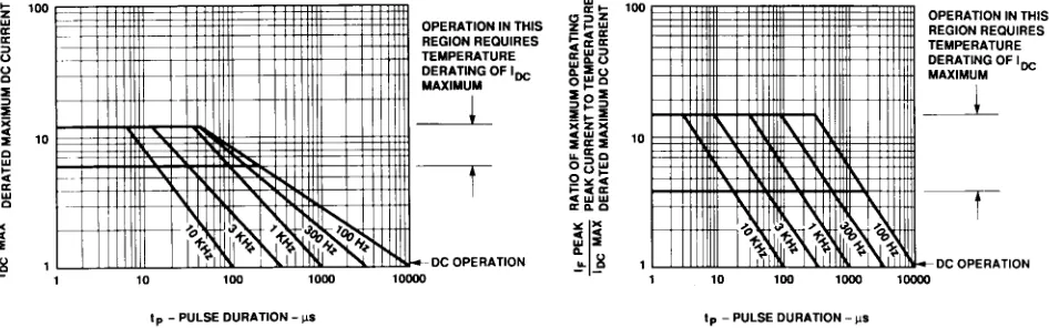
1. See Figure 1 to establish pulsed conditions. 2. Derate above 80°C at 0.63 mA/°C.
3. See Figure 2 to establish pulsed conditions. 4. Derate above 46°C at 0.54 mA/°C.
5. See Figure 7 to establish pulsed conditions. 6. Derate above 53°C at 0.45 mA/°C.
Red AlGaAs Red HER Yellow Green
HDSP-5300 HDSP-H150 HDSP-5500 HDSP-5700 HDSP-5600
Description Series Series Series Series Series Units
Average Power per Segment or DP 82 96 105 80 105 mW
Peak Forward Current per 150[1] 160[3] 90[5] 60[7] 90[9] mA
Segment or DP
DC Forward Current per 25[2] 40[4] 30[6] 20[8] 3010] mA
Segment or DP
Operating Temperature Range -40 to +100 -20 to +100[11] -40 to +100 °C
Storage Temperature Range -55 to +100 °C
Reverse Voltage per 3.0 V
Segment or DP
Lead Solder Temperature for
3 Seconds (1.60 mm [0.063 in.] 260 °C
below seating plane)
Absolute Maximum Ratings
7. See Figure 8 to establish pulsed conditions. 8. Derate above 81°C at 0.52 mA/°C.
9. See Figure 9 to establish pulsed conditions. 10. Derate above 39°C at 0.37 mA/°C.
Electrical/Optical Characteristics at T
A= 25
°
C
Red
Device Series
HDSP- Parameter Symbol Min. Typ. Max. Units Test Conditions
600 1300 IF = 20 mA
Luminous Intensity/Segment[1,2] I
V µcd
(Digit Average) 1400 IF = 100 mA Peak:
1 of 5 df
Forward Voltage/Segment or DP VF 1.6 2.0 V IF = 20 mA
53XX
Peak Wavelength λPEAK 655 nm
Dominant Wavelength[3] λ
d 640 nm
Reverse Voltage/Segment or DP[4] V
R 3.0 12 V IR = 100 µA
Temperature Coefficient of ∆VF/°C -2 mV/°C
VF/Segment or DP
Thermal Resistance LED Junction- RθJ-Pin 345 °C/W/
to-Pin Seg
Device Series
HDSP- Parameter Symbol Min. Typ. Max. Units Test Conditions
Luminous Intensity/Segment[1,2,5] I
V 9.1 16.0 mcd IF = 20 mA
(Digit Average)
1.8 IF = 20 mA
Forward Voltage/Segment or DP VF V
2.0 3.0 IF = 100 mA
H15X
Peak Wavelength λPEAK 645 nm
Dominant Wavelength[3] λ
d 637 nm
Reverse Voltage/Segment or DP[4] V
R 3.0 15 V IR = 100 µA
Temperature Coefficient of ∆VF/°C -2 mV/°C VF/Segment or DP
Thermal Resistance LED Junction- RθJ-Pin 400 °C/W/
to-Pin Seg
Device Series
HDSP- Parameter Symbol Min. Typ. Max. Units Test Conditions
900 2800 IF = 10 mA
Luminous Intensity/Segment[1,2,6] I
V µcd
(Digit Average) 3700 IF = 60 mA Peak:
1 of 6 df
Forward Voltage/Segment or DP VF 2.1 2.5 V IF = 20 mA
55XX
Peak Wavelength λPEAK 635 nm
Dominant Wavelength[3] λ
d 626 nm
Reverse Voltage/Segment or DP[4] V
R 3.0 30 V IR = 100 µA
Temperature Coefficient of ∆VF/°C -2 mV/°C
VF/Segment or DP
Thermal Resistance LED Junction- RθJ-Pin 345 °C/W/
to-Pin Seg
High Efficiency Red
Device Series
HDSP- Parameter Symbol Min. Typ. Max. Units Test Conditions
600 1800 IF = 10 mA
Luminous Intensity/Segment[1,2] I
V µcd
(Digit Average) 2750 IF = 60 mA Peak:
1 of 6 df
Forward Voltage/Segment or DP VF 2.1 2.5 V IF = 20 mA
57XX
Peak Wavelength λPEAK 583 nm
Dominant Wavelength[3,7] λ
d 581.5 586 592.5 nm
Reverse Voltage/Segment or DP[4] V
R 3.0 40 V IR = 100 µA
Temperature Coefficient of ∆VF/°C -2 mV/°C
VF/Segment or DP
Thermal Resistance LED Junction- RθJ-Pin 345 °C/W/
to-Pin Seg
Device Series
HDSP- Parameter Symbol Min. Typ. Max. Units Test Conditions
900 2500 IF = 10 mA
Luminous Intensity/Segment[1,2] I
V µcd
(Digit Average)` 3100 IF = 60 mA Peak:
1 of 6 df
Forward Voltage/Segment or DP VF 2.1 2.5 V IF = 10 mA
56XX
Peak Wavelength λPEAK 566 nm
Dominant Wavelength[3,7] λ
d 571 577 nm
Reverse Voltage/Segment or DP[4] V
R 3.0 50 V IR = 100 µA
Temperature Coefficient of ∆VF/°C -2 mV/°C
VF/Segment or DP
Thermal Resistance LED Junction- RθJ-Pin 345 °C/W/
to-Pin Seg
High Performance Green
Notes:
1. Device case temperature is 25°C prior to the intensity measurement.
2. The digits are categorized for luminous intensity. The intensity category is designated by a letter on the side of the package. 3. The dominant wavelength, λd, is derived from the CIE chromaticity diagram and is that single wavelength which defines the color of
the device.
4. Typical specification for reference only. Do not exceed absolute maximum ratings.
5. For low current operation, the AlGaAs HDSP-H10X series displays are recommended. They are tested at 1 mA dc/segment and are pin for pin compatible with the HDSP-H15X series.
6. For low current operation, the HER HDSP-555X series displays are recommended. They are tested at 2 mA dc/segment and are pin for pin compatible with the HDSP-550X series.
7. The Yellow (HDSP-5700) and Green (HDSP-5600) displays are categorized for dominant wavelength. The category is designated by a number adjacent to the luminous intensity category letter.
Red, AlGaAs Red
Figure 2. Maximum Tolerable Peak Current vs. Pulse Duration – AlGaAs Red.
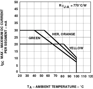
Figure 3. Maximum Allowable DC Current vs. Ambient Temperature.
1.5 0
160
100
80
60
40
20
I – FORWARD CURRENT PER SEGMENT – mAF
RED
AlGaAs RED
2.0
0.5 1.0 2.5 3.0 3.5 4.0
140
120
V – FORWARD VOLTAGE – VF
0
Figure 4. Forward Current vs. Forward Voltage.
HER, Yellow, Green
Figure 7. Maximum Tolerable Peak Current vs. Pulse Duration – HER.
Figure 8. Maximum Tolerable Peak Current vs. Pulse Duration – Yellow.
15 0
2.00
1.25
1.00
0.75
0.50
0.25
RELATIVE LUMINOUS INTENSITY (NORMALIZED TO 1 AT 20 mA)
RED
AlGaAs RED
20
5 10 25 30 35 40
1.75
1.50
I – FORWARD CURRENT PER SEGMENT – mAF
0
Figure 5. Relative Luminous Intensity vs. DC Forward Current.
40 0 5 10 15 20 25 30 35
20 30 40 50 60 70 80 90 100
T – AMBIENT TEMPERATURE – °CA
I MAX – MAXIMUM DC CURRENT
PER SEGMENT – mA
DC
45 50
110 120
R = 770°C/WθJ-A
GREEN YELLOW HER, ORANGE 0 80 50 40 30 20 10
I – FORWARD CURRENT PER SEGMENT – mAF
2.0 3.0 4.0
1.0 70
60
V – FORWARD VOLTAGE – VF
GREEN SERIES YELLOW SERIES HER SERIES
5.0 90
Figure 11. Forward Current vs. Forward Voltage.
Figure 9. Maximum Tolerable Peak Current vs. Pulse Duration – Green.
Figure 10. Maximum Allowable DC Current vs. Ambient Temperature. 15 0 4.0 2.5 2.0 1.5 1.0 0.5 20
5 10 25 30 35 40
3.5
3.0
I – FORWARD CURRENT PER SEGMENT – mAF
0
RELATIVE LUMINOUS INTENSITY (NORMALIZED TO 1 AT 10 mA
HER, YELLOW, GREEN
Figure 12. Relative Luminous Intensity vs. DC Forward Current.
1.1
0
I – PEAK FORWARD CURRENT PER SEGMENT – mA PEAK 0.6 0.8 1.0 1.2 100
10 20 30 40 50 60 70 80 90
1.3 0.9 0.7 1.6 1.5 1.4 GREEN SERIES YELLOW SERIES HER SERIES η
– RELATIVE EFFICIENCY
(NORMALIZED TO 1 AT 10 mA PER SEGMENT)
V
Figure 13. Relative Efficiency
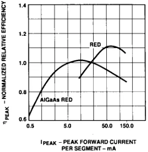
(Luminous Intensity per Unit Current) vs. Peak Current.
Electrical/Optical
For more information on
electrical/optical characteristics,
please see Application Note 1005.
Contrast Enhancement
For information on contrast
enhancement please see
Application Note 1015.
Soldering/Cleaning
Cleaning agents from the ketone
family (acetone, methyl ethyl
ketone, etc.) and from the
chlorinated hydrocarbon family
(methylene chloride, trichloro–
ethylene, carbon tetrachloride,
etc.) are not recommended for
cleaning LED parts. All of these
various solvents attack or dissolve
the encapsulating epoxies used to
form the package of plastic LED