Complex constant number serial multipliers
K.Z. Pekmestzi, P. Kalivas, N. Moshopoulos and J. Sifnaios
Abstract: An efficient implementation of a complex number serial multiplier, when the one factor is constant, is presented. The real and imaginary parts of the constant number are represented in canonic signed digit (CSD) form. The corresponding parts of the non-constant factor are represented in two’s complement form. The real and imaginary parts of the product are obtained in two’s complement form. The CSD representation was chosen because it yields significant hardware reduction. The proposed scheme operates with 100% hardware efficiency; namely, no sign extension words between successive data words are required.
1 Introduction
An operation that is often met in digital signal processing (DSP) algorithms, mainly in fast fourier transform (FFT) computations, is the complex multiplication operation.
The FFT is used in several DSP and communication applications. A representative example is in 3G mobile communications, where the FFT is used for the implemen-tation of the spread spectrum process, where low power dissipation and consequently a small amount of hardware are required.
In high radix FFT calculation, a large number of multiplications use a small number of constant coefficients. These multiplications can be hardwired, resulting in hardware reduction, whereas, for the rest, normal multi-pliers can be used. In addition, the high-speed operation of hardwired multipliers allows the use of serial architectures for further reduction of the power dissipation.
The conventional implementations of complex multipliers are based on the relation
ðAþjBÞðCþjDÞ ¼ACBDþjðADþBCÞ ð1Þ
It requires four multiplications and two additions. Obviously, its implementation requires a significant amount of hardware. A different approach, which considers the complex multiplication as one operation and handles it at the bit-level is presented in [1] for parallel and serial implementations. This results in a significant reduction of the hardware and the circuit layout complexity. Another approach for the parallel implementation of the complex multiplication is given in [2]. The hardware efficiency is improved by combining the computations of the imaginary and real part in the same Wallace tree.
In this paper, a new scheme is proposed for complex multiplication when the one factor is constant. This is the case for the FFT computation where the constant factors are the quantities exp[(2pk/n)j], with k¼0. . .n1. The representation of the real and imaginary parts of the constant coefficient in CSD form[3, 4]is suggested, because
it minimises the required hardware. The other factor is in two’s complement form. A new algorithm for such a complex multiplication is also developed and presented in this paper.
For the implementation of this algorithm the serial/ parallel approach is applied, because it yields more efficient circuits from the aspect of hardware complexity. The disadvantages of this approach are that the resulting circuit is not systolic and operates with 50% efficiency. Therefore, a technique, referred to in [5] and used in [6] for non-constant binary multipliers, is properly modified and used to allow the proposed scheme to operate with 100% efficiency, with negligible hardware and combinational delay overhead.
2 Description of the algorithm
Let us consider the multiplication M¼AX, where X is a complex number X¼Xr+jXi with Xr and Xi in two’s
complement form
Xr¼ xr;n12
n1þX n2
l¼0
xr;l2
l
ð2Þ
Xi¼ xi;n12
n1þXn2 l¼0
xi;l2
l ð
3Þ
andAis the constant complex coefficientA¼Ar+jAiwith ArandAiin CSD form
Ar¼ ar;m12
m1þX m2
k¼0
ar;k2
k
; ar;k¼0;1 ð4Þ
Ai¼ ai;m12
m1þXm2 k¼0
ai;k2
k
; ai;k¼0;1 ð5Þ
Thus, (1) can be written as following
M ¼MrþjMi¼ ðArXrAiXiÞ þjðArXiþAiXrÞ ð6Þ We have four multiplications of constant numbers in CSD form with numbers in two’s complement form. First, an algorithm for such a multiplication is presented. Next, this algorithm is extended for the complex multiplication according to (6).
The authors are with the Department of Electrical and Computer Engineering, National Technical University of Athens, 157 73 Zographou, Athens, Greece
rIEE, 2003
IEE Proceedingsonline no. 20030270 doi:10.1049/ip-cds:20030270
We start from the following relation
whereYis a two’s complement number
Y ¼ yn12n1þ Xn2
l¼0
yl2l ð8Þ
andbis a constant coefficient in CSD form
b¼X From the above equations, it is clear that the partial product Pk is the binary number yyn1yn1 y1y0 for
positivebk, oryn1yyn1 yy1yy0for negativebkplus a ‘1’
at the most significant position. Also, for negativebk, a ‘1’ at
the least significant position must be added. Equation (10) can be written more concisely as follows:
Pk¼ j jbk2n1þY þnk ð11Þ absolute value ofbk. Thus, the final product is
P¼X According to (13), the following constant term Ct is included in the product.
Ct¼ X
For the result to be obtained in two’s complement form, the sum Pm1
i¼0 j jbk2n1þi in (14) must be converted to the same form. Thus, the constant termCtis written as
Ct¼ 2mþn1þX
By extending the above algorithm for the complex multi-plication based on (6), a total constant term is deduced from the corresponding terms of the two added products for the imaginary and real part of the result. This term for the
imaginary partMiis
Cti¼ 2mþnþ respectively and zero otherwise.
By applying the relation 2mþn1þ2n1¼
The corresponding constant term for the real part of the resultMris
3 Circuit implementation
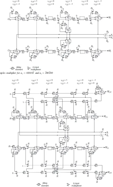
The proposed scheme is based on the serial–parallel multiplier [7]. An example for ar¼010101 and ai¼ 100100 is given in Fig. 1. The data enter the circuit through the two inputsXrandXi. The imaginary and real parts of
the result are obtained from the outputs Mi and Mr
respectively. Two bits, the one fromArand the other from Ai, correspond to each cell. If these bits are both non-zero,
the corresponding cell includes two cascaded full-adders. If only one of these bits is zero, one full-adder is included, which is fed fromXrorXidepending on which of the bits ar,korai,kis non-zero. If bitsar,kandai,kare both zero, no
full-adder is included, and the corresponding cell is empty. The empty cells are also shown in Fig. 2 as dashed boxes. According to (12), the inputs Xr and Xi, for the upper
(imaginary) part of the multiplier, are inverted if the corresponding bitsai,kandar,kare negative. Also, the inputs XrandXiin the lower (real) part are inverted if the bitsar,k
andai,kare negative and positive, respectively. The control
signalR2is activated at the same time with the entrance of
the MSB ofXrandXi, and through the XOR gates inverts
the data inputs. The control signalR1is activated when the
LSB ofXrandXienters the circuit and initialises the carry
and sum delay elements.
Each of the constant termsCtiandCtris incorporated in
The high order parts are
The addition ofCtr,LandCti,Lis performed by initialising
properly with the control signalR1, the carry delay elements
of the full-adders at the first clock cycle of the multi-plication. According to (19) and (20), when the correspond-ing coefficient bits are both zero, the correspondcorrespond-ing bits of Ctr,L and Cti,L are also zero, and no initialisation is
required. When they are both non-zero, the carries of both FA
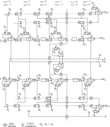
Fig. 2 Complex multiplier forar¼010101andai¼100100operating with 100% efficiency
R2
cascaded full-adders are initialised. The parts CtH can be
added serially from the free sum inputs of the leftmost cell as shown in Fig. 1. Obviously, significant extra hardware is required in this case for storing and shifting these terms.
The above scheme operates with 50% efficiency, because zero words must be inserted between the successive data words that enter the circuit through the linesXrandXi. To
achieve 100% operational efficiency, the following technique[5, 6]is used. When the MSB ofXrandXienters
the circuit, the output of the least significant part of the result ML¼Mr;LþjMi;L is being completed. At the same time, the most significant part MH ¼Mr;HþjMi;H is already stored in carry–save form in the sum and carry delay elements of each full-adder. At the next cycle, the real and imaginary parts are loaded into two double shift registers placed at the lower and upper parts of the multiplier. We name the two shift registers of each double shift register ‘sum’ and ‘carry’ depending on the data they store.
At the same time as the loading, the full-adder rows are starting to be involved in the next multiplication. The content of each double shift register is shifted and added through a serial adder, which converts the most significant part of the results to conventional binary form. Thus, the circuit operates in a pipeline way and 100% operational efficiency is achieved. By applying the above technique in the circuit of Fig. 1 we obtain the scheme shown in Fig. 2. The low order parts of the result are obtained from the outputs Mr,L and Mi,L, and the high order part from the
outputs Mr,Hand Mi,H. The control signal Ris activated
when the LSB of the newXrandXienters the circuit, and
loads the carries and sums of the current multiplication into the double shift registers.
The incorporation ofCtr,L andCti,L is implemented by
initialising the carries of the full-adders. The bits ofCtr,H
andCti,Hare loaded into the carry shift register at the same
time with the sum and carry loading. According to (21), a ‘1’ from Ctr,H andCti,H corresponds to every empty cell,
and a zero to the cells that include one full-adder for the real and imaginary part. A ‘-1’ corresponds to the 4-full-adder cells. For numbers in CSD form, at least a zero digit always exists between non-zero digits. Thus, the adjacent cells of a 4-full-adder cell are always empty cells. In the left adjacent empty cell the corresponding digit ofCtr,HandCti,His ‘1’.
Combining the ‘1’ of this cell with the ‘1’ of the 4-full-adder cell we have a ‘1’ in the 4-full-4-full-adder cell and a zero in the left adjacent cell.
To add the above ‘1’s, we exploit the delay elements of the carry shift registers that are not used for carry loading. Specifically, for every sequence of k empty cells the corresponding delay elements of the carry shift register are not used for loading except the rightmost, where the carryc of the adjacent right non-empty cell is loaded. The k corresponding bits of Cti,H and Ctr,H, which are ‘1’, are
added withcusing the expression
X k1
i¼0
2iþc¼c2kþX
k1
i¼0
cc2i ð22Þ
According to (22), the carry c must be loaded and propagated leftwards through all the cells of the sequence until the first non-empty cell. In every cell, c is loaded inverted except the last cell.
In the 4-full-adder cells, where a ‘1’ fromCti,HandCtr,H
corresponds, the carry that comes from the right adjacent empty cell continues to be propagated leftwards according
to (22). In the left adjacent empty cell, it is added with the carry of the 4-full-adder cell through the half-adder, as shown in Fig. 2. The carry of this half-adder continues to be propagated leftwards.
The terms 2n1inCt
i,HandCtr,Hare added through the
free sum inputs of the leftmost cell when the LSB of X enters the circuit, namely, one clock cycle after the activation ofR. Apparently, if the lengthnofXis greater that the length mof Athis term must be addednm+1 clocks after the activation ofR.In this case, an appropriate number of delay elements must be inserted in the sum inputs of the leftmost cell. Ifnom, then the terms 2n1must be added through the sum input switches of the cell that are located at the (nm)th position from left. The terms 2nþm1are added by entering serially a ‘1’ into the left end
of each carry shift register.
The combinational delay of the above circuit is twice as much as the combinational delay of a simple serial-parallel adder, because of the cascaded full-adders in the 4-full-adder cells. To avoid this, we apply a delay rearrangement
[8–10] based on a graph property, which transform these cells in pipeline form. According to this property, if we consider all the lines that are intersected by a cut across a graph, we can remove one delay element from all the lines that have the same direction and insert a new one into the remaining lines with the opposite direction. The resulting circuit is shown in Fig. 3. The cut in the double cell is also shown in this Figure.
The result of the rearrangement is a delay element to be removed from the sum lines and the double shift registers. A new one is inserted into the linesXr,Xi,R, the sum lines
connecting the cascaded full-adders and the lines that propagate the carry leftwards. The switches that correspond to the removed delay elements are merged with the switches of the next delay elements. The result is that these switches are activated for two clock cycles and consequently the sum and carry loading in the 4-full-adder cells is expanded in two cycles. During the second cycle, the carry of the upper full-adder is loaded into the shift register. This requires an extra clock cycle at the end, namely, a zero bit between the data words.
Another consequence of the above transformation is the decrease of the broadcasting of the lines Xr, Xi and R.
Further reduction of this broadcasting can be achieved by applying the previously mentioned graph property to the empty cells. In this case, six delay elements are removed from sum lines and shift registers and five new are inserted into the linesXr,Xi,Rand the lines that propagate the carry
leftwards. Obviously, this transformation cannot be applied to the right adjacent cell of each 4-full-adder cell, because it increases the combinational delay. The critical path delay of the above scheme is equal to the delay of one XOR gate and one full-adder.
FA
D multiplexer2-input
S
Fig. 3 Final form of the proposed complex multiplier forar¼010101 andai¼100100
Table 1: Comparison of the proposed design with a four multipliers scheme
Multiplication scheme Hardware complexity per coefficient bit (transistors) Efficiency
Four serial/parallel multipliers 2FA+6DE¼96 50%
Proposed scheme 4m 3 FAþ
FA: full-adder (24 transistors); HA: half-adder (10 transistors); DE: dynamic delay element (8 transistors); SW: switch (6 transistors)[11]
Table 2: Hardware complexity for each type of cell of the proposed complex multiplier.
Multiplication scheme No. of cells Hardware complexity
4-full-adder cells m 9
4FA+2HA+11DE+4SW
Untransformed empty cells m 9
6DE+6SW
Transformed empty cells 3m 9
5DE
Cells with twofull-adder 4m 9
2FA+8DE+4SW
Total hardware complexity 4m 3 FAþ
According to Table 1, the proposed design has lower hardware complexity compared to a scheme that consists of four multipliers taking into account that two circuits of the latter are required in order 100% operational efficiency to be achieved. Apparently, a significant part of the hardware efficiency is owed to the CSD representation. The proposed scheme is not fully systolic. A delay element is inserted inX, YandRlines every three cells on average and reduces the broadcasting of these signals.
4 Conclusions
In this paper, a serial complex multiplier for constant factor in CSD form has been presented. An algorithm for the multiplication of a constant number in CSD form with a number in two’s complement form has been introduced. This algorithm significantly reduces the hardware complex-ity. Moreover, the proposed circuit operates with 100% efficiency. The above algorithm can be also applied for the implementation of a parallel complex constant number multiplier. All circuits presented in this paper are extensively verified through simulation.
5 References
1 Pekmestzi, K.Z.: ‘Complex number multipliers’,IEE Proc. E, Comput. Digit. Tech., 1989,136, (1), pp. 70–75
2 Oklobdzija, V.G., Villeger, D., and Soulass, T.: ‘An integrated multiplier for complex numbers’,J. VLSI Signal Process., 1994,7,
pp. 213–221
3 Reitwiesner, G.W.: ‘Binary Arithmetic’, in ‘Advances in computers’ (Academic Press, New York, 1966), Vol. 1, pp. 261–265
4 Peled, A.: ‘On the hardware implementation of digital signal processors’,IEEE Trans. Acoust. Speech Signal Process., 1976, 24, pp. 76–86
5 Dadda, L., and Breveglieri, L.: ‘A modular bit serial convolver’. Proceedings of 3rd IFIP, Wafer scale integration III, (North Holland, Amsterdam, 1990), pp. 279–289
6 Even, G.: ‘Two’s complement pipeline multipliers’,Integr., VLSI J., 1997,22, pp. 23–38
7 Dadda, L.: ‘On serial-input multipliers for two’s complement numbers’,IEEE Trans. Comput., 1989,38, (9), pp. 13411–1345
8 Kung, S.Y.: ‘On supercomputing with systolic/wavefront arrays’,
Proc. IEEE, 1984,72, (7), pp. 867–884
9 Caraiscos, C., and Pekmestzi, K.Z.: ‘Low-latency bit-parallel systolic VLSI implementation of FIR digital filters’, IEEE Trans. Circuits Syst. II, Analog Digit. Signal Process., 1996,43, (7), pp. 529–534
10 Caraiscos, C., and Pekmestzi, K.Z.: ‘A class of systolic bit-serial multipliers’,Int. J. Electron., 1994,76, (3), pp. 463–468