arXiv:1002.0037v2 [cond-mat.mes-hall] 4 Feb 2010
Preprint
Measuring the Temperature of a Mesoscopic Electron System by
means of Single Electron Statistics
Enrico Prati and Matteo Belli
Laboratorio Nazionale Materiali e Dispositivi per la Microelettronica,
Consiglio Nazionale delle Ricerche - Istituto Nazionale per la Fisica della Materia, Via Olivetti 2, I-20041 Agrate Brianza, Italy∗
Marco Fanciulli
Laboratorio Nazionale Materiali e Dispositivi per la Microelettronica,
Consiglio Nazionale delle Ricerche - Istituto Nazionale per la Fisica della Materia, Via Olivetti 2, I-20041 Agrate Brianza, Italy∗ and
Dipartimento di Scienza dei Materiali,
Universita degli Studi Milano-Bicocca, 20125 Milano, Italy
Giorgio Ferrari
Dipartimento di Elettronica e Informazione, Politecnico di Milano, P.za Leonardo da Vinci 32, I-20133 Milano, Italy
Abstract
We measure the temperature of a mesoscopic system consisting of an ultra-dilute two dimen-sional electron gas at the Si/SiO2 interface in a metal-oxide-semiconductor field effect transistor
(MOSFET) by means of the capture and emission of an electron in a point defect close to the interface. Contrarily to previous reports, we show that the capture and emission by point defects in Si n-MOSFETs can be temperature dependent down to 800 mK. As the finite quantum grand canonical ensemble applies, the time domain charge fluctuation in the defect is used to define the temperature of the few electron gas in the channel.
We create a mesoscopic system made of a quantum gas of few electrons in thermal and
particle exchange with a point defect capable of containing one or two electrons, for which
a generalized temperature is determined by virtue of the finite quantum grand partition
ensemble.
Nanoelectronics [1–3] and the study of mesoscopic systems in solid state devices at low
temperature [4] consider ensembles of small numbers of interacting particles. A single donor
atom in a semiconductor [1, 3], defects [5], and quantum dots [6] may contain one or two
localized electrons. These electrons are in thermal contact with a thermal bath consisting
of a two or three dimensional electron system confined in the leads or in a nanometric
channel. There, the total number of electrons may be of the order of tens up to several
hundreds. Temperature is defined by the inverse of the partial derivative of the energy with
respect to the entropy, at a fixed volume [7]. Unlike in macroscopic system, for which the
number of electrons in the reservoir is infinite and conventional statistical physics holds, the
temperature of a mesoscopic system consisting of few electrons confined in a nanostructure
is defined by virtue of a time domain extension of the grand canonical ensemble in the limit
of small finite N [8]. A system constituted by a refrigerated ultra-dilute two dimensional
electron gas at the Si/SiO2 interface in a Metal-Oxide-Semiconductor Field-Effect-Transistor
(MOSFET) and a zero dimensional defect located at the interface realizes an experimental
condition well described by the finite quantum grand canonical ensemble.[8] The point defect
can exchange one electron with the two dimensional system by a thermally assisted tunneling.
Capture and emission of a single electron by defects are monitored by the current
fluctu-actions through the channel of the MOSFET. Such effect goes under the name of Random
Telegraph Signal (RTS) [5, 11–13], because of the peculiar bi-stable current values flowing
randomly as a function of time. In conventional theory of RTS, the same temperature is
attributed to the lattice and to the electrons. [12] The temperature has been previously
extracted from the dependence ofτc/τefrom a static magnetic field in the case of an infinite
thermal bath of electrons in the channel.[13]
We report on the experimental determination of the generalized temperature of a
meso-scopic ensemble of few electrons, for which the generalized temperature is defined by means of
the finite quantum grand canonical ensemble.[8] First, we demonstrate that the detailed
bal-ance principle holds below 10 K by measuring the temperature dependence of the occupancy
[16, 17]. Next, we experimentally determine the generalized temperature of the system
con-stituted by the electrons confined in a defect and the ultra-dilute 2-dimensional electron gas
(2DEG).
The experiment was carried in a n-channel MOS device having a length of 180 nm and
a width of 280 nm, gate oxide thickness of 3.5 nm and a threshold voltage at 4.2 K of
VT= 490 mV.[18] The drain current IDS was measured by a transimpedance amplifier with
bandwidth from dc to about 10 kHz. The electronics is powered by independent batteries
to avoid power-line pick ups and interferences, while the sample was controlled by a 12 bits
data acquisition board. The drain and gate voltages can be set with a resolution better than
50 µV. This setup allowed us to characterize traps with a characteristic time down to 100
µs. The sample was immersed in liquid 3He. We measured the sample at a temperature
below 10 K down to the base temperature of 290 mK. In order to deal with a small number of
identical particles, an electron system confined at the interface between Si and the SiO2 has
been obtained by cooling a MOSFET polarized close to the threshold voltageVT down to the
nominal temperature ofT = 290 mK. The number of electrons in the 2DEG has been roughly
estimated by the charge stored in the MOS capacitor: Q=ǫoxW L/tox(VG−VT), whereW,L
are the width and length of the transistor and tox the oxide thickness. By working few mV
above the threshold voltage, a number of electrons in the order N ≈16 has been obtained.
In confirmation of the low number of electrons, the charge transport at gate voltages close to
the threshold VT exhibits Coulomb blockade characteristics (Figure 1) typical of sequential
tunneling through a few electron quantum dot starting from NQD = 0.[9] The current flows
through an electrostatic island placed between the source and the drain. We observe that
transport is affected by RTS at small bias and close to the threshold. We model the system
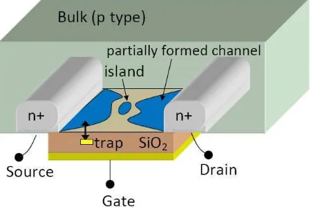
constituted by the quantum dot formed in the channel and the interface defect as depicted
in Figure 2. The defect exchanges one electron with the channel partially formed below the
gate at one side of the electron island. In contrast with previously reported results [16],
the random telegraph signal in the n-MOSFET was found to be temperature dependent
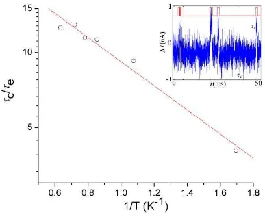
far below 10 K. In Figure 3 the exponential trend of the ratio of the measured emission
time τe and capture time τc is reported between 0.6 K and 1.75 K. The ratio τe/τc depends
exponentially on the inverse of the nominal temperature T. We conclude that the principle
of detailed balance holds in the temperature range considered. The heating of the electron
current is of the order of few nA. This aspect represents the major difference between our
experiment and those reported in the Ref. [16] where the current was of the order of µA.
We measured the effective generalized temperature of the electron gas by studying the B
field dependence of the ratio between the occupancies in the time domain. The trap is a
paramagnetic center with one unpaired electron, capable of capturing and emitting a second
electron (1→2). Such conclusion is provided by the measurement of the characteristic times
τc (capture) and τe (emission) as a function of the gate voltageVG and of the magnetic field
up to 3 T at the nominal temperature of 310 mK.[13] The ratio between the probabilities
of realization of one and two particles occupancy of a mesoscopic system constituted by a
cell in thermal and particle exchange with a few electron gas of N identical particles at the
generalized temperature Θ is described by the Equation
p(1) p(2) = 2e
β(ET+∆EL+∆U−µ(N)(1+23N)) (1)
where β = (kBΘ)−1, µ is the chemical potential, ∆U is the charging energy when two
electrons occupy the point defect, ∆EL is the energy gain of the lattice when the second
electron is captured, and N is the number of electrons of the dilute gas.[8] The expression
Eq. 1 follows from the experimental details of the mechanisms involved in low temperature
RTS. At low temperature the 2DES is weakly coupled with the crystal [10]. Phonons are
involved in the emission and capture of one electron from the defect and the relaxation of
the crystal implies a change of energy of S¯hω where S is the Huang-Rhys factor and ω is
the average phonon frequency in the configuration coordinate picture [14]. We identify the
energy gain of the lattice when an electron is captured with the Huang-Rhys factor ∆EL =
S¯hω. Similarly to the charging energy ∆U of the electrostatic potential of the defect, ∆EL
can be accounted for a negative variation of the electron system Gibbs free energy. Under
the ergodic assumption, the ratio between the average occupation times equals the ratio
between the occupation probabilities, so the experimentally accessible characteristic times
provide information on the statistics via: p(1)/p(2) =τc/τe. The ratioτc/τe experimentally
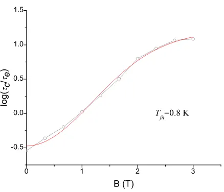
observed as a function of the magnetic field B is reported in Figure 4. The deviation from a
pure exponential trend with respect to theBfield reveals that both the singlet and the triplet
states are accessible at sufficiently high magnetic field.[13] The contribution of the energy
shift from the single electron occupancy to the two electrons occupancy of the point defect
τc/τe is similar to that presented in Ref. [13]:
2 is the average value of the two Zeeman
splittings of the channel and of the trap respectively, δ = E
ergy gap between the singlet and the triplet energy levels in the doubly occupied defect.
The generalized temperature for such system extracted from the fitting is Tf it = 0.80(1)
K. ∆ST=150(5) µeV is due to the different charging energy caused by the different orbital
symmetry of the electron wavefunction for the singlet and the triplet states. The
differ-ence between the generalized electron temperature and the lattice temperature which is in
thermal equilibrium with the 3He at 310 mK is consistent with other reported values in
similar systems. To conclude, we experimentally determined the generalized temperature of
a system of few electrons at cryogenic temperature. We have shown that below 10 K the
capture and the emission of a point defect may be thermally activated and we discussed
the role of phonons. We realized such mesoscopic system in a n-MOSFET, where a point
defect exchanges one electron with the 2DES at the Si/SiO2 interface. The generalized
tem-perature is extracted from the probability of occupation of a mesoscopic system constituted
by a point defect capable of containing either 1 or 2 electrons in thermal contact with a
dilute electron system, in the limit of finite N, with the help of a static magnetic field.
This method provides an estimate of the temperature of a system consisting of a localized
electron in thermal exchange with a small number of electrons confined in two dimensions.
[1] H. Sellier et al., Phys. Rev. Lett.97, 206805 (2006)
[2] G. P. Lansbergen et al., Nature Physics, doi:10.1038/nphys994 (2008) [3] E. Prati et al., Phys. Rev. B80, 165331 (2009)
[4] F. Giazotto et al., Rev. Mod. Phys. 78, 217 (2006) [5] E. Prati et al., J. Appl. Phys., 103, 123707 (2008) [6] M.Sanquer et al., Phys. Rev. B. 61, 7249 (2000)
[8] E. Prati, J. Stat. Mech 1, P01030 (2010)
[9] C. W. J. Beenakker, Phys. Rev. B. 44, 1646 (1991) [10] P. Kivinen et al., J. Appl. Phys. 94, 3, 3201-3205 (2003) [11] K. S. Ralls et al., Phys. Rev. Lett. 52, 228 (1984) [12] A. Palma et al., Phys. Rev. B, 56, 9565 (1997) [13] E. Prati et al., Phys. Rev. B 74, 033309 (2006)
[14] D. Goguenheim et al., J. Appl. Phys. 68, 1059-1069 (1990) [15] R. Hanson et al., Rev. Mod. Phys. 79, 1217 (2007)
[16] J. H. Scofield et al., Appl. Phys. Lett., 76, 22, 3248-3250 (2000) [17] T. M. Bueher, J. Appl. Phys., 96, 11, 6827-6830 (2004)
[18] Courtesy of Dr. Cappelletti and STMicroelectronics
I. FIGURES
Figure 1: The current stability diagram at 300 mK. The energy EG consists of the gate voltage
VG times the coupling constant α= 1.428. The n-MOSFET manifests a quantum dot behaviour,
which reveals the formation of an electron island in the Silicon channel starting from theNQD = 0
Figure 2: Model of a n-MOSFET at cryogenic temperature with a paramegnatic trap close to theSi/SiO2 interface: the current flows by sequential tunelling through the island formed in the
Figure 3: The relative occupation τe/τc versus the inverse of the nominal temperature 1/T. We
demonstrate that in our sample the detailed balance holds down to the nominal value of 600 mK. The sample was operated at VG=495.4 mV and Vd=-9 mV and it carried a current of about 15
0 1 2 3 -0.5
0.0 0.5 1.0 1.5
T
fit
=0.8 K
B (T)
l
o
g
(
c
/
e
)
Figure 4: Magnetic field dependence ofτc/τe. The deviation from a pure exponential trend reveals