An introduction to three-terminal voltage regulators as part of the power system block function earlier in the textbook. Show how a zener diode is used and calculate the various values associated with its operation.
Guided Tour
Learning Features
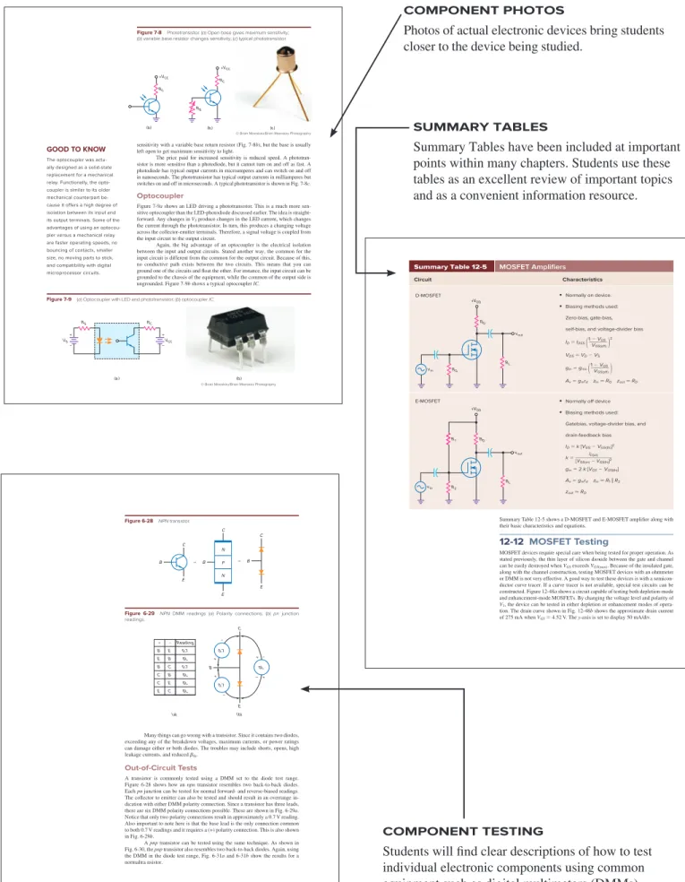
For example, the input circuit may be grounded to the chassis of the equipment, while the common of the output side is ungrounded. A tight voltage source is defined as one whose internal resistance is less than 1⁄100 of the load resistance.
Student
Resources
Instructor Resources
Acknowledgments
Current Edition Reviewers
Although some of the discussion will be reviewed, you will find new ideas, such as circuit approaches, that may make it easier for you to understand semiconductor devices.
Vocabulary
Objectives
Chapter Outline
1-1 The Three Kinds of Formulas
The Defi nition
The Law
GOOD TO KNOW
It says that the force of attraction or repulsion between two charges is directly proportional to the charges and inversely proportional to the square of the distance between them. Through experiments, Coulomb was able to prove that the force was directly proportional to each charge and inversely proportional to the square of the distance between the charges.
The Derivation
Although earlier researchers were able to measure f, Q1, Q2, and d, Coulomb discovered a law that relates the quantities and wrote a formula for it. It says that the charge on a capacitor is equal to its capacitance and the voltage across it.
What to Remember
1-2 Approximations
The Ideal Approximation
When troubleshooting, the ideal approximation is usually sufficient because you are looking for large deviations from normal voltages and currents.
The Second Approximation
The Third Approximation and Beyond
Conclusion
1-3 Voltage Sources
Second Approximation
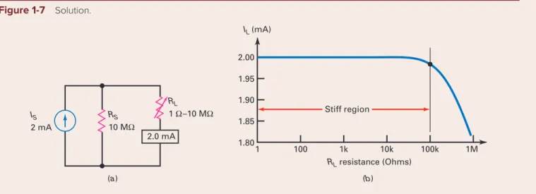
Stiff Voltage Source
1-4 Current Sources
Stiff Current Source
Summary Table 1-1 Properties of Voltage and Current Sources
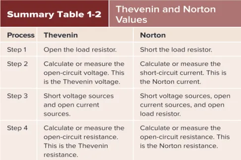
1-5 Thevenin’s Theorem
Defi nition of Thevenin Voltage and Resistance
Application Example 1-3
Opening the load resistor is equivalent to removing it from the circuit, as shown in Fig. Reducing a DC source to zero is equivalent to replacing it with a short circuit, as shown in Fig.
Application Example 1-5
If you want to really appreciate the power of Thevenin's theorem, try calculating the preceding currents using the original circuit in Fig.
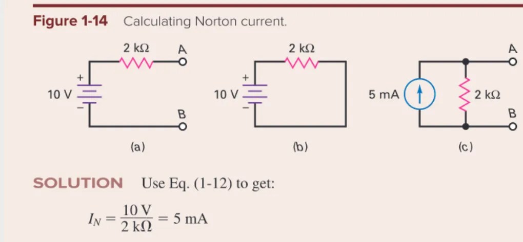
1-6 Norton’s Theorem
Norton resistance is the resistance that an ohmmeter measures across the load terminals when all sources are reduced to zero and the load resistor is open. If you calculate a Thevenin resistor of 10 kV, you immediately know that the Norton resistor is equal to 10 kV.
Basic Idea
If you calculate a Thevenin resistance of 10 kV, you immediately know that the Norton resistance is equal to 10 kV. the original quantities are replaced by double quantities.
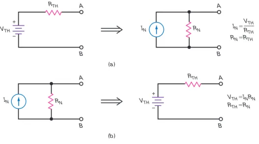
Relationships Between Thevenin and Norton Circuits
1-7 Troubleshooting
An Open Device
A Shorted Device
Procedure
Normal Values
R 1 Open
R 2 Open
Remaining Troubles
Summary
Defi nitions
Derivations
Self-Test
For a solid voltage source to exist, what is the largest internal resistance the source can have. What voltage drops across this internal resistance when the current through it is equal to 2 A.
Problems
Critical Thinking
Troubleshooting
The Multisim troubleshooting files are found in the Instructor Resources section of Connect for Electronic Principles, in a folder called Multisim Troubleshooting Circuits (MTC). For this chapter, the files are labeled MTC01-36 through MTC01-40 and are based on the circuit of Fig.
Multisim Troubleshooting Problems
Take measurements to determine if there is a fault and, if so, determine the circuit fault.
Job Interview Questions
Self-Test Answers
Practice Problem Answers
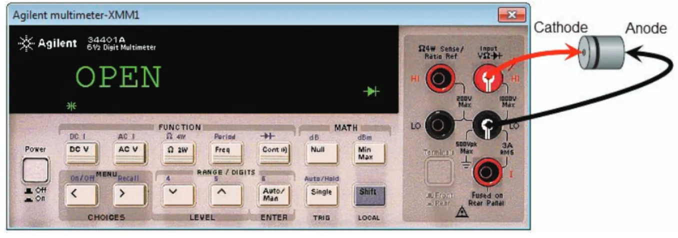
State the two types of carriers and name the type of impurity that causes each to be a majority carrier. Explain the conditions that exist at the pn junction of a forward-biased diode, a forward-biased diode and a reverse-biased diode.
2-1 Conductors
Stable Orbits
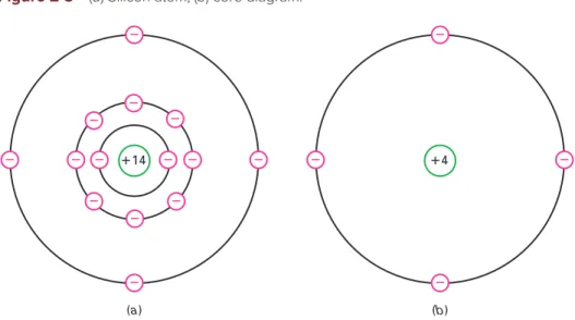
The Core
What is the net charge if an outer electron moves into the valence orbit of Fig. Whenever an atom has an extra electron in its orbital, we call the negatively charged atom a negative ion.
Free Electron
2-2 Semiconductors
Germanium
Silicon
Another common semiconductor element is carbon (C), which is mainly used in the manufacture of resistors. 2-3a, the nucleus has a net charge of 14 because it contains 14 protons in the nucleus and 10 electrons in the first two orbits.
2-3 Silicon Crystals
Covalent Bonds
Valence Saturation
The Hole
Recombination and Lifetime
Main Ideas
A higher temperature increases vibrations at the atomic level, creating more free electrons and holes. But whatever the temperature, a pure silicon crystal has the same number of free electrons and holes.
2-4 Intrinsic Semiconductors
Flow of Free Electrons
Flow of Holes
2-5 Two Types of Flow
2-6 Doping a Semiconductor
Increasing the Free Electrons
Increasing the Number of Holes
If the ambient temperature is 25°C, how many free electrons and holes are there inside the semiconductor. PRACTICE PROBLEM 2-4 As in Example 2-4, if 5 million trivalent atoms are added instead of pentavalent atoms, how many holes are there inside the semiconductor.
Points to Remember
There will be almost no holes in comparison because the only holes in the semiconductor are those produced by heat energy. A trivalent atom is also called an acceptor atom because each hole it contributes can accept a free electron during recombination.
2-7 Two Types of
Extrinsic Semiconductors
2-9 run to the left end of the crystal where they enter the wire and run forward to the positive terminal of the battery.
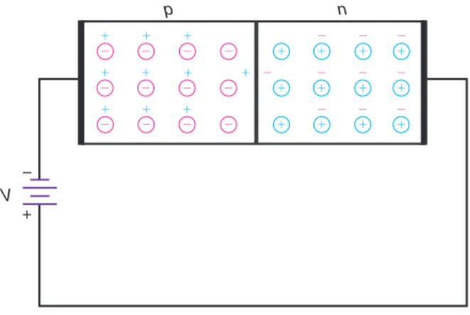
2-8 The Unbiased Diode
The Unbiased Diode
The Depletion Layer
Barrier Potential
2-13a, the electric field between the ions is equivalent to a potential difference called the barrier potential.
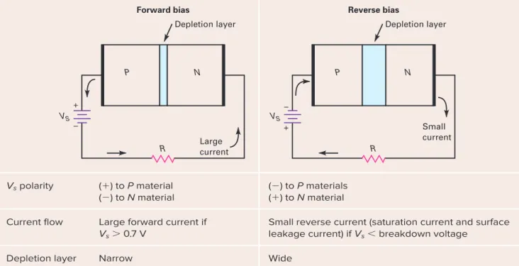
2-9 Forward Bias
The Flow of One Electron
As long as the applied voltage is greater than the barrier potential, there will be a large continuous current in the circuit. In other words, if the source voltage is greater than 0.7 V, a silicon diode allows a continuous current in the forward direction.
2-10 Reverse Bias
Depletion Layer Widens
Minority-Carrier Current
Surface-Leakage Current
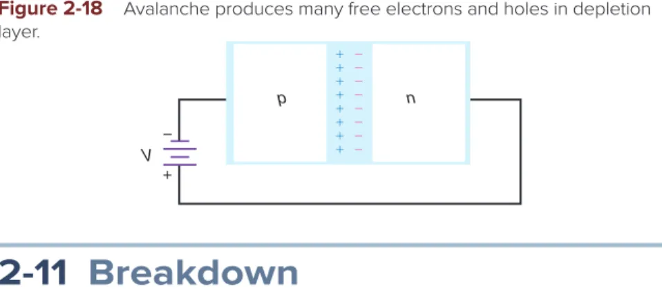
Exceeding the breakdown voltage of a diode does not necessarily mean that you will destroy the diode. As long as the product of reverse voltage and reverse current does not exceed the diode's output, the diode will fully recover.
2-11 Breakdown
2-12 Energy Levels
Higher Energy in Larger Orbit
Summary Table 2-1 Diode Bias
Falling Electrons Radiate Light
Energy Bands
The holes remain in the valence band, but the free electrons go to the next higher energy band, which is called the conduction band. Free electrons move through the conduction band, and holes move through the valence band.
2-13 Barrier Potential and Temperature
2-14 Reverse-Biased Diode
Transient Current
Reverse Saturation Current
Silicon versus Germanium
PRACTICE PROBLEM 2-6 Using the same diode as in Example 2-6, what would be the saturation current at 80°C. If the surface leakage current is 2 nA for a reverse voltage of 25 V, what is the surface leakage current for a reverse voltage of 35 V.
Laws
The energy gap in a silicon atom is the distance between the valence band and the a. If the current is 5 mA through the n-side, what is the current through each of the following.
3-1 Basic Ideas
The Schematic Symbol and Case Styles
Basic Diode Circuit
When the diode is part of a complicated circuit, we can also use Thevenin's theorem to determine if it is forward biased. For example, assume that we have reduced a complicated circuit using Thevenin's theorem to Fig.
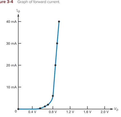
The Forward Region
Knee Voltage
Bulk Resistance
In other words, if the p and n regions were two separate pieces of semiconductor, each would have a resistance that you could measure with an ohmmeter, the same as a regular resistance. The bulk resistance depends on the size of the p and n regions and how heavily doped they are.
Maximum DC Forward Current
Power Dissipation
If the diode voltage is 1.2 V and the diode current is 1.75 A, what is the power dissipation. PRACTICE PROBLEM 3-2 Referring to Example 3-2, what is the diode's power dissipation if the diode voltage is 1.1 V and the diode current is 2 A.
3-2 The Ideal Diode
SOLUTION One way to solve this problem is to devenize the circuit to the left of the diode. If we look back at the source from the diode, we see a voltage divider with 6 kV and 3 kV.
3-3 The Second Approximation
Use the second approximation to calculate the load voltage, load current, and diode power in Fig. 3-8, change the source voltage to 5 V and calculate the new load voltage, current, and diode power.

3-4 The Third Approximation
Application Example 3-7
Application Example 3-8
First, the 1N4001 has a maximum forward current of 1 A and a power rating of 1 W, so the diode is pushed to its limits with a load resistance of 10 V. Second, the load voltage calculated to the third approximation is 9.09 V , which is consistent with the Multisim load voltage (see Fig. 3-12b).
Summary Table 3-1 Diode Approximations
3-5 Troubleshooting
If the diode passes the ohmmeter or DMM test, check the connections because there is nothing else to account for with source voltage but no load voltage. If there is no source voltage, the power supply is defective or a connection between the supply and the diode is open.
3-6 Reading a Data Sheet
Reverse Breakdown Voltage
Maximum Forward Current
Again, a designer considers 1 A to be the absolute maximum rating of the 1N4001, a level of forward current that should not even be approached. In other words, a reliable design will ensure that the forward current is less than 0.5 A under all operating conditions.
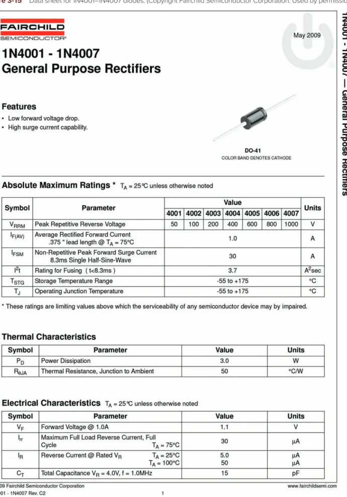
Maximum Reverse Current
3-7 How to Calculate Bulk Resistance
In other words, the more vertical the diode curve is above the knee, the lower the total resistance.
3-8 DC Resistance of a Diode
Reverse Resistance
DC Resistance versus Bulk Resistance
3-9 Load Lines
Equation for the Load Line
An Example
The Q Point
3-10 Surface-Mount Diodes
To determine the diode's internal connections, you can look for data printed on the circuit board, check the schematic diagram, or consult the diode manufacturer's data book. As with many of the small SM devices, you must determine the pin configuration from other data on the circuit board and schematic diagram.
3-11 Introduction to Electronic Systems
If the polarity of the diode is reversed in Figure 3-22a, calculate the load current, load volts. age, load power, diode power and total power. If the polarity of the diode is reversed in Figure 3-22a, calculate the load current, load. voltage, load power, diode power and total power.

Digital/Analog Trainer System
This chapter discusses rectifier circuits, filters, an introduction to voltage regulators, clippers, clamps, and voltage multipliers. 4-1 The half-wave rectifier 4-2 The transformer 4-3 The full-wave rectifier 4-4 The bridge rectifier 4-5 The choke input filter 4-6 The capacitor input filter 4-7 Peak Inverse voltage and.
4-1 The Half-Wave Rectifi er
Ideal Waveforms
To obtain this kind of voltage, we need to filter the half-wave signal (discussed later in this chapter). When troubleshooting, you can use the ideal diode to analyze a half-wave rectifier.
DC Value of Half-Wave Signal
Output Frequency
Higher Approximations
Application Example 4-1
4-2 The Transformer
Phasing Dots
On the positive half cycle of the primary voltage, the secondary winding has a positive half sine wave across it and the diode is forward biased. In the negative half cycle of the primary voltage, the secondary winding has a negative half cycle and the diode is reverse biased.
Turns Ratio
If the secondary point were at the ground end, the secondary voltage would be 180° out of phase with the primary voltage.
4-3 The Full-Wave Rectifi er
DC or Average Value
Application Example 4-3
The full wave rectifier works like two back-to-back half-wave rectifiers.
4-4 The Bridge Rectifi er
Average Value and Output Frequency
Application Example 4-4
As a rule, you will find that the bridge rectifier is used much more than the full wave rectifier. Incidentally, the full-wave rectifier was in use for many years before the bridge rectifier was used.

Second Approximation and Other Losses
For this reason, it has retained the name full-wave rectifier, although the bridge rectifier also has a half-wave output. To distinguish a full-wave rectifier from a bridge rectifier, a half-wave rectifier may be referred to in some literature as a conventional full-wave rectifier, a two-diode full-wave rectifier, or a center-tapped full-wave rectifier. - wave rectifier.
Summary Table 4-1 Unfi ltered Rectifi ers*
Application Example 4-5
4-5 The Choke-Input Filter
When XL is much larger than XC, almost all of the AC voltage falls across the choke. In this example, the choke input filter reduces the AC voltage by a factor of 100.
Filtering the Output of a Rectifi er
In terms of AC voltage, XL is much larger than XC, resulting in a very small AC voltage across the load resistor. This will allow you to see the AC component of the waveform while blocking the DC or average value.
Main Disadvantage
By making RS much smaller than RL, most of the DC component appears across the load resistance. That's how a choke input filter works: almost all of the DC component is passed to the load resistor and almost all of the AC component is blocked.
Switching Regulators
The output of the rectifier has two different components: a dc voltage (average value) and an ac voltage (fluctuating part), as shown in Fig. The only deviation from a perfect dc voltage is the small ac load voltage shown in Fig. .
4-6 The Capacitor-Input Filter
Since it ideally acts as a closed switch, the capacitor is charged and its voltage is equal to the source voltage at each instant of the first quarter cycle. Ideally, all the capacitor input filter does is charge the capacitor to the peak voltage during the first quarter cycle.
Eff ect of Load Resistor
Full-Wave Filtering
Therefore, the peak-to-peak ripple is half the size it would be with a half-wave rectifier.
The Ripple Formula
If you use an AC voltmeter to measure the wave, you can convert the peak to peak value given by Eq. 4. Dividing by 2 converts the peak-to-peak value to a peak value, and dividing by Ï—2 gives the rms value of a sine wave with the same peak-to-peak value as the ripple voltage.
Exact DC Load Voltage
Because of the 0.7 V across the conducting diode, the actual dc load voltage will be closer to 16 V than 17 V. Because of the 1.4 V across the two conducting diodes and the ripple, the actual dc load voltage will be closer to 32 V. than in 34 V.

Application Example 4-9
4-7 Peak Inverse Voltage and Surge Current
Half-Wave Rectifi er with Capacitor-Input Filter
As long as the breakdown voltage of the diode is greater than this, the diode will not be damaged.
Full-Wave Rectifi er with Capacitor-Input Filter
Bridge Rectifi er with Capacitor-Input Filter
Surge Resistor
The 1N4001 is more than sufficient, as the peak inverse voltage is much lower than the breakdown voltage of 50 V.
4-8 Other Power-Supply Topics
Commercial Transformers
This is an approximation because the calculated turns ratio decreases as the load current decreases.
Calculating Fuse Current
Slow-Blow Fuses
Calculating Diode Current
Reading a Data Sheet
Summary Table 4-2 Capacitor-Input Filtered Rectifi ers*
RC Filters
LC Filter
For low-voltage power supplies, the LC filter has been replaced by an integrated circuit (IC). Because of their low cost, IC voltage regulators are now the standard method used to reduce ripple.
4-9 Troubleshooting
It is now becoming obsolete in typical power supplies due to the size and cost of inductors. A voltage regulator IC, one type of integrated circuit, is between the filter capacitor and the load resistor.
Summary Table 4-3 Power Supply Block Diagram
The dc voltage drop across inductors is much less than it is across resistors of RC sections because the winding resistance is less. Second, if there is dc load voltage but it is lower than it should be, look at the dc load voltage with an oscilloscope and measure the ripple.
Common Troubles
Summary Table 4-4 Typical Troubles for Capacitor-Input Filtered Bridge Rectifi er
4-10 Clippers and Limiters
Small-Signal Diodes
The Positive Clipper
Defi ning Conditions
Solid cutter: 100RB⬍ RS⬍ 0.01RL (4-17) This means that the series resistance must be 100 times greater than the mass resistance and 100 times less than the load resistance. For example, if the diode has a large resistance of 30 V, the series resistance should be at least 3 kV and the load resistance should be at least 300 kV.
The Negative Clipper
The Limiter or Diode Clamp
The diodes conduct only when something is abnormal, when the signal is too large.
Biased Clippers
Combination Clipper
Variations
4-11 Clampers
Positive Clamper
After the first quarter cycle, the output voltage is a positively clamped sine wave with a zero reference level; that is, it drops to a level of 0 V. Therefore, the clamping is not perfect, and the negative peaks have a reference level of 20.7 V.
Negative Clamper
For example, television receivers use clamps to change the reference level of video signals. Then you will see how easy it is to eliminate the problem of potential obstruction.
Peak-to-Peak Detector
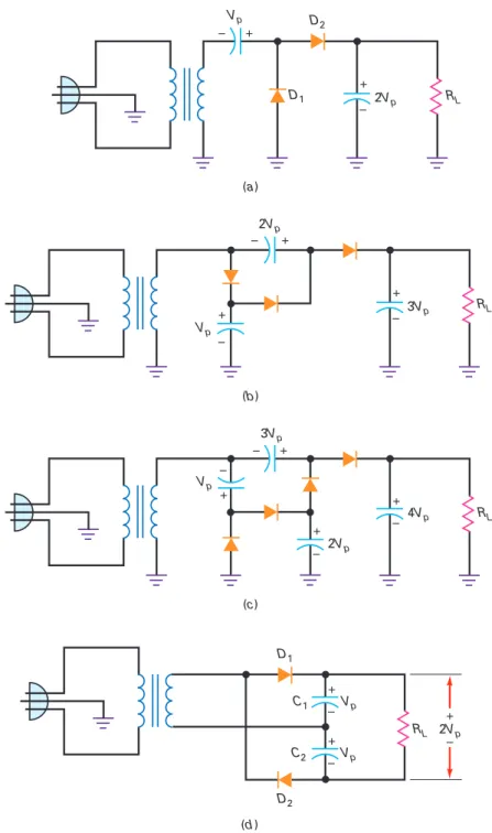
4-12 Voltage Multipliers
Voltage Doubler
Voltage Tripler
Voltage Quadrupler
Full-Wave Voltage Doubler
What is the peak load voltage in a full wave rectifier if the secondary voltage is 20 Vrms. What is the peak load voltage from a bridge rectifier for a secondary voltage of 12.6 Vrms.
5-1 The Zener Diode
V Graph
Zener Resistance
Similarly, in the breakdown region, the reverse voltage across the diode is equal to the breakdown voltage plus the additional voltage across the common resistor. In the inverted region, the bulk resistance is called the Zener resistance.
Zener Regulator
5-1c, the zener resistor means that an increase in reverse current produces a small increase in reverse voltage. This small increase may be important in design work, but not in troubleshooting and preliminary analysis.
Ohm’s Law Again
When you have a series current value, you also have a zener current value.
Ideal Zener Diode
5-2 The Loaded Zener Regulator
Breakdown Operation
Series Current
Load Current
Zener Current
Zener Eff ect
Since this Thevenin voltage is greater than the Zener voltage, the Zener diode operates in the breakdown region.
Temperature Coeffi cients
Application Example 5-4
Application Example 5-5
Application Example 5-6
5-3 Second Approximation of a Zener Diode
Eff ect on Load Voltage
Eff ect on Ripple
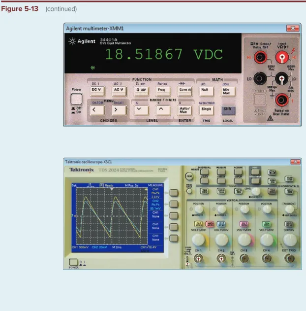
Application Example 5-9
Since the ripple is large, the voltage across the capacitor swings from a high of 19.8 V to a low of 17.1 V. If you average these two values, you get 18.5 V as the approximate DC voltage across the filter capacitor.
5-4 Zener Drop-Out Point
Worst-Case Conditions
PRACTICE PROBLEM 5-10 Using Example 5-10, what is the maximum allowable series resistance if the regulated output voltage is 15 V. If the series resistance is less than 410 V, the zener regulator will operate correctly under all conditions.
5-5 Reading a Data Sheet
Maximum Power
Maximum Current
Tolerance
As long as the zener current is beyond the knee of the curve, you can use 8.0 V as an approximate value of the zener resistor. The data sheet contains a lot of additional information, but it is mainly aimed at designers.
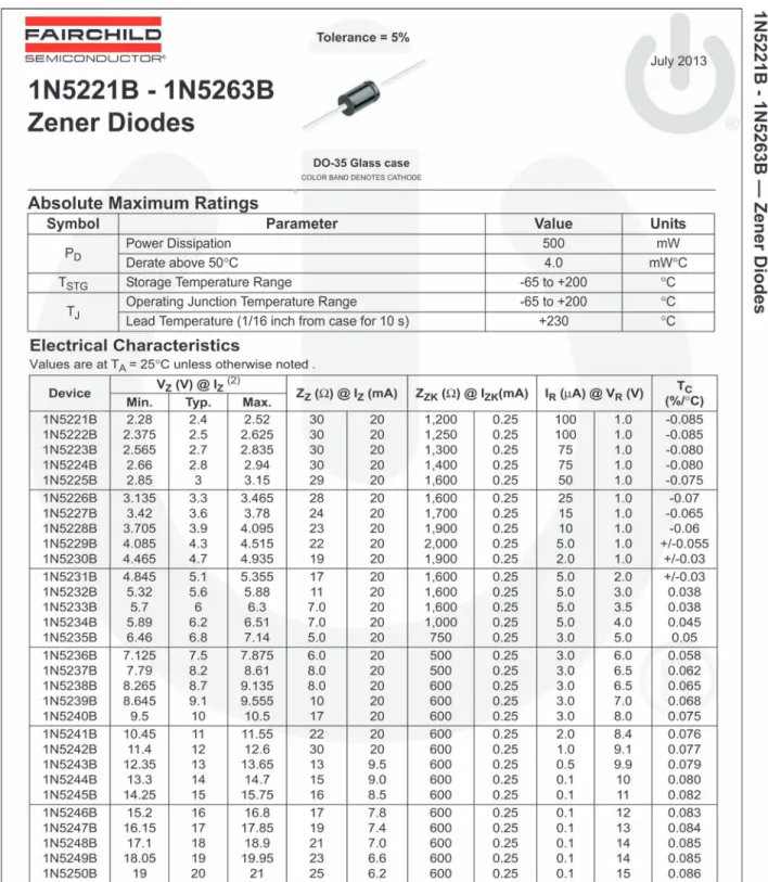
Derating
If you are involved in the design, you should carefully read the data sheet, including the notes that specify how the quantities were measured.
5-6 Troubleshooting
Unique Symptoms
Ambiguous Symptoms
At this point, the troubleshooter will disconnect the series resistor and measure its resistance with an ohmmeter. Therefore, you must include what-if questions in the form of short-circuited components as well as open-ended components.
Other ways to get a short include a solder splash between traces on a circuit board, a solder ball touching two traces, and so on. In other words, use a very small resistance for a short and a very large resistance for an open resistance.
Troubles and Symptoms
When calculating the voltages, remember this: A shorted component corresponds to a resistance of zero, and an open component corresponds to a resistance of infinity.
For example, a shorted RS will destroy the zener diode and may also open the load resistor. However, this test will not show whether the zener diode has the appropriate breakdown voltage VZ.
5-7 Load Lines
5-8 Light-Emitting Diodes (LEDs)
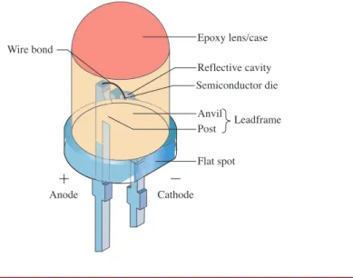
Light-Emitting Diode
The voltage drop should be close to its nominal value. the cathode side of the LED. The color of the light, which corresponds to the wavelength energy of the photons, is largely determined by the energy band gap of the semiconductor materials used.
LED Voltage and Current
LED Brightness
LED Specifi cations and Characteristics
Application Example 5-12
Application Example 5-13
Application Example 5-14
Application Example 5-15
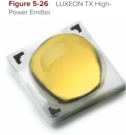
High-Power LEDs
Application Example 5-16
The luminous efficiency of a source is the ratio of output luminous flux (lm) to electrical power (W) given in lm/W. For comparison, the luminous efficacy of a typical incandescent lamp is 16 lm/W and a compact fluorescent lamp has a typical rating of 60 lm/W.
5-9 Other Optoelectronic Devices
Seven-Segment Display
Optocoupler
Laser Diode
New applications are being found as the lasing wavelength is pushed lower into the visible spectrum with visible laser diodes (VLDs). Also, near-infrared diodes are being used in car vision systems, sensors and security systems.
5-10 The Schottky Diode
Charge Storage
Charge Storage Produces Reverse Current
Until the stored charges pass through the intersection or come together again, the countercurrent flow will continue.
Reverse Recovery Time
Poor Rectifi cation at High Frequencies
Eliminating Charge Storage
Hot-Carrier Diode
High-Speed Turnoff
Applications
Because a Schottky diode has a barrier potential of only 0.25 V, you occasionally see it used in low-voltage bridge rectifiers because you subtract only 0.25 V for each diode instead of the usual 0.7 V when using the second approximation.
5-11 The Varactor
Equivalent Circuit and Symbol
Capacitance Decreases at Higher Reverse Voltages
Varactor Characteristics
CR is the ratio of Ct measured at 3 Vdc divided by Ct measured at 25 Vdc.
5-12 Other Diodes
Varistors
Application Example 5-17
One of the devices used for line filtering is the varistor (also called a transient suppressor).
Current-Regulator Diodes
Step-Recovery Diodes
(c) snap-off produces a positive voltage step rich in harmonics. a) Breakdown occurs at 20.1 V; (b) circuit that corrects weak AC signal. step recovery diode is also known as a snap diode. Because of this, step recovery diodes are useful in frequency multipliers, circuits whose output frequency is a multiple of the input frequency.
Back Diodes
The sudden step in current is rich in harmonics and can be filtered to produce a sine wave with a higher frequency.
Tunnel Diodes
Because of this, step recovery diodes are useful in frequency multipliers, circuits whose output frequency is a multiple of the input frequency. a) Construction; (b) schematic symbol;. Step-recovery diode Clips off during reverse conduction Frequency multipliers Back diode Conducts better in reverse Weak-signal rectifiers Tunnel diode Has a negative-resistance region High-frequency oscillators.
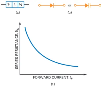
PIN Diodes