Hall mobility as a function of Hall carrier density.. modeled with and without the Σ-band contribution. Transport properties of Cl-doped PbS as a function of temperature: a) resistivity, .. b) Seebeck coefficient, c) Hall carrier density, d) Hall mobility.
Introduction
- Thermoelectric Effects
- Devices and Thermoelectric Materials
- IV-VI compounds
- Summary of Research
It is clear from equation 1.1 that the maximum conversion efficiency is determined by the value zT of the material. When this is taken into account, the transport behavior of the alloys can again be accurately predicted.
Experimental Methods
- synthesis
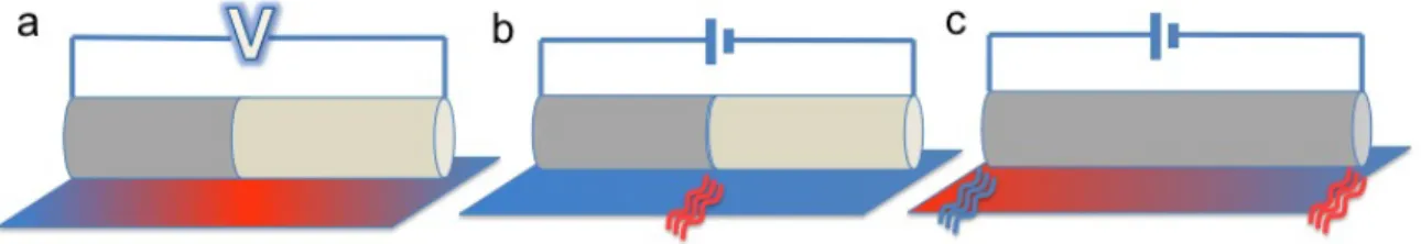
- Seebeck Coefficient Measurement
- Hall and Resistivity Measurements
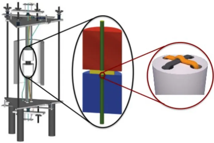
- Thermal Conductivity Measurement
On the other hand, the magnetic field in the center of the coil (where the samples are) is very weak (not more than 200 Gauss rated with a coil diameter of 100 mm and a current of 250 A). In fact, it is necessary to compare the measured values with those from theory, i.e., the Dulong-Petit Cv value, 3kB/atom, when it is above the Debye temperature (as opposed to the Debye integral) plus the volume expansion correction term72 9α2T /βd, α. is the linear coefficient of thermal expansion, β is the isothermal compressibility, and d is the density.
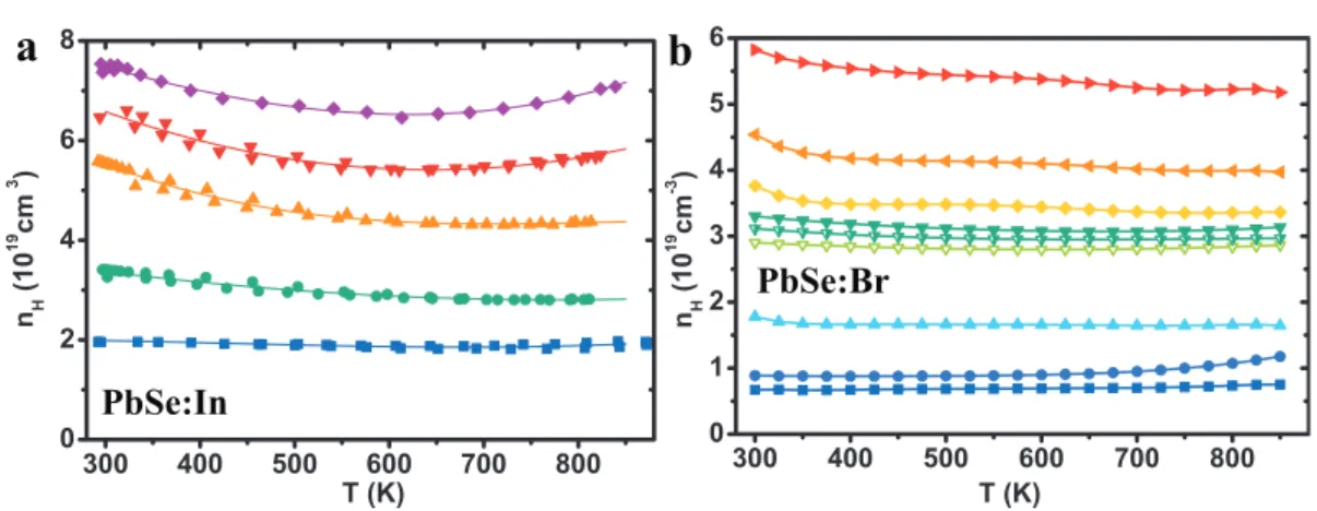
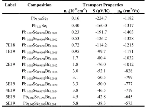
N-type PbSe Doped on Anion Site
Introduction
Sample Synthesis and Properties
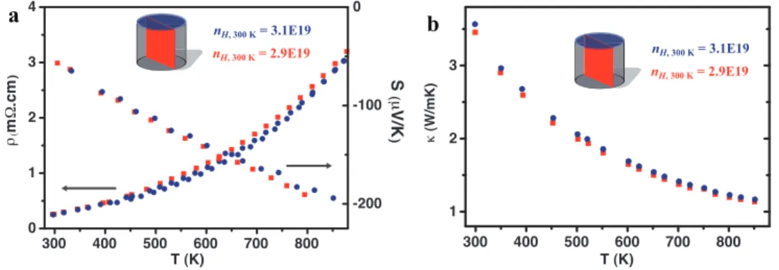
The very similar carrier density and transport properties shown in Figure 3.5 indicate good homogeneity of the hot pressed samples. D by Androulakis76 (Northwestern high doping), sample C by Androulakis76 (Northwestern low doping), sample 1 by Alekseeva77 (Ioffe Institute low doping), and two slices of "Br0.0018" samples from this study (Caltech high doping 3.1E19 and 2.9E19).. The legends in c) represent: sample 1 by Alekseeva77 (Ioffe Institute, n), sample 7 by Alekseeva77 (Ioffe Institute, p), sample C by Androulakis76 (Northwestern, n, low doping), sample D by Androulakis76 (Northwestern, n, high doping, solid triangles), sample “PbSe- In 3E19 electron⁄cm3 ” by Androulakis78 (Northwestern, n, high doping, open triangles filled with dots), sample “x = 0.01” by Wang79 (Wuhan ) Univ.
Transport Properties Modeling
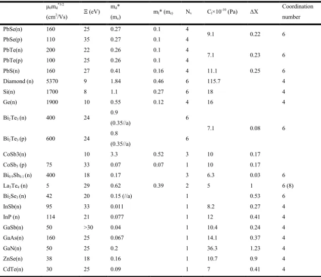
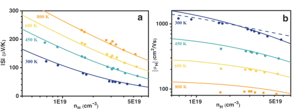
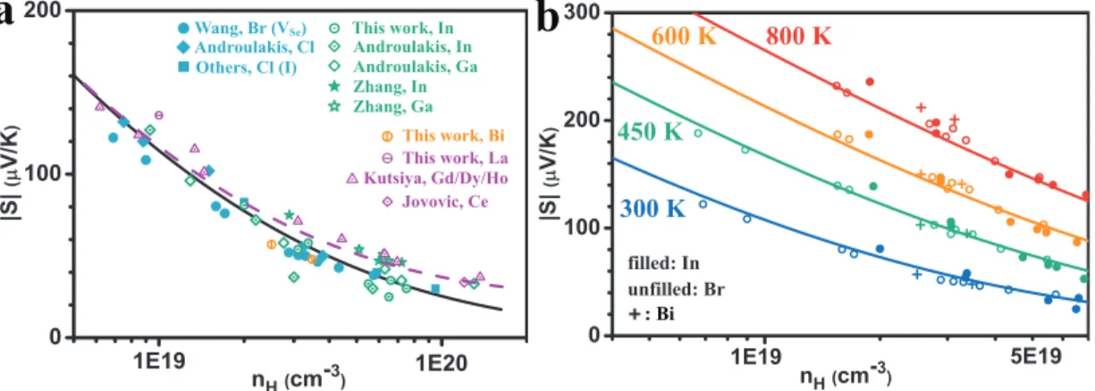
The density of states effective mass, m* = NV2/3mb*, can be easily determined from the dependence of the carrier density on the Seebeck coefficient (called the Pisarenko relation) and is found to be in the range of me. Carrier density dependence of a) Seebeck coefficient and b) Hall mobility of Br-doped PbSe at different temperatures.
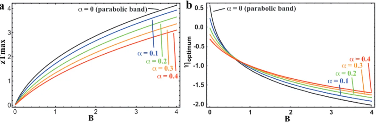
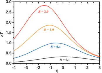
Thermoelectric Quality Factor B
If we rewrite B (or β) under the acoustic phonon scattering assumption, which we call the quality factor, since B is the combination of material properties of a semiconductor that directly relates to the maximum material performance, zT, when the carrier concentration is optimized. Where Nv is the degeneration of the valley and mI* is the effective inertial mass defined later in equation 3.15.
Band Models and Transport Properties Equations for Single Band
An important result of the interaction (kp perturbation theory) is that the effective mass of carriers in a Kane band depends on both the band gap and its energy: m0. Reducing the tire gap of a Kane tire system could potentially increase the maximum zT due to reduced effective tire mass.
Acoustic Phonon Scattering and Deformation Potential
Such a process is called the deformation potential scattering of acoustic phonons, or more generally, acoustic phonon scattering for short (Figure 3.25). Here the coordinate of each electron re is separated into re = r + r', the first term being the coordinate of the unit cell and the second the relative coordinate within that cell. The deformation potential component Ξu can also be obtained from the piezoresistance tensors95 of intrinsic samples.
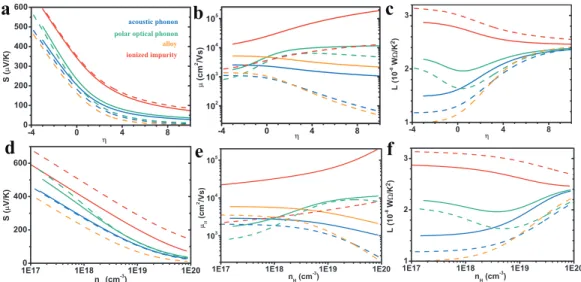
Other Carrier Scattering Mechanisms
- Ionized Impurity Scattering
- Neutral Impurity Scattering
- Deformation Potential Scattering from Optical Phonons
- Inter-valley/Inter-band Scattering
- Polar Scattering from Optical Phonons
- Alloy Scattering
The interband deformation potential of acoustic phonon scattering D is the same regardless of the start/end valley, it has the same unit as Ξ. The first part shows the same dependence on energy and temperature as equation 3.47 for the intraband strain scattering potential from acoustic phonons. 69 samples, the total relaxation time will still be well described using equation 3.47 with an effective strain potential Ξeff = 9 eV.
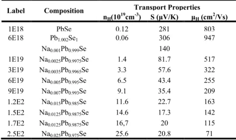
P-type PbSe with Na doping
- Introduction
- Sample Synthesis and Transport Properties
- Transport Property Modeling
- Thermoelectric Merit of Two-band Systems
In figure 4.3 this is also plotted for the undoped sample "1E18", the linear part of the plot was equipped with activation energy of 0.17 eV. Comparing data from Caltech as well as most published data on PbSe, as shown in Figure 4.6 a), the majority of results have suggested the same effective mass for the L conduction band and valence band. For B1 ≥ 0.3, the optimal η is always around the edge of the first band, regardless of the quality of the second band (Figure 4.15).
N-type PbSe Doped on Cation Site
Introduction
Sample Synthesis and Transport Properties
Temperature-dependent transport properties of In-doped PbSe a) resistivity, b) Seebeck coefficient, c) Hall mobility and d) thermal conductivity. This result shows that In-doped PbSe is almost as good as the Br-doped one. Transport properties as a function of temperature for Bi-doped PbSe a) resistivity, b) Seebeck coefficient, c) thermal conductivity, d) Hall mobility, e) Hall carrier density and f) zT.
Short-range Potential Scattering from Impurities
The present study suggested the presence of potential short-range scattering by revealing a difference in its magnitude between the dopant at the cation site and the dopant at the anion site. Furthermore, at low doping levels below 1 x 1019 cm-3 the impurities are so diluted that the potential short-range scattering is negligibly weak. Solid curve calculated with distortion potential and polar scattering without considering the short-range potential.
N-type PbS doped with Cl
- Introduction
- Sample Synthesis and Transport Properties
- Transport Property Modeling with Multiply Scattering Mechanisms
- Polar Scattering from Optical Phonon
The Hall mobility (µH = RH/r) decreases monotonically and smoothly with temperature, a dashed line is drawn representing the T-2.5 dependence, which is typical for Pb chalcogenides with deformation potential phonon scattering the dominant scattering mechanism, but is actually just true. for non-degenerate samples (when there is no bipolar influence), the temperature dependence becomes weaker as the increase of degeneracy, i.e. the carrier density, and for highly degenerate samples a T-2 dependence is more likely to be the case. 2] Equation 6.8 The same methodology works for more general cases when other scattering mechanisms such as the alloy scattering must be taken into account. From the result shown in Table 6.3, the polar scattering is important around room temperature in light doped lead chalcogenides.
Solid Solutions between Lead Chalcogenides
Introduction
Within the atomic substitution framework, a general measure of zT enhancement due to atomic disorder in solid solutions is derived that can be applied to several thermoelectric solid solutions, allowing convenient prediction of whether better thermoelectric performance can be achieved in a given solid solution. This criterion generally tells whether an improvement in zT can be expected if the band parameters of solid solutions can be approximated by the bond line between their constituent compounds.
Sample Synthesis and Transport Properties
- N-type PbTe 1-x Se x
- N-type PbSe 1-x S x
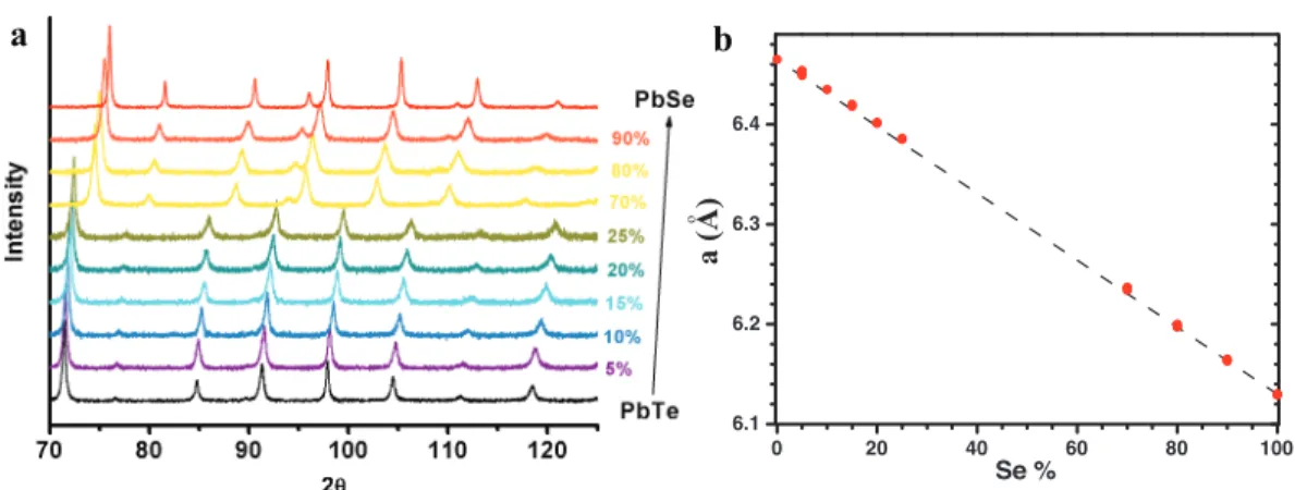
List of PbTe1-xSex solid solution samples and properties at 300 K. Figure 7.2. a) XRD lattice parameter for PbTe1-xSex and b) lattice constant calculated using the standard extrapolation method, typical solid solution behavior is seen. The carrier density of these samples is not reported, the chemical potential is thus estimated from the reported mobilities at both ends of PbTe and PbSe and was determined to be 1.7 (corresponding to nH ~ 1E19). Drift mobility at a) 300 K and b) 800 K for (PbTe)1–x(PbSe)x solid solutions with different doping levels. The experimental results and the calculated κL according to the point defect scattering thermal conductivity model at 300 K and 850 K are shown in Figure 7.15 regarding the reduction of the lattice thermal conductivity.
Alloy Scattering of Charge Carriers
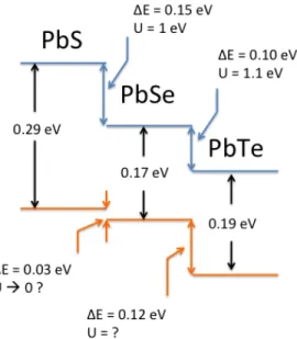
Although the scattering potential of the alloy U is not exactly the band offset ΔE, it is still reasonable to expect that U is proportional to ΔE. However, none of the measured mobilities from all three samples are significantly smaller than the calculated mobility for PbSe1-xSx without alloy scattering, suggesting a good probability that the alloy scattering is negligibly weak in p-type PbSe1-xSx. In general, the value of the alloy scattering potential U is critical for the magnitude of alloy scattering and mobility reduction in solid solutions.
Point Defect Scattering of Phonons
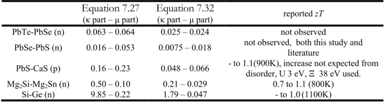
The assumption behind his derivation is, in addition to the high temperature approximation, that a combined scattering mechanism with Umklapp-type relaxation time for the unalloyed “pure” compound (this will allow the contribution of Normal process), and the only added scattering mechanism is the point defect which in the alloys or solid solutions scattered. In Table 7.5, the κL reduction is compared between different material systems with the same degree of alloying (30%), together with the magnitude of the contribution of mass (ΔM/M) and strain field (Δα/α and ε) contrast. The factor with the highest correlation with the thermal conductivity reduction (ΔκL/κL,pure) is the size of κL,pure.
Criteria of Beneficial Disorder for Thermoelectrics
The sign of Equation 7.26 determines whether the solid solution is advantageous (has a higher thermoelectric quality factor) compared to the pure compound. Thus, Equation 7.27 is greater than zero, a prerequisite for possible enhancement of zT by solid solution formation. In systems with theoretical insight into how doping affects the band structure, Equation 7.27 and Equation 7.32 can be used to predict the potential improvement in zT after adding these effects as additional terms on the left-hand side.
Introduction
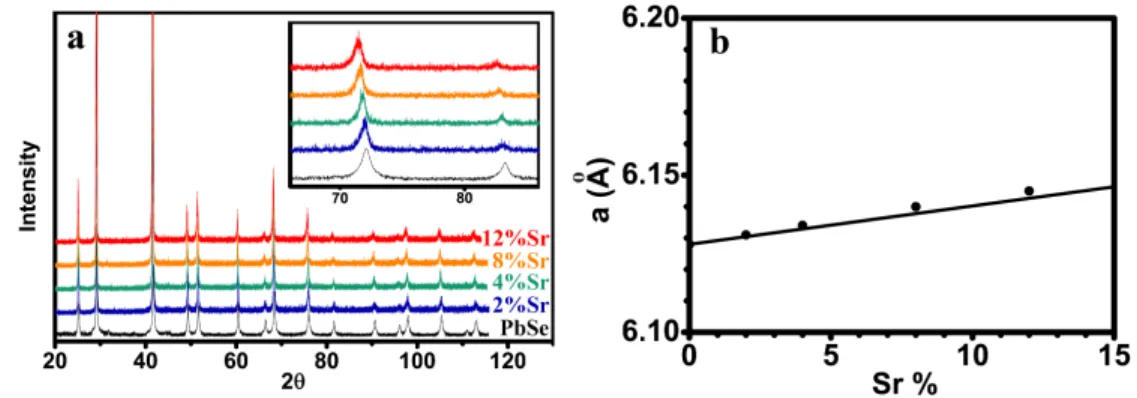
In both PbSe and PbTe, the maximum of the secondary valence band (along the Σ line of the Brillouin zone, called the Σ band) contributes to the carrier transport at high temperatures when the energy of the primary valence band (the L band) decreases as the band gap increases with temperature. Given the rock salt structure and the lattice parameter259 of 6.25 Å for SrSe, it is very likely that significant solubility of SrSe in bulk PbSe can be found. Our result shows that PbSe and SrSe form thermodynamically stable bulk solid solutions and that the solubility of SrSe in PbSe is as high as 8%.
Sample Synthesis and Microstructure
The effect of Sr on the band structure is revealed by both transport and optical absorption edge measurements. As a first step in the solid solution investigation, the phase composition and lattice parameter were studied by XRD on hot-pressed, undoped samples. solid solution behavior and Vegard's law are observed throughout the sample at 12% Sr, as shown in Figure 8.1. The inhomogeneity usually suggests a solubility limit, but here it is more likely to be due to insufficient mixing of Sr and slow diffusion across some grain boundaries.
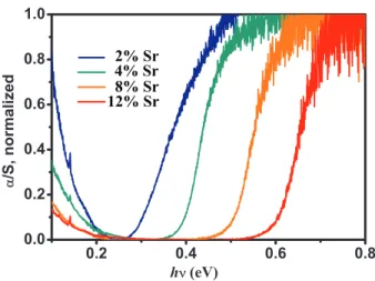
Changing of Valence Band Structure
Among Pb1-xSrxSe alloys, the Seebeck coefficient also increases with increasing Sr content. The calculated DOS for each composition (Figure 8.5 a)) shows a sudden rise around -0.1 eV, this is attributed to additional states in the Σ band and its position is used to estimate the gap between the L and Σ bands. Reduced energy gap between the two valence bands in Pb1-xSrxSe as a function of temperature, dashed line indicates 3kBT.
Transport Properties
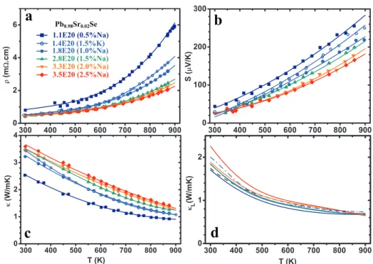
Figure 8.13 compares the temperature-dependent transport properties of Pb1-xSrxSe alloys with different Sr contents. This trend is observed in the entire temperature range up to 8% Sr. The higher values of S can be explained by the redistribution of carriers between the two valence bands, which populates more states in the band of high density of states Σ in alloys with more Sr, so that alloys with higher Sr content for a given carrier density have more carriers in the Σ band, so it is chemical potential closer to the band edge. Temperature dependence of a) resistance, b) Seebeck coefficient, c) Hall coefficient and d) thermal conductivity of Pb1-xSrxSe alloys.
Details on Modeling the Band Structure Change
The same U is taken for the conduction band, because so far no data are available for its more accurate evaluation, since due to the increased band gap and heavily doped samples, the conduction band parameter does not affect the final result very significantly. The smaller U for the heavy band is consistent with the assumption that the position of the heavy band does not explicitly depend on the Sr content. The relaxation time and mean free path are again related by l=. From now on, we will derive the expression for the Lorenz number.