Landau Damping Induced Limits in Nanogap Metal-Insulator-Metal Plasmonic Waveguides and Cavities
Thesis by
Daniel Rimoli Assumpcao
In Partial Fulfillment of the Requirements for the degree of
BACHELOR OF SCIENCE IN ELECTRICAL ENGINEERING
CALIFORNIA INSTITUTE OF TECHNOLOGY Pasadena, California
2019
© 2019
Daniel Rimoli Assumpcao ORCID: 0000-0002-0374-9901
ACKNOWLEDGEMENTS
I would like to thank my thesis advisor, Dr. Hyuck Choo, for serving as my research advisor over the past four years. Your support and guidance over the years has helped me develop technically and personally as a researcher.
I also would like to thank Dr. Shailabh Kumar and Dr. Radwan Siddique for being my postdoctoral mentors during my time in Choo lab. You guys have taught me countless skills and have given me the guidance needed to be a successful researcher.
Finally, I would like to thank the Caltech SURF Office, the Caltech-GIST collaboration fund, Samsung Advanced Institute of Technology, and the Kavli Nanoscience Institute for providing support and facilities to me over the years.
ABSTRACT
Plasmonic structures permit the focusing of light into volumes far below the diffraction limit. In particular Metal-Insulator-Metal (MIM) gap plasmonic structures can reach nanoscale energy confinement if the gap is sufficiently miniaturized. Under classical models, gap plasmonics can achieve indefinite confinement, down to the single atom level.
However, these classical models fail to consider quantum effects that occur as the
confinement approaches the single nanometer level. Recently, it has been demonstrated that Landau Damping, the absorption of highly confined plasmonic energy, is the dominant effect in highly confined MIM devices until the tunneling regime is reached. However, the effects of Landau Damping on MIM gap devices are poorly understood. In this work, we analyze the effects of Landau Damping on MIM gap devices, specifically MIM
waveguides and cavities. It is found that in waveguides, Landau Damping does not limit the confinement but does limit the maximum propagation length achievable. Moreover, in cavity structures, Landau Damping causes the Quality Factor to drop significantly as the gap is further miniaturized. In terms of quantum optics applications, this causes the
radiative spontaneous emission enhancement to actually decrease as the gap is miniaturized sufficiently and a saturation of the coupling-loss ratio limiting the achievement of strong coupling . These effects will limit the possibilities for high performance nanogap plasmonic devices.
TABLE OF CONTENTS
Acknowledgements………...iii
Abstract ………iv
Table of Contents………. v
List of Illustrations and/or Tables………vii
Nomenclature……….viii
Abbreviations ……….xii
Chapter I: Introduction to Plasmonics and Landau Damping ... 1
Applications of MIM Waveguides... 2
Applications of MIM Cavities for Quantum Plasmonics ... 3
Quantum Mechanical Effects in Extreme Confinement Plasmonics ... 5
Our Work ... 6
Chapter II: Calculating Landau Damping In MIM Waveguides ... 9
Introduction ... 9
Classical Local Simulations ... 10
Landau Damping Model ... 11
Landau Damping Simulation Methodology ... 13
Chapter III: Effects of Landau Damping in MIM Waveguides ... 17
Analytical Description of Damping in MIM Waveguides ... 17
Performance of MIM Waveguides with Decreasing Gap Sizes ... 20
Performance of MIM Waveguides with Different Wavelengths ... 23
Performance of MIM Waveguides with Varying Inner Dielectrics ... 24
Discussion ... 25
Chapter IV: Background on Metal-Insulator-Metal Cavities ... 31
Chapter V: Effects of Landau Damping in MIM Cavities ... 38
Performance of MIM Waveguides with Decreasing Gap Sizes ... 38
Effect of Wavelength on MIM Cavity Performance ... 43
Effect of Inner Dielectric on MIM Cavity Performance ... 45
Discussion ... 46
Chapter VI: Conclusion ... 56
References ... 58
Appendix A: Proposed Experimental Verification ... 63
Appendix B: Performance of MIM Waveguides in C-Band ... 70
Appendix C: Tunneling in MIM Waveguides ... 73
Appendix D: Simulation of MIM-Air Reflectivity ... 75
LIST OF ILLUSTRATIONS AND/OR TABLES
Number Page
2-1. Diagram of Methodology ... 21
3-1. Properties of the MIM waveguide versus gap thickness ... 33
3-2. Properties of the MIM waveguide versus incident wavelength ... 35
3-3. Properties of the MIM waveguide versus inner dielectric constant ... 36
4-1. Diagram of constant-gap MIM Cavity.. ... 43
5-1. Parameters of MIM Cavity versus Gap ... 56
5-2. Parameters of MIM Cavity versus Wavelength ... 58
5-3. Parameters of MIM Cavity versus Inner Dielectric Constant ... 60
A-1. Experimental Design ... 73
A-2. Experimental Simulations ... 75
B-1. Properties of the MIM waveguide versus gap in the C-band ... 77
C-1. Effects of tunneling on MIM waveguides ... 80
D-1. Reflectivity of air-MIM interface ... 82
NOMENCLATURE
Plasmonics: The study of the interaction of metals with light, and more specifically the coupling of light to the electrons in the metal. The field both explains the optical properties of metals helps to enable novel devices.
Surface Plasmon Polariton (SPP): An electromagnetic mode that exists at the interface between metals and dielectrics due to the coupling of incident photons and electrons in the metal. Unlike the electromagnetic modes of dielectric materials whose confinement is limited by the diffraction limit, SPPs can achieve energy confinement far below the free space wavelength of light. The confinement in an individual SPP mode is dependent on the materials and the incident free space wavelength.
SPP Gap Mode: A special type of SPP mode formed when two metals are separated by a dielectric gap. The individual SPPs on both interfaces interfere, forming a joint gap mode.
Due to the interference, the confinement of the energy is localized to the gap and thus is dependent on the size of the gap.
Metal-Insulator-Metal (MIM): Specific type of gap mode formed through having two metals separated by an inner dielectric layer. The inner dielectric layer is referred to as the gap. This arrangement allows the increase of confinement through miniaturizing the gap.
Under classical models, the confinement can be increased arbitrarily through further miniaturizing the gap. The primary goal of this work is to look at the practical limits to this confinement due to the onset of Landau Damping
Local / Classical Model: Refers to the use of classical electromagnetic expressions to describe plasmonic structures. Landau Damping is not taken into account in this model.
Landau Damping: Refers to in general the absorption of high wavevector waves in a plasma. In the context of plasmonic, refers to the absorption of highly confined electromagnetic energy in SPP modes due to the high wavevector enabling electronic transitions that were previously forbidden due to a momentum mismatch.
Intrinsic Damping: The damping in a material due to the material properties and in absence of Landau Damping.
Landau Damping Induced Damping: The damping induced by the onset of Landau Damping at high energy confinements. This summed with the intrinsic damping gives the total damping under the Landau Damping model.
Optical Waveguide: Structure that guides electromagnetic waves, restricting the expansion of the mode and thus the loss. They are integral to routing electromagnetic energy in highly compact settings, such as in integrated optical interconnects in integrated circuits.
Waveguide Mode: A solution to the electromagnetic differential equation describing a waveguide. It describes the distribution of the electromagnetic fields that will propagate in the waveguide. In this work, the mode always refers to the fundamental mode of the waveguide, meaning the one with no variation parallel to the metal-gap interface.
Wavenumber: The propagation constant of a waveguiding mode. The real part corresponds with the spatial frequency and the imaginary part with the losses.
Mode Length: A figure of merit for the confinement in a waveguide. It can be interpreted as the average length which the energy is spread over in a waveguide. It is calculated through dividing the total energy transferred in the waveguide by the energy at the center point.
Propagation Length: The length in the propagation direction over which the energy in the waveguide drops to 1/e of its initial value.
Optical Cavity: An electromagnetic resonator which stores optical energy through the interference of multiple reflection forming standing waves. Through placing matter in the cavity, the interaction between light and matter can be altered which has important applications in future quantum technology. The strength of the light and matter interaction in the cavity can be calculated through the cavity’s mode volume and quality factor.
Cavity Mode: A solution to the electromagnetic differential equations governing the behavior of the cavity. It represents a distribution of the electromagnetic field which oscillates in time but whose distribution remains constant.
Constant-Gap MIM Cavity: The MIM cavity structure considered in this work consisting of two rectangular cuboid metals sandwiching an inner dielectric layer. The gap between the metals is constant throughout the structure.
Mode Volume: Parameter of a cavity mode which describes the confinement of energy in the cavity. It represents the average volume which the energy of the cavity is spread over for a given mode.
Quality Factor: Parameter of a cavity mode which describes the energy loss in the system.
It is proportional to the number of oscillation cycles that the cavity can undergo before all energy in the system is lost.
Purcell Factor: Figure of merit indicating the strength of the light-matter interaction for an emitter placed in the cavity. It corresponds with the increase in the spontaneous emission rate of an emitter placed in the cavity due to the Purcell effect.
Purcell Effect: The enhancement of an emitter’s spontaneous emission rate through changing its optical environment. In the context of this work, the rate is changed through putting the emitter in an MIM optical cavity.
Single Photon Source: Device which deterministically emits a single photon on demand. It is a crucial building block for quantum telecommunication technology.
Radiative Spontaneous Emission Enhancement: The increase in the Spontaneous Emission of an emitter radiated from the cavity. It differs from the Purcell Factor because it refers to only the increase in photons radiated from the cavity, ignoring photons absorbed by the cavity. It is important for creating bright single-photon sources.
Strong Coupling: Regime in which the emitter and its cavity are significantly coupled such that their modes are perturbed, forming hybrid modes. Qualitatively, this occurs when a photon emitted by the emitter in the cavity is more likely to be reabsorbed by the emitter than emitted from the cavity. Strongly coupled cavity-emitter systems have important applications in quantum information processing as well as creating novel light-matter devices.
Coupling-Loss Ratio: Parameter quantifying the ratio between the coupling rate between a cavity and emitter, and the total loss in the system. Increasing this parameter sufficiently allows the system to enter the strong coupling regime.
ABBREVIATIONS
MIM – Metal Insulator Metal t – Gap thickness in MIM structure
𝐿𝑝𝑟𝑜𝑝- Propagation length of a waveguide mode M – Mode length of a waveguide mode
L – Length of the cavity
Q – Quality factor of a mode of a cavity V – Mode Volume of a mode of the cavity F – Purcell factor of a mode of the cavity
rSE – Radiative Spontaneous Emission Enhancement
C h a p t e r 1
INTRODUCTION TO PLASMONICS AND LANDAU DAMPING Using fabricated nanostructures to control light on the nanoscale has opened entirely new possibilities in a variety of fields including on-chip electro-optic integration and optical interconnects for computation [1-3], single molecule biosensing for integrated medical implant technology [4-7], and empowering future quantum information technology [8-10]. This combination of nanotechnology with photonics, called nanophotonics, utilizes the ability to confine light to the nanoscale to achieve these exotic phenomena. The achievable confinement with traditional dielectric nanophotonic technology, however, is limited to the micron or hundreds of nanometer scale due to the diffraction of electromagnetic waves. Nevertheless, this limitation can be overcome with plasmonic structures.
Plasmonics, a cornerstone of nanophotonics, combine metals with traditional dielectrics to bypass the diffraction limit [11]. Specifically, a novel surface electromagnetic mode called a Surface Plasmon Polariton (SPP) is created at the interface of the metal and dielectric due to the coupling of photons and collective oscillation of electrons in the metal [11]. This mode is localized to the interface, permitting confinement far below the dielectric diffraction limit at the expense of large losses due to the optical ohmic losses in metals.
Individual SPP modes have confinements dependent on a variety of design parameters such as the metal and dielectric used, and the freespace wavelength. However,
by combining two SPPs in proximity in a gap configuration, the two modes will interfere allowing much smaller confinements to be achieved [11]. In particular Metal-Insulator- Metal (MIM) structures, consisting of two metals separated by an inner dielectric layer, can achieve extremely high energy confinements with a large portion of the energy localized to the insulator layer [12, 13]. Moreover, the confinement is geometrically dependent on the insulator gap size, allowing the gap to be shrunk for further confinement.
Due to the confinement achievable with plasmonics, a variety of novel applications have been developed including devices for confined on-chip computation [14-16], single molecule sensing with Surface Enhanced Raman Scattering (SERS) [17- 19], planar optical metasurfaces [20-22], and single-photon sources [23-25] to name a few. In particular, integrated MIM waveguides and utilizing MIM cavities to increase light-matter coupling for quantum information applications have a large potential. They will now be discussed in detail to provide context for our work.
Applications of MIM Waveguides:
Electromagnetic waveguides guide the transmission of light from one point to another in a confined area. These devices have many uses, but one particularly impactful one is their integration into on-chip communications technology. Recently, dielectric waveguides have been integrated into electrical chips to provide intrachip and chip to chip communication at potentially faster rates while utilizing less energy than electrical interconnects [26]. However, when using dielectric materials, the size of the waveguide is limited by the diffraction limit. This limit, on the order of hundreds of nanometers, is far larger than the tens of nanometer size of modern-day transistors. There is a clear size
mismatch between the two that limits both the maximum density of optical interconnect technology and the ability to replace electrical interconnects. However, this limit can be overcome using plasmonic technology. The MIM mode can be used to construct waveguides unaffected by the diffraction limit. These MIM waveguides can be miniaturized far below the diffraction limit, and thus can be used to make compact on chip waveguides to potentially replace nanoscale electrical interconnects.
Beyond applications in on chip interconnects, the high confinement achievable with MIM waveguides permit new possibilities previously unreachable with dielectric material. For example, the confinement allows MIM waveguides to focus light and probe individual molecules. Already MIM waveguide structures have been integrated into scanning probes to permit single molecule spectroscopy [27, 28] and these devices can potentially be fabricated on chip to enhance single molecule detection for medical technology [14].
Applications of MIM Cavities for Quantum Plasmonics
Efficiently coupling of photons and atomic quantum emitter is a cornerstone for the realization of quantum information technology [24, 29]. Due to the comparatively small size of an atom as compared to the wavelength of light, the interaction between light and atomic emitters is normally weak. However, by integrating these emitters into electromagnetic cavities, which store electromagnetic energy within their confined volume, the light-matter interaction can be increased, and unique behavior can be attained. MIM cavities, formed by the truncation of an MIM waveguide, allow the confinement of energy far below that of dielectric cavities. Thus they can achieve large
cavity-emitter couplings [29]. Due to this, researchers have begun investigating these MIM cavities for quantum applications, forming the field of quantum plasmonics.
Two different regimes emerge depending on the strength of the cavity-emitter coupling. The first is the weak coupling regime. In this regime the spontaneous emission rate of the quantum emitter is increased through the Purcell Effect where the magnitude of the enhancement is dependent on the confinement of the cavity and its losses [29, 30].
This is particularly interesting for the creation of ultrabright single photon sources. Single photon sources, which deterministically emit a single photon a time, are a key building block of future quantum telecommunications technology [8]. However, the emission rate of quantum emitters, which act as single photon sources, is far too low to achieve practical communications technology. By coupling it to a cavity, this rate can be increased through the Purcell Effect. Plasmonic cavities are well suited for this, as theoretical work has shown they can achieve a two order of magnitude improvement over dielectric cavities due to their confinement [31]. Already there have been impressive experimental demonstrations of large rate enhancements, although larger enhancements are still desired [23, 25]. This is currently one of the primary objectives in quantum plasmonics [32].
If the cavity-emitter coupling is increased sufficiently, then the strong coupling regime is entered. In this regime, the coupling is sufficiently large such that the modes of the cavity and the emitter combine, permitting the control of matter using light for quantum information applications [33]. It has been difficult to achieve strong coupling with plasmonic nanocavities due to the large losses offsetting the high confinement [29].
Despite this, there has recently been demonstrations of single molecule strong coupling
at room temperature using an MIM cavity platform [34-37]. This platform can be further developed for both room-temperature quantum information applications as well as empowering novel light-matter interaction-based devices.
Quantum Mechanical Effects in Extreme Confinement Plasmonics
As seen above, there is a plethora of opportunities for MIM plasmonic devices all of which are enhanced by the extreme confinement achievable with the platform.
Moreover, the performance of these devices is linked to the achievable confinement.
However, the limits of confinement in these structures are poorly understood. Under the classical model, the energy of an MIM structure can be confined indefinitely through further miniaturization of the gap, allowing energy to be confined to atomic and subatomic volumes. However, this model fails to consider quantum mechanical effects that occur once the confinement approaches the nanometer level that may potentially limit performance [38]. These effects will be briefly reviewed here.
There are two effects that occur in highly confined nanogap MIM structures, plasmonic tunneling and Landau Damping. Tunneling occurs when the gap is sufficiently small so that charge can tunnel from one metal to another, creating another loss pathway that effectively eliminates the gap mode [39]. A combination of theoretical modeling and experimental work has demonstrated that tunneling begins to occur at optical frequencies in gaps of around 0.5nm [39-42]. Thus, it only occurs at extreme, potentially subatomic levels of confinement. Since a monolayer of many of the interatomic spacers that could be used for the fabrication of MIM structures is larger than this, tunneling is not necessarily technologically limiting.
At intermediate gap sizes between 0.5nm to around 10nm, Landau Damping occurs. In plasmonic dimers, researchers observed a shift and broadening of the resonances as compared to the classical models when gaps were in the above range.
These were phenomenologically modeled as nonlocal effects. A variety of nonlocal phenomenologically models with increasing levels of sophistication have been proposed and matched to experimental results [43-45]. More recently, it was proposed that all these nonlocal effects can be attributed to Landau Damping [46]. In a plasmonic context, Landau Damping refers to the absorption of high wavevectors of plasmonic energy.
When the spatial confinement of energy in a plasmonic structure is sufficiently high, the momentum of the SPP is large enough to drive previously momentum forbidden electronic transitions. This opens a new absorption pathway. Previous theoretical work demonstrated that the anomalous shift in nanosphere dimer systems could be explained by Landau Damping [47]. These effects occur at comparatively much larger gap sizes than tunneling, thus making it more significant to practical MIM technology. However, the effects of Landau Damping and the limits on performance it induces are poorly understood in many MIM systems.
Our Work
From the above discussion, MIM devices have very useful applications due to their confinement. Despite this, the limits on the performance of many fundamental MIM gap devices due to the introduction of quantum effects is poorly understood.
In this work, analytical and numerical techniques are used to study the effects of Landau Damping in MIM waveguides and constant-gap MIM cavities with single-
nanometer gaps. Moreover, we study how the magnitude of these effects can be changed through tuning of the wavelength and the dielectric constant of the inner dielectric.
Finally, Landau Damping’s impact on the suitability of waveguides and cavities for different applications is considered.
We determine that Landau Damping can be extremely harmful to the performance of nanogap plasmonic devices, limiting potential applications. Specifically, it is discovered that in MIM waveguides, Landau Damping does not limit the confinement but it both decreases and limits the maximum propagation length due to the introduction of the addition loss mechanism. In MIM cavities, this manifests as a significant drop in the quality factor as the gap is decreased. This causes the radiated Spontaneous Emission enhancement to decrease as the gap is miniaturized and the coupling-loss ratio for strong coupling to stagnate. In both platforms, it was found that using larger wavelengths and lower dielectric constants for the inner dielectric spacer minimized the effects of Landau Damping. This will be vital for the design and applications of future integrated plasmonic waveguides and nanocavities.
The thesis is organized as follows:
Chapter 2: The background of Landau Damping and studying the performance of MIM waveguides is discussed.
Chapter 3: An analysis of the effects of Landau Damping on MIM waveguides is presented
Chapter 4; The background for using Landau Damping to analyze MIM cavities is discussed.
Chapter 5: The effects of Landau Damping on MIM cavities is discussed Chapter 6: Conclusion
C h a p t e r 2
CALCULATING LANDAU DAMPING IN MIM WAVEGUIDES
Introduction
In this work analytical and numerical FEM simulations are used to determine the effects of Landau Damping in MIM plasmonic devices. Both are utilized since the analytical analysis provides an understanding of the reasoning behind the observed effects, but simulations allow for more robust results. This section discusses the background and methodology for integrating Landau Damping into traditional electromagnetic models for both the analytical and numerical calculations of the properties of MIM waveguides.
The device structure considered is shown in Fig 2a. It consists of an MIM waveguide with two metals sandwiching an inner dielectric layer of thickness t, and infinite in both the propagation direction and parallel direction. Beyond allowing us to study MIM waveguides, the behavior of MIM cavities is also calculated from the parameters of this model MIM waveguides as opposed to a direct calculation (see Chapter 4).
The relative permittivity of the metal was described by the Drude model [11]:
𝜀(𝜔) = 1 − 𝜔𝑝2
𝜔2+ 𝑖𝛾𝑖𝑛𝑡𝑟𝜔 (2 − 1)
where 𝜔 is the incident frequency, and 𝜔𝑝 and 𝛾 are material properties referring to the plasma frequency and damping of the metal respectively.
Two metals were considered, Ag, whose parameters were taken from the literature [48], and an ideal metal where the intrinsic damping was set to 0. The gap, incident freespace wavelength, and permittivity of the inner dielectric were all varied.
Only the fundamental mode of the waveguide is considered in this work.
There are three main parameters for a waveguide to understand its performance.
First there is the wavenumber, k of the waveguide which is the propagation constant of the mode and gives a sense of the confinement in the propagation direction. Second there is the propagation length 𝐿𝑝𝑟𝑜𝑝, which is defined as the length over which the plasmonic mode losses 1/e of its energy and corresponds with the loss of the waveguide. Finally, there is the mode length, M, of the mode which is the average length in the transverse direction which the energy is distributed over. It provides the best estimation of the transverse confinement of the waveguide. The exact expressions for these parameters are discussed below.
Classical Local Simulations
To solve for the waveguiding modes, a quasi 1D cross section of the waveguide was taken and the mode was solved for either using analytical or FEM simulations (COMSOL) [49]. Since a quasi 1D cross section was used, only the fundamental mode of the waveguide was solved for and all the calculations are based on the fundamental model. Fig 2b shows an example of a calculated electric field cross-section for an MIM waveguide
The simulation software solves the complex wavenumber 𝑘𝑚𝑜𝑑𝑒 of the waveguiding mode in addition to the E-field distribution. Then the different parameters of the mode can be calculated. The propagation length is given by [11]:
𝐿𝑝𝑟𝑜𝑝 = (2𝐼𝑚[𝑘𝑚𝑜𝑑𝑒])−1 (2 − 2) The mode length is calculated from the distribution of fields of the mode along the 1D cross-section using the following equation [11].
𝑀 =∫ 𝑢𝑒(𝑥)𝑑𝑧
𝑢𝑒(𝑥0) (2 − 3)
where 𝑢𝑒(𝑥) is the energy density of the electric field at a position x and x0 is the center of the waveguide. The energy density of the electric field at a position x for a Drude model metal is given by [50]:
𝑢𝑒(𝑥) =𝜀0
2 (𝑛2+2𝜔𝑛𝜅
𝛾 ) |𝑬(𝑥)|2 (2 − 4)
where 𝑬(𝑥) is the electric field at a position x, and 𝑛, 𝜅 are the real and imaginary parts respectively of the index of refraction of the material at a position x. Note that although the above equation applies for Drude-model metals, it also applies to lossless dielectrics where 𝜅 = 0. Thus, in the context of the simulations in this work, it can be applied to the entire MIM structure.
Note that in this work, “local” and “classical” both refer to this model.
Landau Damping Model
To account for Landau Damping, the local model needs to be extended. This can be done by adapting the dielectric constant of the metal from the Drude model to consider
the increased absorption pathways induced by Landau damping. Note that the following derivation in this section was adapted from ref [46] and is not unique to this work.
A more complete expression for the dielectric constant of a metal is given by the Lindhard model:
𝜀(𝜔, 𝑘) = 𝜀𝑏+ 3𝜔𝑝2
𝑘2𝑣𝐹2(1 − 𝜔
2𝑘𝑣𝐹𝑙𝑛𝜔 + 𝑘𝑣𝐹
𝑤 − 𝑘𝑣𝐹) (2 − 5) Let 𝑞 = 𝑘
𝑘𝐿𝐷 where 𝑘𝐿𝐷 = 𝑣𝐹/𝑤 and corresponds with the offset vector for Landau Damping. Now notice that as q > 1, the imaginary part of the dielectric constant begins to increase leading to losses in the material and is given by:
𝜀𝑖(𝜔, 𝑞) = 3 2𝜋 𝜔𝑝2
𝜔2𝑞3 (2 − 6)
This increase in the losses of the material is due to Landau damping. Thus, we have an expression for the imaginary part of the dielectric constant due to Landau damping at a given wavevector. Given a distribution of the electric field, E(r), the longitudinal Fourier transform can be taken to determine the power density for a given wavevector using the following equation:
|𝐹||(𝑘)|2 =|𝑭(𝑘) ∙ 𝑘|2
𝑘2 (2 − 7)
Where 𝑭(𝑘)is the Fourier transform of E(r). Then, by computing the overlap of this power density with the expression for the induced losses at a given k, the total imaginary part 𝜀𝑖 induced by Landau Damping of can be expressed as:
𝜀𝑖 = 3𝜋𝜔𝑝2
2𝜔2 ∫ 𝑞−3|𝐹||(𝑞)|2𝑑𝑞
∫ |𝑭(𝑞)|0∞ 2𝑑𝑞
∞ 1
(2 − 8)
This loss can be incorporated into the Drude model through adding an additional damping term 𝛾𝐿𝐷 so that the modified Drude model is given by:
𝜀(𝜔) = 1 − 𝜔𝑝2
𝜔2+ 𝑖(𝛾𝑖𝑛𝑡𝑟 + 𝛾𝐿𝐷)𝜔 (2 − 9)
Since in the Drude model, 𝜀𝑖 =𝜔𝑝2
𝜔3 𝛾𝐿𝐷, 𝛾𝐿𝐷 can be related to the E(r) and computed through the following formula:
𝛾𝐿𝐷 = 3𝜋𝜔
2 ∫ 𝑞−3|𝐹||(𝑞)|2𝑑𝑞
∫ |𝑭(𝑞)|0∞ 2𝑑𝑞
∞ 1
(2 − 10)
The above analysis demonstrates two points. First, the effects of Landau Damping can be fully accounted for using classical electromagnetic calculations based on the Drude model through adding an additional damping term to the models. Second, the additional damping term can be calculated from the electric field distribution of a mode using the formulas given above. This provides both the initial expressions from which the analytical expressions can be derived and a numerical method that can be implemented using FEM simulations.
Landau Damping Simulation Methodology
To implement the above formulas into FEM software, an iterative approach was used in ref [47] (Fig 2c). Initially the modes of the waveguide were calculated using just the intrinsic damping and not considering the Landau Damping induced damping rate.
After this, the field profile of this mode was taken and from it the Landau Damping
induced damping rate, 𝛾𝐿𝐷, was calculated using (2-10). This Landau Damping induced damping rate was then combined with the intrinsic damping to calculate the new permittivity of the metals, and the simulation was repeated. This whole cycle was repeated until the value for 𝛾𝐿𝐷 converged.
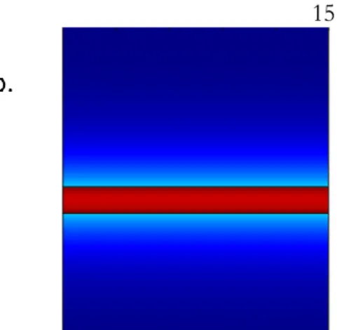
Figure 1: Diagram of Methodology. a. Diagram of the model Metal-Insulator-Metal waveguide considered in this work consisting of two metals sandwiching an inner dielectric layer with variable gap thickness. Note that the waveguide is infinite in all directions but the transverse (gap) direction. b. A plot of the electric field intensity distribution for an example fundamental mode of the MIM waveguide, showing most of the electric field is concentrated in the dielectric gap with no variations parallel to the metal-air interface. c. The methodology for simulating the behavior of the waveguide when considering the Landau Damping induced losses. An iterative approach is used, where the waveguide mode is first solved under the local model, the induced Landau
damping rate due to the E-field distribution is calculated, and then this additional damping term is incorporated back into the metal’s optical parameters and the simulation is repeated. This is repeated until the damping term converges.
C h a p t e r 3
EFFECTS OF LANDAU DAMPING IN MIM WAVEGUIDES The MIM waveguide is the most fundamental gap plasmonic device. It has important applications and can be used to describe more sophisticated MIM plasmonic devices [15, 51]. The high confinement is key to the performance of these waveguides, and thus it is important to understand both how Landau Damping introduced at these high confinements limits the performance and how the waveguides can be engineered to overcome these limitations.
Analytic Description of Damping in MIM Waveguides
First we derive an analytical expression for the damping rate induced by Landau Damping in MIM waveguides at high confinements Since Landau damping does not change the wavenumber of the waveguiding mode (see simulations below), the relation between the wavenumber of the mode and the induced damping rate can be combined with the dispersion relation of MIM waveguides to provide an accurate analytical solution. This allows a more concrete understanding of the trends of Landau damping in waveguides than could be provided by simulation results alone.
It will be assumed that 𝑘𝑚𝑜𝑑𝑒 ≪ 𝑘𝐿𝐷 where 𝑘𝐿𝐷 is the offset vector for Landau Damping as given by 𝑘𝐿𝐷 = 𝑣𝐹/𝑤. This assumption is valid because 𝑘𝐿𝐷 corresponds with spatial frequencies of ~0.5nm, which is well below most waveguides considered in this work.
The magnitude of the electric field perpendicular to the propagation direction within the metal can be written as [11]:
𝐸𝑝𝑒𝑟𝑝 = 𝐶𝑘𝑚𝑜𝑑𝑒𝑒−𝑘𝑝𝑒𝑟𝑝𝑥 (3 − 1) Where C is a proportionality constant, 𝑘𝑝𝑒𝑟𝑝 is the decay rate of the field in the metal, and x is the position in the metal where 0 is defined at the metal-dielectric interface.
Similarly, the electric field in the direction of propagation is given by [11]:
𝐸𝑝𝑎𝑟𝑎𝑙𝑙𝑒𝑙 = −𝑖𝐶𝑘𝑝𝑒𝑟𝑝𝑒−𝑘𝑝𝑒𝑟𝑝𝑥 (3 − 2) The perpendicular wave vector can be related to the wavenumber of the mode through the wave equation [11]:
𝑘𝑝𝑒𝑟𝑝2 = 𝑘𝑚𝑜𝑑𝑒2 − (2𝜋 𝜆 )
2
𝜀𝑚 (3 − 3)
If we assume high confinement, then 𝑘𝑚𝑜𝑑𝑒 ≫ (2𝜋
𝜆)2𝜀𝑚 so 𝑘𝑝𝑒𝑟𝑝≈ 𝑘𝑚𝑜𝑑𝑒 and thus |𝐸𝑝𝑒𝑟𝑝| = |𝐸𝑝𝑎𝑟𝑎𝑙𝑙𝑒𝑙|, simplifying the calculation
Next the spatial power density for either the parallel or perpendicular direction is calculated by taking the Fourier transform of the electric field distribution:
𝐹(𝑘) = 𝐶𝑘𝑚𝑜𝑑𝑒
𝑘𝑚𝑜𝑑𝑒+ 𝑖𝑘 = 𝐶 1 + 𝑖 𝑘
𝑘𝑚𝑜𝑑𝑒
(3 − 4)
Where k is the spatial wavevector perpendicular to the metal-dielectric interface.
The longitudinal Fourier transform is given by (2-7):
|𝐹||(𝑘)|2 =|𝑭(𝑘) ∙ 𝒌|2
𝑘2 =|𝐹𝑝𝑒𝑟𝑝(𝑘) ∙ 𝑘|2+ |𝐹𝑝𝑎𝑟𝑎𝑙𝑙𝑒𝑙(𝑘) ∙ 𝑘𝑚𝑜𝑑𝑒|2
𝑘2 (3 − 5)
However, note our earlier assumption that 𝑘𝑚𝑜𝑑𝑒 ≪ 𝑘𝐿𝐷. This ensures that when the integral of the longitudinal transform is taken, 𝑘𝑚𝑜𝑑𝑒 ≪ 𝑘 and thus the parallel field contribution to the Landau Damping can be neglected to obtain:
|𝐹||(𝑘)|2 = |𝐹𝑝𝑒𝑟𝑝(𝑘)|2 (3 − 6) The final step is to evaluate the two integrals in the equation for the Landau Damping induced damping (2-10). We assumed that 𝑘𝑚𝑜𝑑𝑒′ ≫ 𝑘𝑚𝑜𝑑𝑒′′ to simplify the calculation.
These integrals will be evaluated individually:
1
𝑘𝐿𝐷∫ |𝑭(𝑘)|2𝑑𝑘
∞ 0
= 1
𝑘𝐿𝐷∫ (|𝐹𝑝𝑎𝑟𝑎𝑙𝑙𝑒𝑙(𝑘)|2+ |𝐹𝑝𝑒𝑟𝑝(𝑘)|2) 𝑑𝑘 =
∞ 0
𝐶2
𝑘𝐿𝐷∙ 𝜋𝑘𝑚𝑜𝑑𝑒′ 1
𝑘𝐿𝐷∫ ( 𝑘 𝑘𝐿𝐷)
−3
|𝐹||(𝑘)|2𝑑𝑘
∞ 𝑘𝐿𝐷
= 𝑘𝐿𝐷2 ∫ 𝑘−3 𝐶2 1 + ( 𝑘
𝑘𝑚𝑜𝑑𝑒′ )
2𝑑𝑘
∞ 𝑘𝐿𝐷
≈ 𝑘𝐿𝐷2 𝐶2∫ 𝑘−3 1 ( 𝑘
𝑘𝑚𝑜𝑑𝑒′ )
2𝑑𝑘
∞ 𝑘𝐿𝐷
= 𝑘𝐿𝐷2 𝐶2𝑘𝑚𝑜𝑑𝑒2 ∫ 𝑘−5𝑑𝑘
∞ 𝑘𝐿𝐷
= 𝐶2(𝑘𝑚𝑜𝑑𝑒′ )2
4𝑘𝐿𝐷2 (3 − 7)
The simplification in the second integral is due to the earlier assumption that 𝑘𝑚𝑜𝑑𝑒 ≪ 𝑘𝐿𝐷. Finally, evaluating the induced damping:
𝛾𝐿𝐷 = 3𝜋𝜔
2 ∫ 𝑞−3|𝐹||(𝑞)|2𝑑𝑞
∫ |𝑭(𝑞)|0∞ 2𝑑𝑞
∞ 1
=3
8𝑣𝑓𝑘𝑚𝑜𝑑𝑒′ (3 − 8)
Thus at large confinements, the induced damping in MIM waveguides is proportional to the real part of the wavenumber of the mode. The wavevector for an MIM mode is given by [52]:
𝑘𝑚𝑜𝑑𝑒= 2𝜋
𝜆 √𝜀𝑔+ 2𝜁[1 + √1 +𝜀𝑔− 𝜀𝑚
𝜁 (3 − 9)
Where 𝜀𝑔 is the dielectric permittivity of the gap, 𝜀𝑚 is the permittivity of the metal, and
𝜁 = (2𝜋𝜀𝑚 𝜆𝜀𝑔 𝑡)
−2
(3 − 10)
Thus, by iteratively solving both equations, 𝛾𝐿𝐷 can be numerically estimated.
However, since additional damping does not significantly change the real wavenumber of an MIM mode, 𝑘𝑚𝑜𝑑𝑒 can be computed using the intrinsic damping constants and then used to calculate 𝛾𝐿𝐷 without significantly sacrificing accuracy, permitting the above to give an accurate analytical solution.
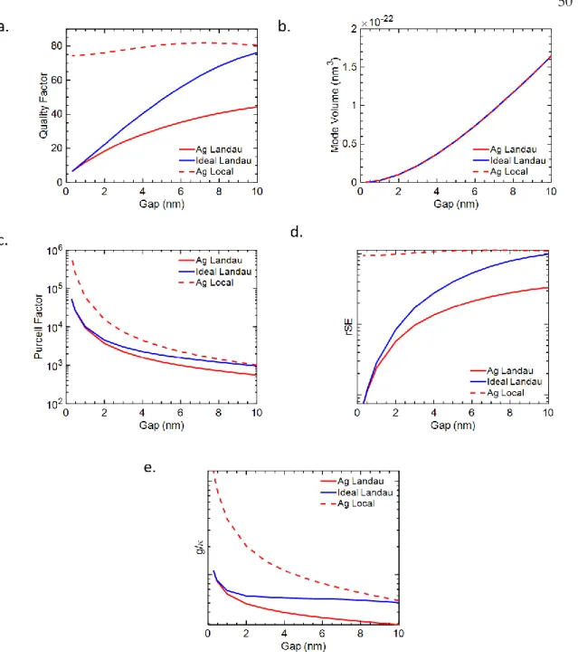
Performance of MIM Waveguides with Decreasing Gap Sizes
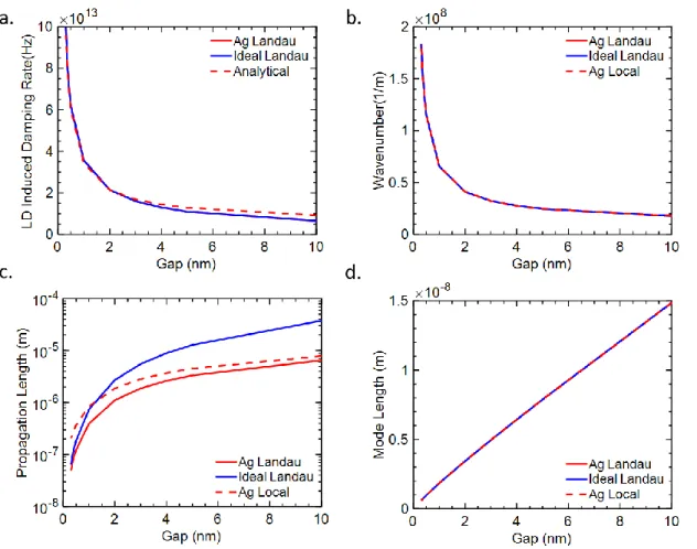
Having now an expression for the induced damping, FEM simulations under the classical and LD models (see section 2), were performed to numerically verify the analytical expression and understand its ramifications. The fundamental mode of an infinite Ag-air-Ag waveguide at an incident free space wavelength of 850nm was considered while the thickness of the gap, t, was varied.
Both the simulated induced damping rate due to Landau damping as well as the value calculated using the analytical equations are displayed in Fig 1a. The analytical expression shows excellent agreement with the FEM simulations, particularly at small gaps where the high confinement assumption is most valid.
We observe that the surface damping increases as the gap is miniaturized, due to the increased energy confinement. At a gap of 1nm, the LD induced damping rate has exceeded the intrinsic damping of Ag of ~3·1013 , becoming the dominant loss mechanism.
Empirically, the Landau damping rate is roughly proportional to the inverse of the gap length. As an MIM waveguide is further miniaturized, the analytical expression for its wavenumber given by 3-9 approaches a simpler form [51]:
𝑘𝑚𝑜𝑑𝑒≈ −2𝜀𝑔
𝜀𝑚𝑡 (3 − 11)
Since the induced damping is proportional to the real part of the wavenumber, we observe that
𝛾𝐿𝐷 ≈ 𝑅𝑒 (−3 4
𝑣𝑓𝜀𝑔
𝜀𝑚𝑡) ≈ −3 4
𝑣𝑓𝜀𝑔 𝜀𝑚′ 𝑡 ∝1
𝑡 (3 − 12)
Thus explaining the empirically observed ∝1
𝑡 dependence of the damping rate at small gap sizes.
Having verified the accuracy of the analytical expression and FEM simulations, the simulations were used to understand the effects Landau Damping caused through computing the different properties of the waveguide mode. The dispersion relationship of the mode shows no change due to the inclusion of Landau Damping as opposed to the local model (Fig 1b). Mathematically, this is since the additional damping term primarily causes a change in the imaginary part of the dielectric constant. Thus, the real part of the mode, the wavevector, is left unchanged. Therefore the analytical expression for the Landau Damping model need not be solved iteratively to obtain to high accuracy.
The propagation length in the Landau Damping model, on the other hand, is considerably smaller than under the classical models particularly at small gaps (Fig 1c). At 1nm, the propagation length is half of what is predicted by the classical model. To understand the ramifications of this, an MIM waveguide with an ideal metal with no intrinsic loss was
considered. Under classical models this lossless waveguide would have an infinite propagation length, providing a solution for plasmonics’ biggest issue. Under the Landau Damping model, however, loss is introduced due to Landau Damping and the propagation length is below a micron at a gap size of 1nm. The fact that an ideal, lossless model still has such a low propagation length due to Landau Damping indicates that Landau Damping caps the maximum achievable propagation length. Moreover, at small gap sizes, the maximum achievable performance is not significantly better than can what be currently achieved with Ag.
Finally, the effect Landau Damping has on energy confinement was considered through calculation of the mode length of the waveguide (Fig 1d). No change is seen between the mode length calculated for both the classical models and Landau Damping models. Thus, in these MIM waveguides, Landau Damping does not limit the maximum achievable confinement. This fact had previously been proposed in ref [47], where it was expressed that due to the boundary conditions of an MIM waveguide, the mode would be unable to spread out unlike what was seen in other systems. This also can be explained by the lack of change in the wavevector. At high confinements, (see Analytical sections), 𝑘𝑝𝑒𝑟𝑝≈ 𝑘𝑚𝑜𝑑𝑒 where 𝑘𝑝𝑒𝑟𝑝 is the rate of exponential decay of the electric field. A lack of change in the wavevector between the two models indicates no significant change in 𝑘𝑝𝑒𝑟𝑝, corresponding with a lack of change in the achieved confinement. Thus, Landau Damping does not limit the confinement and the only limit to the confinement achievable with MIM waveguides is due to the onset of tunneling at ~0.5nm (see Appendix).
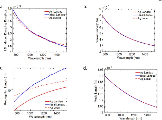
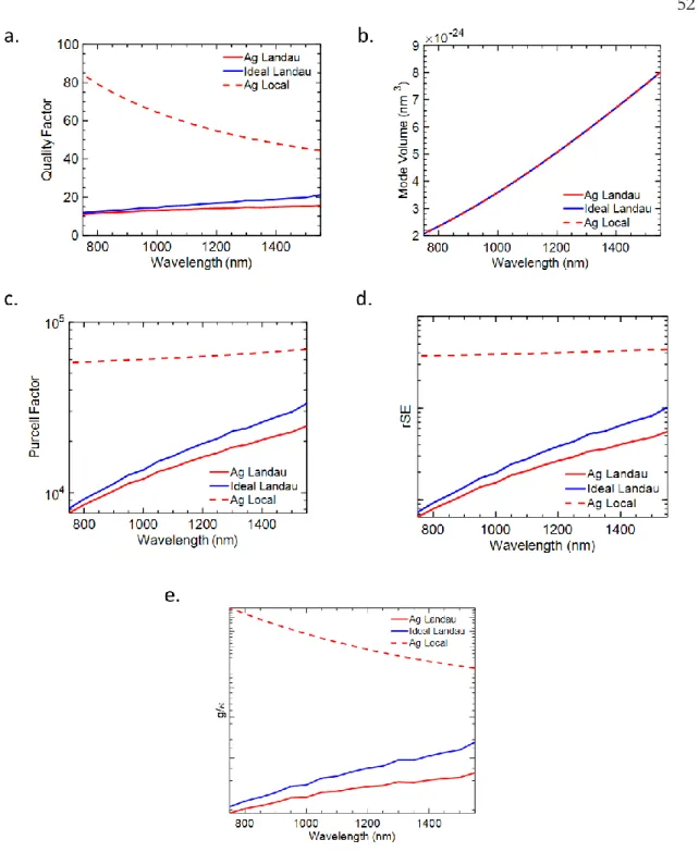
Performance of MIM Waveguides with Different Wavelengths
Beyond understanding how Landau Damping affects the performance of MIM waveguides, it is crucial to understand how the magnitude of these effects can be altered through playing with different parameters of the waveguide, specifically the incident wavelength and the inner dielectric used.
The magnitude of Landau Damping versus changes in the incident freespace wavelength was simulated where the gap was fixed to 1nm (Figure 2). We observe that the induced damping rate is increased as the wavelength is decreased and again showing good agreement between the FEM simulated damping rates and the analytical expressions (Figure 2a). In the expression for 𝛾𝐿𝐷, the only wavelength dependent term is 𝑘𝑚𝑜𝑑𝑒. It was also observed that the wavenumber does increase with smaller wavelength (Figure 2b). Thus, the increase in 𝑘𝑚𝑜𝑑𝑒 as the wavelength increases leads to additional confinement within the metal and that is fully responsible for the higher damping.
The propagation length versus wavelength was calculated (Figure 2c). The propagation length is significantly longer for larger wavelengths due to the much smaller induced damping rate. For example, at a gap of 1nm and wavelength of 1550nm, the propagation length was 2 microns for the ideal case, four times the propagation length at a wavelength of 850nm. This provides one avenue for minimizing the impact of Landau Damping, as at longer wavelengths even at a gap of 1nm, the propagation length is still comparatively large.
The wavenumber and mode length were calculated, and no significant change is seen through the introduction of Landau Damping as before (Figure 2b/d). The mode length
shows a slight increase at smaller wavelengths as has been observed in the literature, but the magnitude of the change is comparatively small.
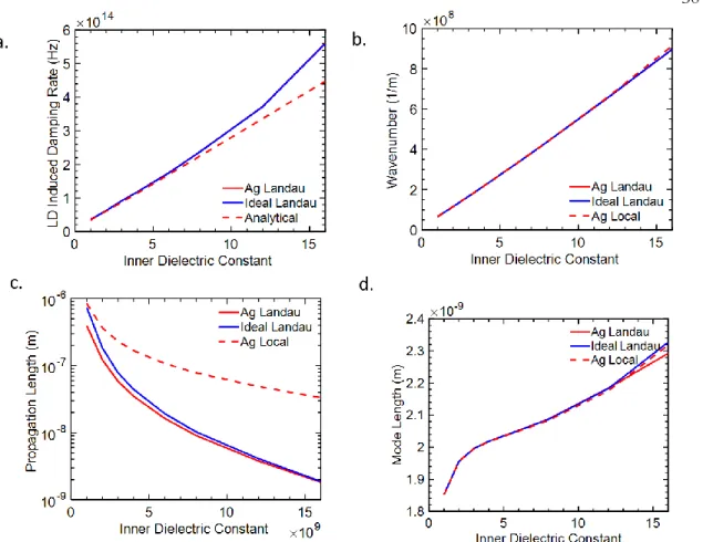
Performance of MIM waveguides with Varying Inner Dielectric Constant
The effect of the dielectric constant of the inner dielectric on the performance of MIM waveguides was examined. The value of the dielectric constant was varied with the gap fixed at 1nm and the wavelength fixed at 850nm (Figure 3).
The LD induced damping rate is shown in Figure 3a. An increase in the dielectric constant leads to a significantly larger damping rate. The increase in the dielectric constant leads to a larger wavevector of the mode which causes higher confinement of the electric field within the metal and thus a higher induced damping rate (Figure 2b). Looking at the analytical expressions, the wavevector of the waveguide mode at high confinements 𝑘𝑚𝑜𝑑𝑒 ∝ 𝜀𝑔 (3-11), and thus 𝛾𝐿𝐷 ∝ 𝜀𝑔, explaining the quasi-linear relationship with the inner dielectric constant observed in both the wavenumber and induced damping rate. Note that at high values of the dielectric constant, the analytical induced damping term and the simulated damping diverge due to the extremely high wavenumber of the mode challenging the 𝑘𝑚𝑜𝑑𝑒≪ 𝑘𝐿𝐷 assumption made in the analytic derivation.
The magnitude of this change in the damping rate is quite large as the inner dielectric increases due to this linear relationship. For example, at a gap of 1nm, the induced damping rate is an order of magnitude higher for an inner dielectric constant of 12 then it is for an 1nm gap with an inner dielectric constant of 1. These dielectric constants roughly corresponds to the constants of a high-index semiconductor such as GaAs and air, respectively.
We examined the effect of this increased Landau Damping on the propagation length (Figure 3b). The increased Landau Damping at larger dielectric constants leads to a significant drop in the propagation length. At a gap of 1nm and an inner dielectric constant of 16, the propagation length is around 2nm, a tiny amount over an order of magnitude lower than what the classical model predicts and two orders of magnitude lower than what is achieved at a dielectric constant of 1. This demonstrates how detrimental Landau Damping can be to the operation of waveguides, particularly high index waveguides.
Discussion
From the above results, Landau Damping’s biggest effect is that it severely limits the maximum achievable propagation length. Moreover, for small gap sizes this maximum propagation length is not much better than what can be achieved using low loss bulk metals such as Ag, indicating no potential significant improvement from a materials perspective
This point is particularly impactful for using MIM waveguides in integrated photonic applications to compactly send information at high densities. For intrachip and inter-chip communication, the information must be sent over a non-negligible distance larger than the 1 micron achievable at a gap of 1nm. This provides a practical cap on the minimum usable gap size that is dependent on the minimum propagation length required.
However, the results also demonstrate that through choose the design wavelength as well as inner dielectric intelligently, the effects of Landau Damping can be minimized, maximizing the optimal propagation length. For example, the simulations assumed a wavelength in the 850nm fiber optic band, but if larger wavelengths are used such as the C-
band (1550nm) the optimal propagation length can be increased by almost an order of magnitude (see Appendix for additional simulations at 1550nm). Moreover, the inner dielectric should be kept as low as possible to minimize the induced damping rate. Through engineering of these properties, plasmonic MIM waveguides can find a use for compact, short distance information transfer and then potentially integrated with dielectric waveguides for longer distance information transfer. Finally, 2D materials do not display this same out of plane Landau Damping and thus could be investigated as a possible avenue for overcoming this limit [53].
The onset of Landau Damping does not provide a limit on the achievable confinement, however. Thus, the gap can be miniaturized down to 0.5nm, at which the loss due to tunneling becomes dominantly lossy (see Appendix). This ensures bulk metal MIM waveguides can focus light down to the single atomic layer, the ultimate limits of confinement. Not only does this permit high-density integrated waveguides as discussed above, it also permits the focusing of light to probe individual molecules for sensing applications or fundamental study. Thus, the fundamental benefit of plasmonics, the extreme confinement achievable, is not limited by Landau Damping.
Figure 1. Properties of the MIM waveguide versus gap thickness. a. The induced Landau damping rate simulated for an Ag and an ideal metal waveguide as a function of gap thickness (curves are overlapped) as well as calculated using the analytic formula. The damping rate significantly increases as the gap is miniaturized and exceeds the intrinsic damping of Ag at 1nm. There is good agreement between the analytic and simulated values, particularly at small gap values. b. The wavenumber of the mode versus gap thickness for Ag under the classical local model and the Landau Damping model, showing no significant difference. c.
Propagation length versus gap size for Ag under the classical and Landau Damping models, as well as an ideal metal with no intrinsic damping under the Landau damping model. Landau Damping causes a significant decrease in the propagation length of the waveguide, and
severely limits the maximum achievable propagation length as seen from the ideal metal’s propagation length. (d) The mode length of the waveguide, showing no change between the Landau Damping and classical models. This indicates that Landau Damping does not limit the achievable confinement in the waveguide.
Figure 2: Properties of the MIM waveguide versus incident wavelength. a. The Landau Damping induced damping rate versus wavelength, showing an increased damping rate as the wavelength is shortened. b. Wavenumber versus wavelength, again showing no change between the classical and Landau Damping models and following the same trend at small wavelengths as seen in the induced damping rate. c. The propagation length versus wavelength, showing a considerable improvement at longer wavelengths due to lower induced Landau Damping rate. This provides one possible avenue to limit the effects of Landau Damping. d. The mode length versus wavelength, again showing no change between the classical and Landau Damping models and showing a comparatively small dependence on the wavelength.
Figure 3: Properties of the MIM waveguide versus inner dielectric constant. a. The Landau Damping induced damping rate versus inner dielectric constant, showing a large, quasi-linear increase as the dielectric constant increases. The analytical and simulation values diverge at large dielectric constant values due to the violation of the assumptions the analytical solution was based on. b. Wavevector versus inner dielectric constant, showing a linear increase which explains the large increase in the induced damping rate. c. The propagation length versus inner dielectric constant, showing a significant decrease and a sub- 10nm propagation length at high dielectric constants. d. The mode length of the simulated waveguides, showing only slight changes as the dielectric constant is varied.
C h a p t e r 4
BACKGROUND ON METAL-INSULATOR-METAL CAVITIES When a waveguide is truncated, the light is reflected at the truncated end, causing light to be trapped in the device and thus forming a cavity. This localizes the energy to the center of the structure, enhancing the interaction between light and matter and enabling many quantum optics applications [29]. Plasmonics, due to their high confinement, are particularly suitable for this application.
In this section, the background methodology for analyzing constant-gap MIM plasmonic cavities is discussed. The two key cavity parameters, the quality factor and mode volume will be calculated. Moreover, these cavities’ suitability for two potential quantum optics applications: single photon sources and achieving strong coupling between light and matter, will be analyzed. Due to the large number of variables and assumptions in this section, analytical expressions will not be rigorously derived and instead will just be used to explain trends through proportionality arguments. In addition, the focus will be on trends as opposed to absolute values to ensure the generality of the results. This chapter goes over the methodology and the actual results are in the next chapter.
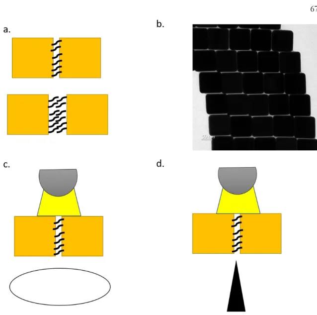
Rectangular cuboid constant-gap MIM cavities were considered (Fig 1). They consist of two finite length metals sandwiching an inner dielectric gap layer, which is just the waveguide considered previously but now truncated in the two infinite dimensions. The gap is constant across the cavity, allowing it to easily be described by the underlying waveguiding mode. The width was fixed to 350nm, a varying gap was used, and finally the length was set
such that the first order resonance in the length direction occurred at the chosen wavelength. This was done by setting the length to:
𝐿 = 𝜋
𝑅𝑒(𝑘(𝑡)) (4 − 1)
Where L is the length of the cavity, and k is the wavenumber of the MIM mode with gap size t . This is done so that the first resonance will still occur at the design wavelength regardless of the gap size or other parameters used. Thus, only the first resonance is ever considered in this work. In addition, it should be noted that the only modes of concern are those that are confined in the small gap layer which vary only along the length direction.
There are two primary parameters for cavities, the mode volume (V) and the quality factor (Q). V, similar to the mode length for waveguides, is the average volume which the energy is spread out over, quantifying the confinement. A smaller V indicates smaller confinement, and thus better coupling to emitters for quantum optics applications. Q quantifies the loss of the cavity, specifically referring to the ratio between the power stored in the resonator and the power lost per oscillation. A higher Q indicates the energy is stored in the cavity longer, allowing for better coupling to an embedded emitter and thus superior for quantum optics applications. A dimensionless figure of merit, the Purcell factor can be defined that is proportional to the Q/V of the cavity. The Purcell Factor refers to the proportion of spontaneous emission increase for an emitter placed within the cavity due to the Purcell Effect.
Q and V were calculated based on the mode parameters of their waveguiding cross section. This is done by considering the cavity as a traditional Fabry Perot cavity whose propagation characteristics are defined by the modes of the underlying waveguide. This allows us to apply the intuition built up in the previous chapter to this new domain.
The Q of the primary resonance of an MIM cavity can be related to its cross-sectional waveguiding parameters through the following equation [51]:
𝑄 = 2𝜋𝑛𝑔𝐿 𝜆 (1 − √𝑅𝑒−
𝐿 2𝐿𝑝)
(4 − 2)
Where 𝑛𝑔 is the group velocity and is given by 𝑛𝑔 = 2𝜋
𝜆∙𝑘(𝐺)− 𝜆 𝜕
𝜕𝜆( 2𝜋
𝜆∙𝑘(𝐺)), 𝜆 is the free space wavelength, 𝐿𝑝 is the propagation length, and R is the reflectivity at the air-MIM interface. The value of R was computed using FDTD simulations (see Appendix). The phase change of this reflection was assumed to be negligible. To evaluate the derivative for the group velocity, the analytical expression for the wavevector modes of the MIM cavity was used (see eq 3-9). For the dielectric of the metal, the Drude model was used as before with the damping of the metal set to its intrinsic value under the classical model and set to the sum of the intrinsic and the Landau Damping induced damping rate calculated in the previous section under the Landau Damping model.
The mode volume was estimated geometrically. It was assumed that the mode will exist only in the gap between the two metals and will be negligible on the other surfaces and in free space. This assumption is valid due to the high confinement in the plasmonic
structures as well as the loss being dominated by materials losses as opposed to radiative losses. Within the gap, the field was assumed to be approximately uniform in the width direction. This is valid since the comparatively large width of the structure will prevent significant variations in that direction. Along its length the field was assumed to vary as ∝ sin(𝜋
𝐿𝑧), due to the fact we are analyzing the primary mode of the cavity. In the transverse height direction, the energy is assumed to be spread out over the mode length previously calculated for the MIM waveguide. These assumptions result in the following expression for the mode volume that can be computed just using the geometry and the mode length:
𝑉 =∫ 𝑢𝑉 𝑒(𝑟)𝑑𝑟
𝑢𝑒(𝑟𝑐) =∫ ∫ ∫ 𝑢1𝐷,𝑒(𝑦) sin2(𝜋
𝐿𝑧) 𝑑𝑧𝑑𝑥𝑑𝑦
𝑊 0 𝐿 0
𝑢1𝐷,𝑒(𝑦0)
= ∫ sin2(𝜋
𝐿𝑧) 𝑑𝑧 ∫ 𝑑𝑥 ∫ 𝑢1𝐷,𝑒(𝑦) 𝑢1𝐷,𝑒(𝑦0)
𝑊
0 𝐿
0
𝑑𝑦 = 𝐿
2· 𝑊 · 𝑀(𝐺) (4 − 3)
Where L and W are the length and the width of the cavity, and M is the mode length for the waveguide mode for the given gap thickness as calculated in the previous section.
From Q and V, the Purcell factor for the MIM cavities was computed using the following formula to provide a figure of merit for the cavity[29]:
𝐹 = 3 4𝜋2( 𝜆
√𝜀𝑔
)
3𝑄
𝑉 (4 − 4)
Finally, two possible uses for these MIM cavity were evaluated: enhancing the radiative spontaneous emission rates and achieving strong coupling between light and matter.
The former is important for the realization of high rate single photon sources, one of the
biggest opportunities for quantum plasmonics [24]. The second is vital for a variety of quantum optics applications.
To understand the rate enhancement, the radiative spontaneous emission rate was considered. This differs from the Purcell Factor given above because the Purcell factor gives the total spontaneous emission (SE) rate and does not consider the proportion of the photons radiated out of the cavity versus absorbed by the metal. This radiated SE rate enhancement
is given by the following equation
[31]
𝛾𝑆𝐸
𝛾0 = 𝐹 𝛾𝑟𝑎𝑑
𝛾𝑡𝑜𝑡𝑎𝑙 (4 − 5)
where 𝛾𝑆𝐸
𝛾0 is the radiated SE enhancement, 𝛾𝑟𝑎𝑑 is the radiation rate, and 𝛾𝑡𝑜𝑡𝑎𝑙 is the total decay rate. The radiative rate can be written as [31]
𝛾𝑟𝑎𝑑 ∝ 𝜔𝑉
𝜆 (4 − 6)
Thus, the resulting expression for the emission enhancement is:
𝛾𝑆𝐸 𝛾0 ∝ 𝐹𝑉
𝜆 𝜔
𝛾𝑡𝑜𝑡𝑎𝑙 = 𝐹𝑉
𝜆𝑄 ∝ 𝑄2 (4 − 7)
The other possible application for plasmonic MIM nanocavities is to enter the strong coupling regime for light-matter interactions. This occurs when a photon is in the cavity long enough it is most likely to be reabsorbed, which can be written as [29]:
2𝑔
𝜅 = 𝑄√𝑓𝜆3 𝑉 √ 𝑟𝑒
2𝜋𝜆 > 1 (4 − 8)
Where f is the oscillator strength and re is the classical radius of the electron, and 2𝑔
𝜅 is proportional to the coupling of the cavity-emitter system divided by the optical losses in the cavity. In this work, in order to avoid any assumptions about the emitter, the terms related to the emitter were neglected and only the following expression was considered:
𝐶 𝐿 = 𝑄𝜆
√𝑉 (4 − 9)
Which we will call the coupling-loss ratio If the cavity parameters increase this expression, the cavity will be closer to entering the strong coupling regime regardless of what emitter is placed within it. It provides a tool to analyze how different parameters of cavity bring the cavity closer to entering the strong coupling regime both under classical models, and when Landau Damping is considered.
Figure 1: Diagram of constant-gap MIM Cavity. Diagram of the MIM cavity considered in this work consisting of two finite pieces of metal with length L and width of 350nm sandwiching an inner dielectric gap with constant thickness t. L was set such that the primary resonance occurred at the given gap size and design wavelength. Note that only the primary resonance in the gap along L was considered.