LOGIC REPAIR AND SOFT ERROR RATE REDUCTION USING APPROXIMATE LOGIC FUNCTIONS
By
Adeola Adeleke
Thesis
Submitted to the Faculty of the Graduate School of Vanderbilt University
in partial fulfillment of the requirements for the degree of
MASTER OF SCIENCE in
Electrical Engineering
May, 2012 Nashville, Tennessee
Approved by:
Professor Bharat L. Bhuva Professor Lloyd W. Massengill
ii
ACKNOWLEDGEMENTS
Firstly, I would like to thank my advisor, Prof. Bharat L. Bhuva for his constant insight and guidance through my pursuance of this Master’s degree. Without his support, my progress in this research would not have been as expedited. Additionally, I would like to thank Brian D. Sieraswki whose initial research in this topic served as a springboard for this thesis. He also provided me with enough information to continue his research, and assisted me in getting past impasses. Much credit also goes to Andrew Sternberg and Jugantor Chetia for their inputs in this project. I would also like to acknowledge Dr. Lloyd W. Massengill for serving on my thesis committee.
On a more personal note, I am extremely indebted to my family, Adeniyi Adeleke, Funmilayo Adeleke, Gbemisola Adeleke, Olufunmilayo Adeleke Jr., and Ayodeji Adeleke for their prayers, emotional support, and occasional academic insight.
Finally, I am grateful to the School of Engineering and the Graduate School for providing me with a fellowship to study at Vanderbilt, without which this project would have been impossible.
iii
TABLE OF CONTENTS
Page
ACKNOWLEDGMENTS……….ii
LIST OF FIGURES………..vi
LIST OF TABLES………...ix
Chapter I. INTRODUCTION………....1
II. EFFECTS OF RADIATION-INDUCED FAULTS ON ARCHITECTURAL VULNERABILITY………..4
Sources of Radiation Particles...………..4
Origins of SEU……….7
Charge Deposition………..7
Direct Deposition………...7
Indirect Deposition………..7
Charge Transport and Collection………9
SEUs in Integrated Circuits………10
SEU in Memory Elements………11
SEUs in DRAMs………...11
SEUs in SRAMs/Latches/FFs ………12
Combinational Logic Induced SEUs………12
Logical Masking………13
Electrical Masking………14
Latching Window Masking………14
Contribution of Memory Elements and Combinational Logic to SEU rate……….14
Soft Errors & Architectural Vulnerability………..16
III. SER REDUCTION AND LOGIC REPAIR……….18
IV. LOGIC REPAIR AND SER REDUCTION USING APPROXIMATE LOGIC FUNCTIONS………..23
Single-Output Logic Repair……….………….………24
Computing Repair-Coverage Factor………28
Multiple-Output Logic Repair………29
Non-Optimized Method………30
Shared Minterm Method………33
Bestrc Method………36
iv
V. IMPLEMENTATION OF THE APPROXIMATE LOGIC FUNCTIONS TECHNIQUE……39
Input File Format………...40
File Parsing………43
Processing Input PLA File………45
Lexical Analysis………46
Lex………46
Parsing………...………48
Yacc………48
Output Manipulation………51
CUDD………53
Generation & Synthesis of Approximate Functions………56
Single-Output Logic Repair/Non-Optimized Method………56
Shared Minterm Method………59
Bestrc Method………61
Selection of Best Candidate & Synthesis of New Circuit………62
Fault Simulation & Analysis………65
VI. RESULTS AND DISCUSSION………70
5xp1………70
Non-Optimized Method………70
Shared Minterm Method………72
Bestrc Method………73
Clip………74
Non-Optimized Method………74
Shared Minterm Method………75
Bestrc Method………76
Alu4………77
Non-Optimized Method………77
Shared Minterm Method………79
Bestrc Method………79
B12………81
Non-Optimized Method………81
Shared Minterm Method………82
Bestrc Method………83
Inc………84
Non-Optimized Method………84
Shared Minterm Method………85
Bestrc Method………87
VII. CONCLUSION AND FUTURE WORK………89
Appendix A. AREA SYNTHESIS SHELL SCRIPTS………91
v
Per-Output Area Synthesis Script………91 Overall Block Area Synthesis Script………92 B. TEST BENCH INVOCATION AND FAULT SIMULATION ANALYSIS SHELL
SCRIPTS.………94 Test Bench Compilation and Fault Simulation Analysis for Overall Block Script……94 Fault Simulation Analysis per Output Script………95 REFERENCES………96
vi LIST OF FIGURES
Figure Page
1. Flux of Cosmic Rays in Space ...5
2. Particles deposited in the atmosphere after the impact of cosmic ray...5
3. Particles deposited at sea level...6
4. Charge generation per linear distance for some ions in Silicon...8
5. Indirect Ionization Reactions in Silicon ...8
6. Charge collection and resulting transient current ... 10
7. Sample connection between combinational and sequential elements ... 11
8. Ion Strikes to the bit-line and storage cell of a 1T-DRAM ... 11
9. Master-Slave D Flip-Flop arrangement ... 12
10. SET propagating through a circuit ... 13
11. Different SET masking effects... 13
12. Error rate dependence on frequency... 16
13. Triple Modular Redundancy ... 21
14. Voter Circuit ... 21
15. Conventional configuration for logic repair in digital circuits ... 22
16. K-maps representing a Boolean function... 23
17. Over-approximation (H) and under-approximation (F) for an original function (G) ... 26
18. And-Or decider circuit ... 27
19. Black-box representation of a combinational circuit ... 30
20. K-maps representing two outputs of a logic block ... 30
vii
21. K-maps representing approximate functions for G(0) ... 31
22. K-maps representing approximate functions for G(1) ... 31
23. Outputs of a logic block represented with K-maps ... 33
24. K-maps for a 4-input-3-output combinational block ... 37
25. Approximate functions for G(1) and G(2) using bestrc method ... 37
26. Flow chart of Implementation Process ... 39
27. Logic block to be implemented in PLA format ... 41
28. Truth table for example function... 42
29. Final PLA file for example function... 42
30. A comparison between compilation and interpretation... 44
31. Sample parse tree... 45
32. Code snippet for input file to lex ... 47
33. Code snippet for input file to parser ... 49
34. Overview of file parsing process ... 51
35. BDD representation of a Boolean function... 52
36. CUDD Manager Initialization ... 54
37. Sample program for generating BDD... 54
38. .synopsys_dc.setup file ... 55
39. Cudd_SubsetShortPaths function definition ... 57
40. Using Cudd_SupersetShortPaths and Cudd_SubsetShortPaths ... 58
41. Example output functions G(0) and G(1) ... 60
42. Intermediate functions... 60
43. Final under-approximation function for G(1) ... 61
viii
44. New circuit with logic repair/SET reduction protection ... 63
45. Bounds.v file for a 10-input logic block ... 64
46. SFI approach flow chart ... 66
47. Code snippet of fault injection ... 67
ix LIST OF TABLES
Table Page
1. Table showing results for the 5xp1 circuit for the non-optimized method ... 71
2. Table showing results for the 5xp1 circuit for the shared minterm method ... 72
3. Table showing results for the 5xp1 circuit for the bestrc method ... 73
4. Table showing results for the clip circuit for the non-optimized method ... 75
5. Table showing results for the clip circuit for the shared minterm method ... 76
6. Table showing results for the clip circuit for the bestrc method ... 77
7. Table showing results for the alu4 circuit for the non-optimized method ... 78
8. Table showing results for the alu4 circuit for the shared minterm method... 79
9. Table showing results for the alu4 circuit for the bestrc method ... 80
10. Table showing results for the b12 circuit for the non-optimized method ... 81
11. Table showing results for the b12 circuit for the shared minterm method ... 82
12. Table showing results for the b12 circuit for the bestrc method ... 83
13. Table showing results for the inc circuit for the non-optimized method ... 84
14. Table showing results for the inc circuit for the shared minterm method ... 86
15. Table showing results for the inc circuit for the bestrc method ... 87
1 CHAPTER I
INTRODUCTION
Moore’s Law, which stipulates that transistor density will double every eighteen months, has been the driving force in advancing complementary metal-oxide-semiconductor (CMOS) technology fabrication for the past 50 years [1]. Moore’s Law is achieved by reducing the feature size of transistors, allowing more transistors to fit on the same die area as previous technology nodes. This transistor scaling principle is behind Intel’s “Tick” of the “Tick-Tock” model [2], and also governs industry-wide advancements in very large scale integration (VLSI). While transistor scaling results in high architectural performance, high transistor density and low power consumption, it also increases the vulnerability of integrated circuits (IC) to single event transients (SET) and single event upsets (SEU) [4-7].
SEUs typically occur when highly energetic radiation particles, such as protons, neutrons, alpha particles or other heavy ions (an ion with an atomic number Z > 1), strike a sensitive circuit node in an IC, generating an accumulation of electron-hole pairs (EHP) at the node. If the accumulated charge is greater than the critical charge Qcrit, the minimum charge required to upset a circuit node, the nodal voltage is altered [8-9, 11]. The resulting voltage alteration either generates an SEU, if the affected node is a storage node in a memory element (latch or flip-flop), or an SET, if the affected node is a combinational element node. SETs that propagate through the combinational cloud may be latched by a memory element thereby resulting in an SEU. If an SEU propagates to the primary output(s) of a design, it becomes a soft error. While SEUs/soft errors are not permanently damaging to a circuit, they have adverse effects on the architectural reliability of application specific
2
integrated circuit (ASIC) designs, and can be extremely harmful in field programmable gate array (FPGA) applications [10].
Due to the increasing susceptibility of today’s deep sub-micron technologies to radiation- induced faults, and the fact that repairing an entire system is exorbitant, it is pertinent to incorporate hardware robustness in new designs. Several methods have been discussed in literature, many of which provide robustness in the form of hardware redundancy [12-15]. The amount of redundancy implemented may range from individual components to entire systems. However, these redundancy techniques require significant power and area overhead (>2X area increase in the Triple Modular Redundancy (TMR) approach). Also, with the exception of the N-modular redundancy (NMR) family, most of these methods deviate from real life by inherently assuming that the protection of one output guarantees the protection of other outputs. As this is hardly ever the case, many of these techniques are not useful on a modular level. Other methods that have been explored include error detection and correction (EDAC) solutions typically used in memories, flip-flops (FF) and latches [16-19]. While these methods are reliable and cost efficient, they are not suitable for combinational implementations. Device-level techniques [17, 20-21] have also been studied extensively; however they require trade-offs in operating speed, area, and/or power, and sometimes an expensively extensive revamp of the entire IC fabrication process.
This thesis, a continuation of the idea put forth by Sierawski, et. al [3], presents a novel technique that uses partial logical masking for logic repair by generating approximate logic functions for each output based on other outputs of the design. Unlike other design approaches for providing hardware robustness, the technique proposed in this thesis provides the designer flexibility in choosing the level of logic repair required while balancing out power, speed and area penalties. Also, based on certain design restrictions, the designer may decides which of three proposed methods will
3 be used to generate the approximate functions.
This organization of this thesis is as follows. Chapter II presents a detailed discussion on radiation-induced faults and how they affect system reliability metrics. Chapter III discusses existing techniques used for SER reduction and logic repair. Chapter IV proposes a new approach for SER reduction and logic repair. Chapter V details the implementation of the proposed technique and the experimental setup for testing the proposed technique on benchmark circuits. Simulation results are presented and discussed in Chapter VI. Chapter VII recaps this thesis and discusses possible improvements as future work. The appendix provides the supporting scripts used for area synthesis and fault simulation analysis. Due to page-limit constraints, the core codebase of this project is not included in the appendix. However, core files are available upon request.
4 CHAPTER II
EFFECTS OF RADIATION-INDUCED FAULTS ON ARCHITECTURAL VULNERABILITY
Sources of Radiation Particles
The Big Bang theory, the prevailing cosmological model for explaining the universe, stipulates that the universe expanded from a singularity to high energy subatomic particles such as protons, neutrons, and electrons about 13.7 billion years ago [23]. In 1998, S. Perlmutter et.al discovered the continuing accelerating expansion of the Universe by studying distant supernovae.
These supernovae produce extremely luminous radiation-laden cosmic ray explosions capable of outshining a galaxy. Supernovae that occur close enough to earth, or produce far-traveling radiation release high energy cosmic ray particles into the earth’s atmosphere as shown in figures below [24- 27]. Other stars, most relevantly, the sun, also produce cosmic ray particles during solar flare events [30].
Figure 1 [28] shows the flux of cosmic rays in space. Figure 1(a) presents a plot of the flux cosmic ray particles against their kinetic energies, showing helium particles to have the highest flux, and beryllium particles the lowest. Figure 1(b) compares the intensity detected by various cosmic ray injection detection methods against the energies of the detected particles. Figure 2 [29] shows how cosmic ray particles travel from space to sea level. Figure 3 [28] is a plot of the flux of particles at sea level against their energies. In this figure, neutrons appear to be most prominent among sea level particles with energies below 0.1GeV, while muons dominate among sea level particles with energies above 0.1GeV.
5
Figure 1 [28]: Flux of Cosmic Rays in Space
Figure 2 [29]: Particles deposited in the atmosphere after the impact of cosmic ray
6
Figure 3 [28]: Particles deposited at sea level
Radiation particles have been a source of concern for space electronics applications since several years ago when bit error anomalies observed in circuits in satellites orbiting earth were first attributed to cosmic ray ionization [31-33]. As a result, much research has been conducted to study the effect of ionizing radiation on extraterrestrial electronics. However, since cosmic ray particles are more prominent in outer space, not much effort has been put into studying the effect of radiation on electronics on earth until recently. Recent studies have proven that device scaling in successive technology nodes exacerbates the effect of high energy radiation particles on terrestrial electronic circuits causing increased unreliability and performance degradation. The SET rate of combinational circuits has also been shown to be frequency dependent, thus recently manufactured devices, which tend to operate at high frequencies, are usually more soft-error prone [1, 4-7].
Neutron, proton, alpha and heavy-ions particles, all present in cosmic rays, are thought to be responsible for most of the radiation effect events that impact ICs. Neutron, proton, heavy-ion, and to a lesser extent, alpha particles also invade our atmosphere via the Van Allen radiation belt [34].
7
Semiconductor packaging materials can also introduce alpha particles into electronic devices [35].
Origin of SEUs
Charge Deposition
When high energy radiation settles on an IC, electric charge can be generated primarily in two possible ways:
Direct Deposition: On contact with a transistor node in a CMOS device, high energy radiation particles migrate through the device freeing up EHPs and losing energy in the process before coming to rest after energy exhaustion. Linear energy transfer (LET) is a term that defines the energy transferred to the device as an energetic particle travels through it. The unit, MeV-cm2/mg, is obtained by normalizing the energy loss per unit length (MeV/cm) by the material’s density (mg/cm3). In Silicon (Si) devices, an LET of about 97 MeV-cm2/mg is equivalent to a charge deposition of 1 pC/µm. Figure 4 [4] shows the charge generation per unit distance traveled for heavy ions in Silicon. Heavy ions tend to generate charge through direct deposition, while lighter ions such as protons usually do not possess enough energy to produce charge by direct deposition. Some studies however suggest that as ICs become increasingly susceptible, protons might cause upsets by direct ionization [9, 36-37].
Indirect Deposition: Indirect deposition is the primary mechanism through which light particles deposit electric charge. When a high energy light particle strikes a transistor, an inelastic collision could occur with the affected nucleus setting off any one of the following nuclear reactions.
1) Emission of alpha and gamma and the recoil of the resulting nucleus (eg., Si produces alpha particles and a recoiling Mg nucleus as shown in figure 5(a) [38])
8
2) Spallation reactions in which the affected nucleus splits into two fragments each of which can recoil (e.g., Si splits into C and O ions as seen in Figure 5(b) [38]).
3) Elastic Collisions that produce Si nucleus recoils.
The resulting product of any one of these reactions is capable of depositing energy by direct ionization. However the resulting products tend to have relatively low energies and do not travel far from their point of impact [9].
Figure 4 [4]: Charge generation per linear distance for some ions in Silicon
(a) (b)
Figure 5 [38]: Indirect Ionization Reactions in Silicon
9 Charge Transport and Collection
After electric charge has been deposited in a semiconductor material via any of the methods discussed above, the charge may drift into regions with electric field, diffuse to neutral regions, or recombine with other mobile carriers in the semiconductor lattice. Any of these transport processes causes current to flow possibly resulting in SEUs, however reverse biased p-n junctions are the most sensitive regions in CMOS devices due to the high electric field present in reverse biased junction depletion regions. Charge deposited at a reverse biased p-n junction is collected through drift mechanisms generating transient current in the process. Particle strikes that occur close to the depletion region can also result in transient currents as ions can diffuse towards the depletion region where they are collected [6, 9].
Figure 6 [6] illustrates the principle behind charge transport and collection. Figure 6(a) shows a cylindrical track densely populated with EHPs generated from the incident ionizing radiation impacting the drain of a transistor. Figure 6(b) shows how the electric field present in the depletion region collects charge via drift. Also noticeable in the figure is a funnel shape which aids in drift charge collection by extending the depletion region into the substrate. Figure 6(c) shows ions diffusing towards the depletion region dominating the previous ion drift collection process after a few picoseconds. The transient current generated due to the charge transport is plotted against time in figure 6(d).
10
Figure 6 [6]: Charge collection and resulting transient current
SEUs in Integrated Circuits
Digital systems are typically divided into two subsystems - combinational systems and sequential systems (composed of memory elements). Figure 7 [17] shows how these subsystems are typically connected together. On a clock edge, the data from FF U1 is fed into the combinational subsystem which performs some Boolean algebra before providing its result to the input of FF U2.
Combinational logic and memory elements are affected by ionizing radiation quite differently;
however both contribute to the SEU rate of digital systems. As stated in Chapter I, there are two mechanisms through which SEUs can occur in ICs one attributed to each subsystem. SEUs induced by memory elements can occur when radiation particles strike memory elements directly. However, SEUs induced by combinational elements can occur only if the SETs generated when radiation particles strike a vulnerable combinational node, are latched by a memory element. Due to the differences in the SEU generation mechanism for memory elements and combinational circuits, it’s
11 imperative to discuss both mechanisms albeit succinctly.
Figure 7 [17]: Sample connection between combinational and sequential elements
SEU in Memory Elements
SEUs in DRAMs: DRAMs are a class of memory elements that use a storage capacitor to passively store digital information. The information stored degrades over time and stored signals need to be refreshed periodically. Since DRAMs lack a discernible regeneration path, any radiation- particle-strike-induced alteration to the information stored will persist until an external circuitry refreshes the signal; this makes DRAMs especially prone to SEUs. Usually a particle strike in or near the storage capacitor or the source of the transistor or a bit-line, as shown in figure 8 [9], is enough to cause an upset. If the charge collected at the node is greater than Qcrit and the noise margin, the stored signal is overwritten and is usually observed as a 1 -> 0 transition. 0 -> 1 transitions can also be observed but are usually less likely to occur [9].
Figure 8 [9]: Ion Strikes to the bit-line and storage cell of a 1T-DRAM
12
SEUs in SRAMs /Latches/FFs: Unlike DRAMs, SRAMs exhibit data remanence, meaning their storage signals do not need to be refreshed periodically. This is because SRAMs use a bistable latching circuitry to store bit information [39]. Figure 9 [40] shows a typical SRAM with a back to back inverter configuration used to regenerate its signals. A particle strike on any of the nodes may cause the node to transition. If this transient glitch propagates through the inverters, it causes the wrong value to be latched. When this happens, external circuitry is needed to rewrite the nodal value [5]. Latches also contain a regenerative path similar to SRAMs, thus latch-induced SEUs are largely based on the same principles as SRAM-induced SEUs. Flip-flops typically consist of two latches in a master-slave setup shown in figure 9, thus radiation particle strikes on FFs have similar effects as in latches and SRAMs.
Figure 9 [40]: Master-Slave D Flip-Flop arrangement
Combinational Logic Induced SEUs
As in memory elements, charge collection occurs at a combinational node affected by a radiation particle strike. If the collected charge exceeds the Qcrit, a 100 to 200 picosecond (ps) wide transient voltage glitch is generated. The transient voltage may propagate through combinational
13
elements and be latched by a memory element as seen in figure 10 [41]. However, three masking effects present in digital circuits generally prevent transients from becoming SEUs [5, 9, 17, 41].
These effects are illustrated in figure 11 [41].
Figure 10 [41]: SET propagating through a circuit
Figure 11 [41]: Different SET masking effects
Logical Masking: The logical masking effect can be described with the NAND gate seen in figure 11(a). If a particle strikes one of the input nodes of the NAND gate, but the other input remains in the controlling state (0 in this case), the output of the gate will not change and the SET will be completely masked. For an SET to propagate through a combinational logic element, a
14
sensitive path must exist from the affected node to the output of the logic element.
Electrical Masking: All CMOS circuits have limited bandwidths. SETs with bandwidths higher than the cut-off frequency of a circuit will be attenuated. This causes the amplitude of the SET to reduce, the rise and fall times to increase, and, eventually, the pulse to disappear as it propagates through logic elements as seen in figure 11(b).
Latching Window Masking: This effect, also known as Temporal Masking, can be described with figure 11(c). As the SET moves towards the D input node of the FF, it might show up outside the latching window of the FF preventing it from being latched, thereby preventing an SEU from occurring. In FFs and latches, setup and hold time requirements make up the latching window.
As the operating frequency for subsequent technology nodes increases, the latching window decreases due to a resulting decrease in setup and hold time requirements, thus the effect of latching window masking decreases, effectively causing an increase the SEU rate.
Contribution of Memory Elements and Combinational Logic to SEU rate
We have determined the mechanisms through which combinational logic and memory elements generate SEUs, however it is important to understand the relative contribution of combinational and sequential elements to be able to choose a suitable protection technique against SEUs. Conventional wisdom suggests that the SEU rate of CMOS designs is largely dominated by sequential elements for low frequency circuits primarily because the three masking effects observed in combinational logic often prevent SETs from being latched by a memory element. Another reason for the domination of sequential element SEUs is that memory elements usually have a lower Qcrit than combinational elements, thus a radiation particle is more likely to cause an SEU in a sequential circuit than in a combinational circuit. However, the distinction between the relative contribution of
15
memory elements and combinational logic to SEU rate is not always as clear-cut as implied. The combinational logic area is typically greater than the sequential area; this makes combinational elements more likely to be struck by radiation particles. Therefore, it is possible that increasing the combinational logic area exponentially can cause combinational elements to dominate SEU rate.
Research studies have long proven that the SEU rate of ICs is frequency dependent.
Radiation effects experts postulate that as the operating frequency of CMOS devices continues to increase, an increase in SEU rate is observed [1, 3, 4-7, 21-22, 42]. Figure 12 [22] corroborates this hypothesis in a plot of error rate vs. frequency. In this figure, we observe that for low frequency applications, sequential logic errors dominate combinational logic errors. However, as sequential logic error rate is relatively independent of frequency, combinational logic error rate dominates for high frequency ICs, increasing the overall error rate (represented by “sum” in the figure) in the process. It should be noted that SEU rate is directly related to error rate; an increase in SEU rate consequentially means an increase in error rate, as will be proven in the next section, thus our utilization of figure 12 is justifiable.
Much of this increase in combinational logic induced SEUs can be attributed to a weakening of the latching window masking effect at high frequencies. Since set-up and hold time, which typically makes up the latching window, has to be less than clock frequency, latching window decreases with an increase in clock frequency. Another reason for combinational logic error domination at high frequencies is that as transistors switch faster, the effects of electrical masking diminishes. For the aforementioned reasons, it has become quite essential to protect high operating frequencies ICs against radiation particles. In particular, techniques for protecting combinational logic elements are quite invaluable.
16
Figure 12 [22]: Error rate dependence on frequency
Soft Errors & Architectural Vulnerability
Not all SEUs propagate to the final output(s) of a design. The masking effects highlighted in previous sections continue to have an effect on SEU signals as they propagate through a circuit preventing most of the signals from making it to the output even after being latched by a memory element. Thus, the probability of an SEU showing up at the output of a design is largely dependent on the length of the circuit path between the initially affected node and the final output node. An SEU that shows up at the primary output of a design is known as a soft error. Soft error rate (SER) represents the rate at which a device experiences soft errors. It is usually measured in terms of mean time to failures (MTTF) and failures-in-time (FIT). MTTF is defined as the average time elapsed between failures in a system and is expressed in years of device operation. FIT is the reciprocal of MTTF and equivalent to 1 error per 109 hours of device operation.
For soft faults to be noticed, they have to cause an observable error in program execution otherwise they are not considered when quantifying architectural vulnerability. Architectural
17
Vulnerability Factor (AVF) is the metric used to compute the unreliability of architecture in correctly executing programs. If a soft fault occurs on a node that has no effect on the current program execution, such as a tri-stated node, the soft fault does not cause a visible error in the program execution and is not included in AVF calculations. Also, a fault that occurs in a branch predictor will go unnoticed. Soft faults that occur on control bits are especially harmful as they can affect the flow of program execution. For instance, if the control bit for a RISC instruction becomes corrupted, the wrong instruction might be executed.
18 CHAPTER III
SER REDUCTION AND LOGIC REPAIR
To counter the harmful effect of radiation particles on devices, several techniques aimed at reducing SER have been proposed. The obvious solution is to eliminate the sources of radiation particles. While extraterrestrial cosmic ray generating phenomena cannot be eradicated, other controllable sources of radiation particle emissions can be purged. For instance, IC manufacturers use very high purity materials and processes to reduce alpha particle emissions. Another way to decrease alpha particle emissions is to separate sensitive nodes of a circuit from materials that emit alpha particles. Also, coating chips with a thick polymide layer helps reduce the effects of alpha emissions. However, these methods typically only reduce the effect of radiation particles found in IC packaging materials and are ineffective against cosmic ray particles from space.
Process techniques for mitigating SER have also been researched. Some researchers advocate reducing the depth of charge collection by using specific doping profiles or substrate structures.
Charge collection can also be reduced by using multiple-well isolation. Well based mitigation technologies as well as silicon on insulator (SOI) substrate structures have also been suggested for logic circuits. In general, applying any of these process techniques typically yields a minimal reduction in SER, at the expense of increased manufacturing cost.
Another way to reduce SER is by increasing the Qcrit of a manufactured design while maintaining or decreasing the collected charge Qcoll. For instance, in a 6T-SRAM, the Qcrit at the storage node is dependent on the node capacitance and the voltage as well as the restoring charge supplied by the pull-up/pull-down transistors. The restoring charge is in turn dependent on cell’s
19
switching frequency, and the load transistor current. By decreasing the SRAM’s switching frequency or increasing the strength of the load transistor’s current drive, the SER rate can be reduced considerably. However decreasing the switching frequency is unacceptable for high frequency designs. Under normal circumstances, this technique is typically avoided as the area, power and speed penalties incurred can be astronomical.
Another technique that has been largely explored and proven effective is to include extra circuitry for error detection and correction. Error detection is typically achieved by using a parity bit to store the parity of each data word. Upon retrieving the data word, an algorithm compares the parity of the data obtained with the stored parity bit. A mismatch signifies that an error has occurred.
This technique is particularly cost efficient as only one additional bit is needed for error detection.
However, it is usually more useful to correct errors rather than just detect them, thus error detection and correction techniques are more suitable for application. Single error correction can be achieved by adding extra parity bits to each data word and encoding the data such that the information distance is 3. For a 64-bit-wide memory, 8 bits are required for single error correction. Since most soft errors are single bit errors, EDAC protection reduces SET rate drastically. However, implementation of EDAC introduces design complexity, additional memory, and increased latency.
Also, EDAC is typically most suitable for memory applications and not for logic elements. [1, 6, 9]
Logic repair typically refers to the practice of fixing IC logic failures. In a sense, logic SER reduction techniques are all forms of logic repair, however logic repair is usually used to mean correction techniques that utilize some level of redundancy as shown in figure 15. As the transistor density continues to increase for new technology nodes, the probability of transistor failures increases. It only takes a few transistors to radically alter the functionality of an IC. When this happens, it is beneficial to have some form of redundancy to replace the failing IC. At the lowest
20
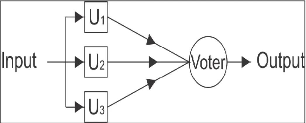
level, each individual component may be duplicated. If the failing transistors in an IC can be identified, the device can be redesigned for future use. However, since it is impossible to replace individual transistors in an IC of over 1 billion transistors, it is necessary to consider redundancy at a higher level. At a higher level, sub-circuits that house the faulty transistors may be replaced, as it is much easier to identity failing hardware modules. At the highest level, an entire system may be replaced; however this is a cost inefficient and is usually avoided. Triple modular redundancy (TMR), a widely used form of N-modular redundancy, involves triplicating a hardware module, typically a logic block, and feeding each of the three outputs into a voter circuit to produce a final output as shown in figure 13. A typical voter circuit such as figure 14 ensures that single bit errors are masked from the final output. For instance, if we assume that A is corrupted and flips from a correct value of 1 to a faulty value of 0, B and C should not be affected and should still have a value of 1, resulting in a final output value of 1. Multiple bit errors are also masked provided that they do not occur at the same node in the three circuits. TMR systems are very efficient and typically reduce SER rate to 0 so long as the voter circuit is heavily protected from radiation strikes, otherwise an error in the voter circuit will corrupt the final output. As with other logic repair and SER reduction techniques, TMR implementation introduces increased area (>200 %), speed, and power penalties.
Memory ICs can also implement robustness by having spare memory rows/columns that can be switched into a design to replace faulty memory rows/columns. It is usually more difficult to replace entire memory cells as a large design overhead is incurred, thus designers replace entire rows/columns. As memory blocks tend to have similar cells, it is exponentially easier to identify and replace faulty rows and columns in memory ICs than in combinational logic.
21
Figure 13: Triple Modular Redundancy
Figure 14: Voter Circuit
Due to the penalties associated with implementing logic repair and SER reduction techniques, it is imperative to provide designers with flexibility in selecting the protection level of ICs while balancing out design trade-offs. Furthermore, most of the currently available modi operandi for implementing hardware robustness apply to, or have been optimized for, memory elements, thereby presenting a dire need for strategies that target combinational logic. This thesis presents a technique that addresses the aforementioned issues by using approximate logic functions to take advantage of the logical masking effect discussed in Chapter II.
22
Figure 15: Conventional configuration for logic repair in digital circuits
23 CHAPTER IV
LOGIC REPAIR AND SER REDUCTION USING APPROXIMATE LOGIC FUNCTIONS
Combinational circuits are designed from Boolean functions which are made up of minterms/maxterms and represented by truth tables. Minterms represent product terms in which each of the input variables appear once, while maxterms represent sum terms in which each of the input variables appear once. Based on the corresponding minterms or maxterms, Boolean functions are minimized to reduce the overall area of the resulting combinational circuit implementation. This minimization is achieved using Karnaugh Maps (K-map). Essentially, when the input combinations represented by 2n minterms (or maxterms) are sufficiently close enough, meaning they only differ by 1 variable, the function can be minimized. When such a circuit is struck by radiation particles and produces a soft error in form of a bit flip in the final output, the original Boolean function represented by the combinational circuit changes, for as long as the error persists on the output.
Figure 16 illustrates such a scenario with a K-map representing a four-variable Boolean function.
(a) (b)
Figure 16: K-maps representing a Boolean function in (a) the original state (b) the error
24
corruption state with an upset minterm
The Boolean equation for the function represented in the K-map in figure 16(a) can be given as F = a’c’ + bc’d … (1) and it represents the original circuit in an unperturbed state. Assume a transistor in the circuit malfunctions due to a device level phenomenon or radiation particle strike modifying the output from logic 1 to logic 0 for one of the minterms. For instance, consider the case in figure 16(b) where the minterm abcd becomes faulty and changes from logic 0 to logic 1, the circuit implementation implements the Boolean equation in (2), which is radically dissimilar to the
F = a’c’ + abd … (2) original function and causes the circuit to malfunction, possibly affecting the entire system. FPGA designs are particularly susceptible to such errors, as they allow circuit implementations to be reprogrammed, thus a malfunction might be misjudged by the FPGA as a reprogramming.
Due to the perceived difficulty in repairing combinational circuits, research publications in the area of robustness are often deplete of strategies for combinational logic repair. Unlike memory ICs that are extensively composed of identical sub-blocks, combinational logic circuits rarely utilize similar blocks. Furthermore, any transistor in a circuit may be the cause of an IC failure, thus it is impossible to predict the type of failure that will occur. For instance, any of the minterms or maxterms in figure 16(b) that produce an output of logic 0 might become logic 1. As it is impossible to determine before-hand how many minterms will fail, many researchers assume that the likelihood of developing efficient logic repair strategies is low.
Single -Output Logic Repair
Fundamentally speaking, when an IC design experiences a fault, only the failing minterms
25
need to be replaced as the other unaffected minterms will continue to function properly unless they also encounter faults. Devising strategies to hinder failed minterm(s) from propagating to the final output of a design is paramount to efficient logic repair. As in the logical masking effect discussed in Chapter II, failed minterms can be prevented from corrupting the output of a design by desensitizing logical paths that correspond to the affiliated minterm. This is achievable by integrating logic repair circuits with the original design using novel hardware techniques. Therefore, once a failure is detected, the logic path from the transistor failure site to the output of the design needs to be desensitized and rerouted with a properly functioning path. TMR is an extreme form of logic repair via logical masking as it requires that the entire logic block be reproduced.
This approach enables designers to implement hardware robustness for combinational circuits, without having to replace entire logic blocks, by altering the intended path to output of the failed minterm and replacing it with a functionally accurate logical path that yields the correct output. This error detection and replacement method is achieved by adding extra detection and correction circuits whose sizes are largely dependent on the size of the original logic circuit. In a nutshell, this strategy is based on utilizing Boolean functions that represent under and over approximations of the original logic circuit. Considering the Venn diagram in figure 17 [3], assume that G is a function that represents a logic circuit and contains the entire input space for the combinational circuit, and that the rectangular box represents the entire input space and contains 2n set elements for n input variables. In this case, the area inside the G circle represents the input space for which the output of the original function is logic 1 (the members of this input space are the minterms for function G), and the area outside the G circle represents the input space for which the output of the original function is logic 0 (the members of this input space are the maxterms for function G). For this function G, the function F represents an under-approximation of G, and the
26
function H represents an over-approximation of G such that F ≤ G ≤ H. In other words, if an input vector 𝑥⃗ is a minterm of G, it must also be a minterm of H. Furthermore, any maxterm of H is also contained in G. This ensures that F only evaluates to 1 when G evaluates to 1, while H only evaluates to 0 when G evaluates to 0. By using strong F and H approximate functions, F and H will only differ from G for a small number of inputs. In a nutshell, approximate functions F and H are incomplete, additional sets of minterms and maxterms that can be used to replace any failing minterms/maxterms.
Figure 17 [3]: Over-approximation (H) and under-approximation (F) for an original function (G)
This strategy allows us to accurately assert the value of the minterms of G (based on the minterms of F), and the maxterms of G (based on the maxterms of H) ensuring that we can accurately determine the logic value of G. Even in the presence of an error on a minterm in G (as in a transistor failure in the original logic circuit that results in a 1 -> 0 output bit flip), F should contain a minterm that effectively logically masks out this error. Likewise, maxterms in H can be used to mask any maxterm errors in G. Under-approximation functions may be chosen from one of the large cubes that exist in the original design, while over-approximation functions may be chosen by
27
expanding a subset of minterms of the original design to form a larger cube. Since cubes contain fewer literals than original functions, using large cubes as approximate functions is an excellent way to minimize the area overhead of the additional logic repair circuitry. This will be discussed in more depth in Chapter V and corroborated with results in Chapter VI.
The effectiveness of the approximate functions used in masking errors is dependent on the number of minterms and maxterms F and H contain, thus if F and H contain most of the minterms and maxterms of G, then the failures in G can be tolerated more efficiently. In fact, failures only propagate to the output if F and H loosely bound G for the affected minterm or maxterm. Thus, for a protection circuit to be efficient, F U G and F U H must be very large sets. TMR is essentially an extreme example of this approach where approximate functions are strongest, guaranteeing that ever minterm/maxterm error will be masked. Weakening the approximations used in TMR decreases the associated penalties, while ensuring a reasonable amount of protection.
As in TMR, a decider circuit (voter circuit in TMR) is required to detect and correct errors masked by F and H. Figure 18 presents an and-or structure that essentially decides what the correct output should be.
Figure 18: And-Or decider circuit
F and H will mask any error in G provided that the affected minterm/maxterm is not an element in the set represented by the unmasked region shown in figure 17. Errors are unmasked only when F
28
evaluates to logic 0, G evaluates to logic 1, and H evaluates to logic 1. Based on the and-or structure in figure 18, when this happens, an error on node G that causes it to evaluate to logic 0 will result in an output of logic 0 which is considered an error as the correct value of G is a logic 1. Thus it is crucial to minimize the unmasked area as much as possible.
It is necessary to introduce a new term - repair coverage - to quantify what proportion of a logic circuit is covered against failures. In other words, a logic circuit will not have a repair-coverage of 100% unless all its minterms and maxterms are protected from errors. Considering the circuit represented in figure 16(a), we notice that the Boolean equations F = a’c’ and H = c (a’+b’) can be used as repair circuits. Since F covers 4 minterms of G, and H covers 10 maxterms of G, a total of 14 out of 16 minterms and maxterms are covered. The failed maxterm shown in figure 3 will be covered by H resulting in a correct output. This approach is more advantageous than the conventional block replacement strategy in figure 15 due to the flexibility provided to the designer. Typically, the strength of approximate functions F and H is also a function of area and power tradeoffs thus by slightly relaxing repair-coverage requirements, repair circuits of negligible area can be generated.
Thus, this approach can be applied to all functional blocks without overly compromising design tradeoffs.
Computing Repair-Coverage Factor
The repair capacity of a circuit, and the resulting complexity of F and H designs, depends on the coverage of G provided by F and H. As there are many approximate F and H functions for every given logic circuit, it is important to evaluate all these functions to choose the most appropriate approximation that will maximize repair coverage and minimize design penalties. Repair-Coverage is the premier factor for evaluating approximate functions. The repair-coverage factor is basically the
29
number of minterms and maxterms of G masked by F and H. ||F|| is a notation used to express the number of minterms of function F. F and 𝐻̅ are necessarily disjoint as illustrated by the gray regions in figure 17. Thus, the repair-coverage factor is the number of minterms contained in the gray portion divided by the entire input space represented by the rectangle, and is given by
γ =
(||𝐹||+||𝐻̅||)2n
.... (3) where n represents the number of variables/inputs. For example, if = 0.65, the approximate
functions can repair 65% of the possible minterms/maxterm failures. In the degenerate case of the strongest approximations, = 1 indicates that any failure is covered. However, the weakest approximation, = 0 indicates that no errors are masked and all failures propagate to the output. In real life fault injection experiments, the observed repair-coverage is likely to slightly different from the calculated estimate for several reasons. For one, radiation particle strikes can also impact F and H circuit implementations, thus they have to be accounted for. In this case, G becomes a repair circuit and since G represents the correct circuit implementation, the repair-coverage factor is slightly increased [3].
Multiple -Output Logic Repair
Since combinational logic blocks typical possess multiple outputs, or multi-bit outputs, it is important to modify the single-output logic repair strategy presented in the previous section for application in multiple-output logic blocks. Many of the techniques for logic repair fail to account for this and protect individual outputs selectively. However, for a combinational block to be considered fully protected from errors, every output needs to be protected for any input combination error. It is no use protecting one output and leaving the other output unprotected even if the protected output is more prone to soft errors. If the probability that the unprotected output produces a soft error
30
is non-zero, the overall vulnerability of the block increases. For this reason, it is important to protect outputs with respect to other outputs. Three methods are presented for application in multiple-output combinational blocks.
Non-Optimized Method
This is by far the crudest of the three methods to be explored. In essence, this method is an extrapolation of the single output repair technique. For each output, the single output technique is applied to generate F and H approximate functions. The F and H circuits can then be synthesized together to decrease the overall area increase. While this method is the easiest to implement, it is also the least effective for the following reasons. Assume that the two different outputs of the combinational block in figure 19 are represented by the K-maps in figure 20.
Figure 19: Black-box representation of a combinational circuit
Figure 20: K-maps representing two outputs of a logic block
31
The output functions can be split into minterm and maxterm functions and written as:
G(0)min = ac + cd’ + a’b’c, G(0)max = c (a+b’+d’) …. (4)
G(1)min = a’b’ + ab’d, G(1)max = b’ (a’+d) …. (5) Possible approximate functions for output G(0) and G(1) are given in figure 21 and 22 respectively.
F(0), seen in figure 21, provides protection for 4 minterms of G(0) - abcd, abcd’,
Figure 21: K-maps representing approximate functions for G(0)
ab’cd, and ab’cd’ - and is represented with the function F(0) = ac, while H(0) covers 8 maxterms of G(0) and is represented with the function H(0) = c. Thus, a total of 12 out of 16 minterms/maxterms are protected by F(0) and H(0), resulting in a repair-coverage factor of 0.75.
Figure 22: K-maps representing approximate functions for G(1)
32
The K-maps in figure 22 represent the approximate functions, F(1) and H(1), for the function G(1).
F(1) protects 4 of the 6 minterms of G(1) and can be represented by the equation F(1) = a’b’, while H(1) provides protection for 8 of 10 maxterms of G(1) and can be represented by the equation H(1)
= b’. Thus, a total of 12 out of 16 terms (minterm/maxterm) of G(1) are protected by F(1) and H(1), resulting in a repair-coverage factor of 0.75. Imagine that a fault occurs when the input abcd to the combinational block is 1001 (corresponds to minterm ab’c’d and maxterm (a’+b+c+d’)), propagates to both outputs G(0) and G(1), and causes G(0) to transition from 0 to 1 and G(1) to transition from 1 to 0. If this happens, H(0) provides adequate cover for G(0) and the error is masked from the output.
However, F(1) fails to mask this error from G(1) thus the fault propagates to the output as an error.
Therefore, even though G(0) is protected, G(1) is left exposed, resulting in a combinational block failure. This is the worst pitfall of this method.
For a combinational block to be immune to a certain term error, every output of the block has to mask the error. Thus, repair-coverage of the combinational block is estimated to be the product of the repair-coverage factors of the outputs. This implies that the overall repair-coverage of a logic block is less than the least of the per-output repair-coverage factors. This estimate used for determining the overall repair-coverage factor of a logic block is a tad inaccurate as it assumes that the term space set will be exhausted, whereas in real life, only a few term errors might occur. In addition, the repair-coverage factor of a block is very much dependent on the common protected terms between the approximate functions used for the outputs. For example, if the approximate functions of G(0) protect a certain term, and the approximate functions of G(1) also protect that term, then the combinational block is protected from that term error. This estimation formula is more accurate when the per-output repair-coverage factors are extremes, 0 or 1, and is slightly less accurate for non-extreme per-output repair-coverage factors. Despite the expected shortcomings of
33
this estimation formula, simulation results discussed in Chapter VI have proven that the formula is sufficient enough to serve as a baseline for quantifying the efficiency of the non-optimized method, as this method consistently underperforms the other two methods to be discussed. Based on the estimation formula, it can be implied that the repair-coverage factor is dependent on the number of outputs; an increase in the number of outputs results in a decrease in the repair-coverage of the logic block. Thus, the non-optimal method of logical masking is likely to be impractical for microprocessors and other IC blocks that often have multiple outputs and multiple-bit outputs.
Shared Minterm Method
To address the many issues that arise from the non-optimized method, it is essential to provide designers with other logic repair strategies that effectively utilize approximate functions.
One of such methods, the shared minterm method, requires collectively examining the multiple outputs of a logic block, to determine which outputs share minterms, and which of the possible shared minterm combinations is most appropriate for implementation. The basic idea behind this method is that outputs with shared minterms expose minterms that have to be protected. For example, consider the K-maps in figure 23.
Figure 23: Outputs of a logic block represented with K-maps
34
On the basis that cubes are used for approximate functions to reduce area, there are three major candidates for F(0) – a’b’, cd’, and ac -, and two major candidates for F(1) – a’b’, and ab’d. The cube a’b’ represents the shared minterms between G(0) and G(1). Thus, using the shared minterm method, F(0) = F(1) = a’b’. The benefit of picking the shared minterm cube as the approximate function for both outputs is quite obvious. If instead F(0) = cd’, and F(1) = a’b’, then errors that occur on G(0) and G(1) when a = 0 and b = 0 (minterm a’b’) will most likely cause a failure in the logic block. This is because for this input combination, G(1) will always be protected while G(0) will only be protected for 1 of the 4 possible input combinations, thus an error can occur 75% of the time even though the repair-coverage of G(0) does not change irrespective of which one of the three F(0) candidate functions is used. The repair-coverage of a block that utilizes this method cannot be lower than the percentage of terms masked by the shared minterms. Thus, this method is more beneficial for logic blocks with outputs that share many minterms.
There are some difficulties in implementing this method. The major stumbling block is the fact that brute-force search might be required to determine the best shared minterms to use. For a combinational block of n outputs, the time complexity of this algorithm is exponential - O(2n), as every possible output combination has to be considered. In general, (2n - n -1) combinations are examined for shared minterms. We subtract n and 1 from the total possible combination of 2n to eliminate the single outputs and no outputs “combinations” respectively. This exponential time complexity is very poor, especially for an application that is likely to have many outputs, therefore it is imperative to improve on this algorithm. This can be achieved by providing more hardware computation resources in the form of multi-processing units and multithreading the application program that implements this scheme. By dividing up the tasks into multiple processing units, the computation process can be speed up in accordance with Amdahl’s Law. The time complexity can
35
also be reduced by eliminating output combinations that are not expected to share any minterms based on previous computations. To achieve this, output combinations need to be processed in the order of least number of outputs. For instance, if a block has 5 outputs – a, b, c, d, e, 2-output- combinations should be examined first to determine if any of such combinations is sparse for shared minterms. If, for example, it is determined that the combination of outputs a and b produce 0 shared minterms, then 7 output combinations - abc, abd, abe, abcd, abce, abde, abcde – can be eliminated from the original set of 26 (25-5-1) output combinations. The number of eliminated output combinations is given by the equation:
¥ = 2(n-X) – 1 …. (6) Where n is the total number of outputs, and X is the number of outputs in the no-shared-minterm combination. We can verify equation (6) with the above example where ¥ = 2(5-2) – 1 = 7. The new equation for calculating the total number of output combinations is derived below:
Ȏ = 2n – n – 1 - ∑𝑛𝑘=2¥*vk – L [vk ≠ 0] …. (7) Ȏ = 2n – n – 1 - ∑𝑛𝑘=2(2𝑛−𝑘-1-m) vk – L [vk ≠ 0] …. (8) In the above equations, vk represents the number of distinct output combinations with vector size k that contain no shared minterms, m represents the number of output combinations that have been eliminated due to previously evaluated output combinations, and L represents the number of overlapping output combinations to be eliminated for output combinations with vector size k. This guarantees that for each k, the output combination eliminations will be distinct. Take the above example for instance. Assume that when k = 3, the output combination bcd was discovered to contain no shared minterms. Thus, 3 output combinations – bcd, abcd, abcde – are to be eliminated.
However, since abcd and abcde have already been eliminated, care must be taken to ensure that they are not double counted as output combinations can only be eliminated once.
36
By eliminating output combinations that are not expected to contain shared minterms, the computational time can be reduced drastically, provided that the minterms of the outputs are not strongly correlated. Nonetheless, while loose correlation might be good for area and computational time, it reduces the number of candidates that could be selected hereby essentially resulting in a lower repair-coverage factor. Also, additional memory requirements are imposed on a designer for storing the results of previous output combination evaluations. Additionally, the efficiency of output- combination-elimination decreases as the number of outputs increases.
After generating the shared minterms for every output combination, the most effective output combinations have to be decided upon. This is not a trivial affair as there are often many possibilities to choose from. Generally speaking, the ideal candidate for a given combinational block is any output combination that contains the most outputs and the most shared minterms. This ensures that the same output combination can be utilized for multiple outputs. Since ideal candidates rarely exist, output combinations that balance out the number of outputs they contain with the number of shared minterms they protect are usually chosen. The problem of determining which output combinations will produce the optimal solution is NP-hard. It should be noted that additional terms can be added to the shared minterm as this can slightly increase the repair-coverage factor at the expense of additional area.
Bestrc Method
An additional method was considered for logic repair to address the inadequacies of the first two methods. This method requires obtaining the best approximate functions (one F function and one H function), based on the single-output logic repair method, from the approximate functions chosen for each output. The same F and H functions are then used to determine which output terms will be
37
protected, such that when the output, from which the approximate functions were chosen, is protected from failures, the other outputs will also be protected. Consider a 4-input-3-output block with inputs a, b, c, d and outputs G(0), G(1), G(2) represented with the K-maps in figure 24.
Figure 24: K-maps for a 4-input-3-output combinational block
The best approximate functions for this combinational block, a.k.a. bestrc, is F(0) = a’b’ and H(0) = a, and is obtained from the output G(0) as it contains the most cubes. The next step is to guarantee that errors on other outputs will be masked for the terms covered by F and H, as shown in figure 25.
Figure 25: Approximate functions for G(1) and G(2) using bestrc method
38
The approximate functions for G(1) and G(2) are chosen by using the original function and replacing minterms/maxterms that are not covered by F(0) and H(0) with don’t care sets. The don’t- care terms can be replaced with cubes obtained from G(1) and G(2) or with any other logic values that aid the formation of large cubes.
This method is the often the most efficient in increasing the repair-coverage factor of combinational blocks, as it requires replicating most of the terms of the original function at the expense of increased area requirements. However, if the best approximate functions that are selected do not contain enough terms, the repair-coverage decreases. Nonetheless, this method is always better than the non-optimized methods, again at the expense of increased area. The overall repair- coverage factor of the block cannot be less than the repair-coverage factor of the bestrc.
In Chapter VII, the shared minterm and bestrc methods are combined to generate a theoretical optimal method.
39 CHAPTER V
IMPLEMENTATION OF THE APPROXIMATE LOGIC FUNCTIONS TECHNIQUE
Software programming is vital to logic repair as it speeds up the process of choosing and simulating repair circuits. Thus, for this project, a software tool was developed to assist in selecting and simulating the logic repair circuits generated from each of the three methods outlined in Chapter IV. This tool was written in C++, in a Linux environment, and it utilizes multiple freely available libraries for software development. The flowchart in figure 26 is a high-level representation of the implementation process.
Figure 26: Flow chart of Implementation Process
40
In summary, the software tool is invoked from the command line of a Linux/UNIX system and a programmable logic array (PLA) filename is encoded in the argument list that the tool receives. The pla file represented by the filename is then parsed to generate an appropriate software representation, and to populate the data structures used by the software program. After parsing the file, the program carries out certain manipulations (more data structure object declarations and populations, and output synthesis) on every output of the combinational block defined in the file.
Next, approximate functions are generated for each output based on any one of the three methods outlined in the previous chapter. Subsequently, the best approximate function is selected for each output, from the many possibilities, and synthesized with the original circuit to generate information about the overall area of the new circuit for the particular method. The above steps after output manipulation are repeated until all three methods have been exercised. After the best approximate functions have been selected for each method per output and synthesized to generate three new circuits (one for each method), fault simulation and analysis is performed on each of the three circuits to accurately quantify the actual repair-coverage factor and compare it with the theoretical repair-coverage proposed in Chapter IV. Finally, based on area, power, speed, and repair-coverage factor requirements, the designer must decide which of these three circuits is most appropriate for implementation in hardware. The subsequent sub-sections will provide an in-depth description of the input file format, the data structures used in representing combinational logic outputs, the strategy used by the computer program in selecting approximate functions from large cubes, and the fault simulation process.
Input File Format
Inputs files have to conform to the PLA format before they can be accepted by the logic tool.
![Figure 2 [29]: Particles deposited in the atmosphere after the impact of cosmic ray](https://thumb-ap.123doks.com/thumbv2/123dok/10740945.0/14.918.176.745.634.958/figure-29-particles-deposited-atmosphere-impact-cosmic-ray.webp)
![Figure 1 [28]: Flux of Cosmic Rays in Space](https://thumb-ap.123doks.com/thumbv2/123dok/10740945.0/14.918.111.809.148.531/figure-1-28-flux-cosmic-rays-space.webp)
![Figure 3 [28]: Particles deposited at sea level](https://thumb-ap.123doks.com/thumbv2/123dok/10740945.0/15.918.261.661.107.433/figure-3-28-particles-deposited-sea-level.webp)
![Figure 4 [4]: Charge generation per linear distance for some ions in Silicon](https://thumb-ap.123doks.com/thumbv2/123dok/10740945.0/17.918.302.674.396.629/figure-4-charge-generation-linear-distance-ions-silicon.webp)
![Figure 6 [6]: Charge collection and resulting transient current](https://thumb-ap.123doks.com/thumbv2/123dok/10740945.0/19.918.114.812.109.465/figure-6-6-charge-collection-resulting-transient-current.webp)
![Figure 8 [9]: Ion Strikes to the bit-line and storage cell of a 1T-DRAM](https://thumb-ap.123doks.com/thumbv2/123dok/10740945.0/20.918.329.595.783.1028/figure-ion-strikes-bit-line-storage-cell-dram.webp)
![Figure 9 [40]: Master-Slave D Flip-Flop arrangement](https://thumb-ap.123doks.com/thumbv2/123dok/10740945.0/21.918.114.815.522.791/figure-40-master-slave-d-flip-flop-arrangement.webp)
![Figure 11 [41]: Different SET masking effects](https://thumb-ap.123doks.com/thumbv2/123dok/10740945.0/22.918.141.782.470.822/figure-11-41-different-set-masking-effects.webp)
![Figure 12 [22]: Error rate dependence on frequency](https://thumb-ap.123doks.com/thumbv2/123dok/10740945.0/25.918.278.639.103.393/figure-12-22-error-rate-dependence-frequency.webp)