Thesis by Xiang Guan
In Partial Fulfillment of the Requirements for the degree of
Doctor of Philosophy
CALIFORNIA INSTITUTE OF TECHNOLOGY
Pasadena, California 2005
Defended September 22, 2005
© 2005
Xiang Guan
All Rights Reserved
Acknowledgement
First of all, I would like to express my sincere appreciation for my research advisor, Professor Ali Hajimiri, for his guidance and support over this five year journey. I would like to thank him for bringing me into the High-Speed Integrated Circuits Group at Caltech, where I have been able to work in my most favorite research field. Inspirations drawn from the fruitful and enlightening technical discussions with him have helped me overcome plenty of difficulties encountered in the design and experiments and have been crucial in making those projects successful. I am especially grateful for his constant encouragement, which will continue to promote my desire to do my best in my future career.
I would like to thank Professor David Rutledge and Dr. Sander Weinreb. I have learned a lot in the technical discussions with them. Their valuable suggestions as well as support in providing test equipments in the Caltech Microwave Laboratory have appreciably accelerated the progress of my research projects.
I feel very lucky to have worked with the current and previous members of Caltech High-Speed Integrated Circuits Group, Professor Hui Wu, Professor Donhee Ham, Professor Hossein Hashemi, Dr. Behnam Analui, Dr. Roberto Aparicio, Dr. Chris White, Arun Natarajan, Abbas Komijani, Jim Buckwalter, Ehsan Afshari, Ayding Babakhani, Yu-Jiu Wang, Hua Wang, Sam Mandegaran, Dr. Arjiang Hassibi, Dr. Ichiro Aoki, and Dr.
Scott Kee, each of whom gave me a lot of help in many aspects and made my time at Caltech enjoyable.
I also appreciate the help that I received from many other members of the Caltech
family, Dr. Dai Lu, Dr. Lawrence Cheung, Feiyu Wang, Guangxi Wang, Sanggeun Jeon,
Rumi Chunara, Naveed Neer-Ansari, Kent Potter, Niklas Wadefalk, Ann Shen, Michelle
Chen, Jim Endrizzi, and Victoria Lieding.
Special thanks to Professor Hossein Hashemi, my teammate in the project a 24-GHz integrated phased array receiver, which was accomplished via our seamless collaboration.
His jokes helped me get through the tough project with joy.
I would also like to acknowledge my teammates in designing the integrated 77-GHz transceiver: Adyin Babakhani, Arun Natarajan, Abbas Komijani and Yu-Jiu Wang.
I am thankful to the committee members in my candidacy exam: Professor David Rutledge, Professor Shuki Bruck, Professor Changhuei Yang, Dr. Sander Weinreb, and Professor Ali Hajimiri, each of whom gave me important and insightful feedback that opened my thoughts to new visual angles.
I wish to thank my Ph.D defense members: Prof. David Rutledge, Prof. Changhuei Yang, Dr. Sander Weinreb, and Dr. Larry D’Addario for their time.
Special thanks to my long-time friend, Hui Wu, who helped me adjust to life in the U.S. during my first year at Caltech.
I am profoundly grateful for my parents and my grandparents, who always love me, believe in me, and support me, no matter where I am.
Finally, I wish to express my appreciation for my wife, Yi Shen, whose unconditional
support and caring is an indispensable source of my strength.
Abstract
Microwave integrated systems in silicon provide a low cost, low power and high yield solution for wideband data communication, radar, and many other applications. Phased- array systems are capable of steering the radiation beam by electronic means, emulating the behavior of a directional antenna. This dissertation is dedicated to presenting various techniques to implement microwave integrated phased-array receivers in silicon-based technologies in the context of three design examples.
A 24-GHz 0.18-µm complementary metal oxide semiconductor (CMOS) front-end was demonstrated. The front-end consists of a low noise amplifier (LNA) and a mixer.
The LNA utilizes a novel topology common-gate with resistive feedthrough to obtain low-noise performance. The entire front-end achieves a 7.7dB noise figure and a 27.5dB power gain.
A fully integrated 8-element 24-GHz silicon germanium (SiGe) phased array receiver was implemented. The receiver uses two-step downconversion and local oscillator (LO) phase shifting with 4-bit resolution. The signal is combined at the 4.8-GHz intermediate frequency. The 16 phases of 19.2-GHz LO signal are generated with a voltage controlled oscillator (VCO) and symmetrically distributed to the phase selectors at all path.
Appropriate phase sequence is applied to the phase distribution transmission lines to minimize mismatch. An integrated frequency synthesizer locks the 19.2-GHz VCO output to a 75-MHz external reference. Measured array patterns show a peak-to-null ratio of more than 20dB and a beam steering range covering all signal incident angles.
An integrated 4-element 77-GHz SiGe wideband phased-array transceiver was
implemented. Two-step conversion is used at both the receiver and the transmitter. A
differential phase of 52 GHz is generated by the VCO and distributed to all RF paths at
the transmitter and receiver. The phase shifting is performed at the LO ports of the RF
mixers using continuous analog phase shifters. The quadrature signal of the second LO
frequency is generated by dividing the VCO frequency by a factor of 2 using a cross-
coupled injection-locked frequency divider. The signal combining is performed at IF with
an active combining amplifier. The receiver achieves a 41dB gain at 80 GHz with 3 GHz
of bandwidth. The 52-GHz-to-50MHz frequency divider chain obtains 7% locking range.
Contents
Acknowledgements iii
Abstract v
List of Figures xi
List of Tables xv
Chapter 1 Introduction 1
1.1 Organization...2
Chapter 2 Fundamentals of Single-Path and Multi-Path Receiver 4
2.1 Wireless Radio Reception...4
2.1.1 Noise ...4
2.1.1.1 Noise Sources In Circuits...5
2.1.1.2 Antenna Noise...7
2.1.1.3 Correlated And Uncorrelated Noise...7
2.1.1.4 Noise Factor ...8
2.1.1.5 Noise In Cascade System...9
2.1.1.6 Noise In Frequency Translation...9
2.1.2 Linearity...11
2.1.3 Dynamic Range...14
2.1.4 Single-Path Receiver Architecture...15
2.1.5 Frequency Synthesizer ...19
2.2 Phased Array Systems...21
2.2.1 Omnidirectional And Directional Communication...21
2.2.2 Operation Principles Of Phased Array Systems ...24
2.2.3 Spatial Filtering And Processing ...26
2.2.4 SNR Improvement ...28
2.2.5 Phased Array Architectures ...30
2.2.6 Applications ...34
2.2.7 Integrated Phased Array System In Silicon ...37
2.3 Chapter Summary ...38
Chapter 3 A 24-GHz CMOS Front-End 39
3.1 Introductions ...39
3.1.1 Motivations ...39
3.1.2 System Block Diagram ...40
3.2 Common-Gate With Resistive Feedthrough LNA...41
3.2.1 Basics of Twoport Noise Analysis...41
3.2.2 Noise Model of MOSFET...44
3.2.3 Noise Parameters of MOSFET ...45
3.2.4 Common-Source and Common-Gate LNA ...48
3.2.5 Common-Gate with Resistive Feedthrough (CGRF) LNA ...50
3.2.6 Noise Factor Optimization under Power Matching Constraints ....56
3.2.7....Stability...59
3.3 Circuits Implementation...61
3.3.1 Neutralizing Substrate Effects ...61
3.3.2 Schematics of the Front-End...62
3.3.3 Layout Issues ...64
3.4 Experimental Results ...65
3.5 Chapter Summary ...70
Appendix 3.1 Derivation of (3.54) to (3.59)...71
Appendix 3.2 Impacts of the Feedthrough Resistor on the Performance of a CG
Amplifier in Terms of NF, Gain, S
11and their Tradeoff ...74
Chapter 4 A Fully-Integrated 8-element 24-GHz Phased-array receiver in silicon 78
4.1 System Architecture...78
4.1.1 Top Level Block Diagram ...78
4.1.2 Array Pattern...80
4.2 Signal Path ...81
4.2.1 A 24-GHz SiGe Low Noise Amplifer ...81
4.2.1.1 Noise Model of SiGe Heterojunction Bipolar Transistor ..81
4.2.1.2 Noise Parameters of HBT ...82
4.2.1.3 Input Stage Design Procedure...83
4.2.1.4 LNA Implementation...84
4.2.1.5 Impedance Matching Network...86
4.2.2 A 24-GHz Downconverter and IF Combining Structure...87
4.2.3 IF Circuitry...92
4.2.4 Bandgap and PTAT References...93
4.3 Local Oscillator Path – PLL Design and Phase Generation ...96
4.3.1 PLL Basics ...96
4.3.2 Phase/Frequency Detector ...99
4.3.3 Charge Pump...102
4.3.4 Loop Filter ...104
4.3.5 VCO and Frequency Divider ...107
4.4 Local Oscillator Path – Phase Distribution...107
4.4.1 Binary Tree Structure...107
4.4.2 Coupling Effects of Two Parallel Transmission Lines ...108
4.4.3 EM Coupling inside a Transmission Line Array ...110
4.4.4 Transmission Line Properties in Various Phase Sequences ...112
4.5 Experimental Results ...115
4.5.1 Implementation ...115
4.5.2 Test Package ...118
4.5.3 Receiver Measurement Results...118
4.6 Chapter Summary ...128
Chapter 5 A 77-GHz Fully-Integrated Phased-Array Tranceiver 129
5.1 Introduction...129
5.2 System Architecture...131
5.3 Circuits Design...133
5.3.1 A 77-to-50-GHz Mixer ...133
5.3.2 A 26-GHz Two-Mode Amplifier ...135
5.3.3 A 26-GHz Signal Combining Amplifier...136
5.3.4 IF-to-Baseband Mixer and Buffer...139
5.3.5 A 52-GHz-to-50-MHz Frequency Divider Chain...140
5.4 Experimental Results ...145
5.5...Chapter Summary ...151
Chapter 6 Conclusion 152
6.1 Recommendations for Future Work...153
Bibliography 154
List of Figures
Figure 2.1: Resistor noise model (a) equivalent voltage (b) equivalent current...5
Figure 2.2: Antenna noise model ...7
Figure 2.3: Cascade system...9
Figure 2.4: Noise translation in a two-step downconversion receiver...10
Figure 2.5: Receiver linearity – single-tone test ...13
Figure 2.6: Receiver linearity – two-tone test...13
Figure 2.7: A generic superheterodyne receiver ...16
Figure 2.8: A generic homodyne receiver...18
Figure 2.9: LO spectrum and phase noise definition ...20
Figure 2.10: A PLL-based frequency synthesizer...21
Figure 2.11: Omnidirectional communication scheme...23
Figure 2.12: Directional communication scheme ...23
Figure 2.13: A generic phased-array architecture...25
Figure 2.14: Pattern of the array factor of an eight-element array with isotropic antenna elements and
d =λ/ 2...27
Figure 2.15: SNR improvement by the phased array...29
Figure 2.16: Passive RF phase shifting architecture...31
Figure 2.17: Active RF phase shifting architecture ...31
Figure 2.18: IF or baseband phase shifting architecture ...32
Figure 2.19: Digital phase shifting architecture...32
Figure 2.20: LO phase shifting architecture ...33
Figure 2.21: Automotive radar sensors provides multiple driving-aid functions ...36
Figure 3.1: Receiver block diagram...41
Figure 3.2: (a) A linear noisy twoport (b) An equivalent twoport ...42
Figure 3.3: Small-signal equivalent circuits of MOSFET ...44
Figure 3.4: Transistor configuration (a) common-source (b) common-gate ...46
Figure 3.5 LNA topologies (a) common-source with inductive degeneration (b) common- gate...48
Figure 3.6: Common-gate with resistive feedthrough LNA ...52
Figure 3.7: Small-signal circuits of CGRF stage ...52
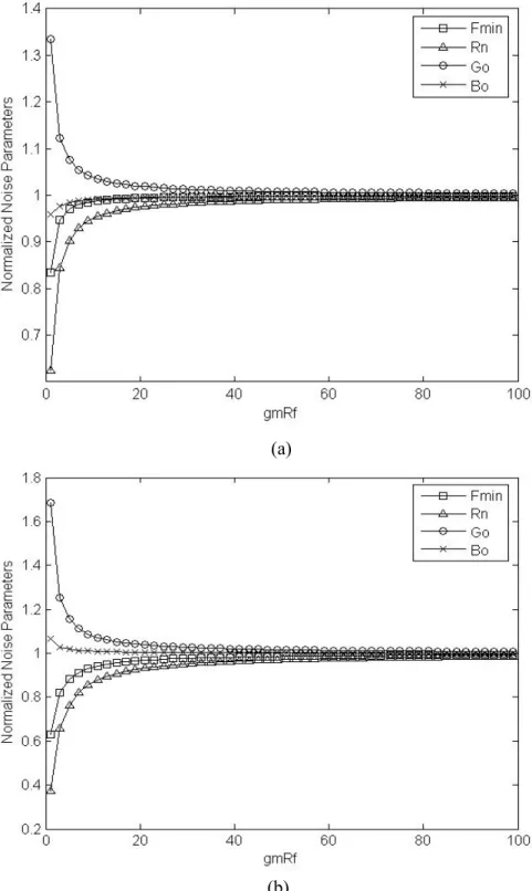
Figure 3.8: Normalized noise parameters as a function of
g Rm f(a)long channel (b) short channel ...54
Figure 3.9 Noise figure of CS and CGRF LNA under power matching constraints ...60
Figure 3.10: Two-port configuration ...61
Figure 3.11 Reducing substrate coupling by using parallel inductor...61
Figure 3.12: Three-stage LNA...63
Figure 3.13: Downconversion mixer ...63
Figure 3.14: Die micrograph of the 24GHz CMOS front-end...65
Figure 3.15: Input and output reflection coefficient ...67
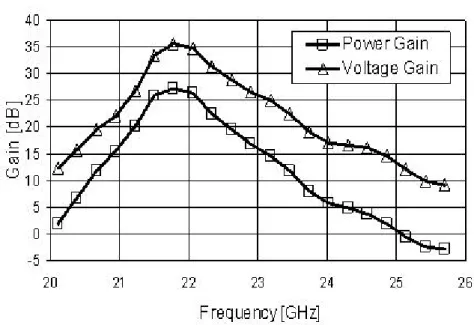
Figure 3.16: Voltage gain and power gain of the front-end...67
Figure 3.17: Large-signal nonlinearity ...68
Figure 3.18: Overall noise figure of the front-end...68
Figure 3.A.2.1: The NF of the CGRF LNA as a function of R
f(g
m=80mS, R
s=50Ω, and
RL=500Ω)...76
Figure 3.A.2.2: The G
Tof the CGRF LNA as a function of R
f(g
m=80mS, R
s=50Ω, and
RL=500Ω)...76
Figure 3.A.2.3: The G
Tof the CGRF LNA as a function of R
f(g
m=80mS, R
s=50Ω, and
RL=500Ω)...77
Figure 3.A.2.4: The S
11of the CGRF LNA as a function of R
f(g
m=80mS, R
s=50Ω, and
RL=500Ω)...77
Figure 4.1 System Architecture ...79
Figure 4.2: Array patterns of 16 different LO phase settings ...80
Figure 4.3: Small-signal and noise equivalent circuits of SiGe HBT...82
Figure 4.4: A 2-stage 24-GHz LNA ...84
Figure 4.5: Effects of bond pad and bond wire to LNA input impedance...85
Figure 4.6: LNA simulation results ...86
Figure 4.7: RF mixer and IF signal combining...88
Figure 4.8: A passive current combining structure...91
Figure 4.9: 4.8-GHz amplifier and mixer ...92
Figure 4.10: A bandgap and PTAT reference...93
Figure 4.11 Simulated result of bandgap reference (a) voltage reference (b) current reference...95
Figure 4.12: Block diagram of a generic charge pump PLL...98
Figure 4.13: Phase/frequency detector...99
Figure 4.14: Output waveforms of PFD (a)
ΔΦ ≠0(b)
ΔΦ =0...100
Figure 4.15: Implementation of DFF in Fig. 4.13...101
Figure 4.16: A generic charge pump...102
Figure 4.17: PFD and chargepump I/O waveforms when current mismatch exists ...103
Figure 4.18: A multi-switch charge pump ...104
Figure 4.19: Examples of the loop filter (a) single resistor (b) 1
st-order RC filter (c)2
nd- order RC filter ...105
Figure 4.20: 16-phase CMOS VCO...106
Figure 4.21: Phase distribution binary tree...107
Figure 4.22: Two coupled transmission lines (a) basic structure (b) lumped model...108
Figure 4.23: Transmission line arrays on silicon substrate...111
Figure 4.24: EM crosstalk inside a transmission line array...111
Figure 4.25: Three phase arrangements ...112
Figure 4.26: EM simulation results (a) transmission line impedance (b) amplitude
variations (c) phase variations ...114
Figure 4.27: Die Micrograph ...116
Figure 4.28: Test package 111...117
Figure 4.29: Phase-noise of free running VCO ...119
Figure: 4.30: PLL measurement results (a) Output Spectrum (b) Phase Noise...121
Figure 4.31: RF input reflection coefficient ...122
Figure 4.32: Single-path receiver gain...122
Figure 4.33: Two-tone measurement ...123
Figure 4.34 Gain compression ...123
Figure 4.35: Single-path noise figure...124
Figure 4.36: On-chip path-to-path isolation...124
Figure 4.37: Test setup for characterizing array performance...125
Figure 4.38: Normalized two-path array gain as a function of input phase difference at eight different LO settings ...126
Figure 4.39: Normalized four-path array gain as a function of incident angle at three different LO settings compared to theoretical results ...127
Figure 5.1: A fully-integrated 77-GHz phased-array transmitter-receiver ...132
Figure 5.2: 77-to-26-GHz Mixer...134
Figure 5.3 26-GHz two-gain mode amplifier ...136
Figure 5.4: A 26-GHz 4-element signal combining amplifier...138
Figure 5.5: 26-GHz-to-baseband mixer and 26-GHz LO buffer ...139
Figure 5.6: Baseband output buffer ...140
Figure 5.7: A digital frequency divider using emitter coupled logic DFF...141
Figure 5.8: Injection locked technique (a) A differential injection-locked frequency divider (b) A quadrature injection-locked frequency divider proposed in [106]...142
Figure 5.9: A cross-coupled quadrature frequency divider with output buffer ...143
Figure 5.10: Die Micrograph of 77-GHz Transmitter-Receiver...146
Figure 5.11: Receiver test setup...147
Figure 5.12: Divider chain sensitivity... 150
Figure 5.13: Receiver Gain...150
Figure 5.14: Receiver noise figure...151
List of Tables
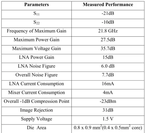
Table 3.1:Summary of the measurement performance of the 24-GHz 0.18µm-CMOS front-end...69 Table 3.2 LNA performance comparison ...69 Table 4.1 Summary of the measurement performance of the 24-GHz phased array
receiver...128
Table 5.1: Summary of the recent measurement performance of the 77-GHz phased-array
transceiver (the receiver and the frequency synthesizer parts) ...149
Chapter 1
Introduction
The demand for high-speed data communication motivates wireless system to operate at higher frequencies where larger bandwidth is available. According to Shannon’s theorem, the channel capacity (C) characterized by the highest data rate of reliable transmission in bits per second (bps), is given by [1]
log (12 / )
C= ×B +S N (1.1)
which indicates two fundamental factors setting the upper bound on the information transmission speed: the channel bandwidth B and the link signal-to-noise ratio (SNR) S/N. While the improvement of S/N is subject to various natural and implementation limitations, increasing B looks like a direct way to enhance achievable data-rate.
Wireless consumer applications utilizing the spectrum below 10 GHz have experienced explosive growth over the last decade, due to both the market demand and the advance of silicon-based technologies such as complementary metal-oxide semiconductor (CMOS) and silicon-germanium (SiGe) bipolar CMOS (BiCMOS) technologies, making low price and compact wireless mobile device a reality. One obstacle to utilize the frequency range above 10 GHz for wide-spread consumer applications is the high cost associate with current solutions using compound semiconductors, such as gallium arsenide (GaAs) and indium phosphide (InP).
Compared to compound semiconductor-based technologies, silicon-based technologies provide significant advantages in a higher level of integration on a single chip, thereby reducing cost and power dissipation. Today’s most advanced CMOS and SiGe BiCMOS processes offer transistors with transition and maximum oscillation frequency (fT, fmax) comparable to the compound semiconductor transistors [2], making possible the silicon-based integrated system and new applications using the microwave or millimeter-wave spectrum. Meanwhile, many new design
challenges have been introduced at such high frequencies due to the realities of silicon-based technologies such as lossy substrates, low breakdown voltages, low-Q passives, long interconnect parasitics, and high frequency coupling issues [3]. New design techniques need to be devised to deal with those problems.
One promising silicon-based microwave integrated system is a phased array transceiver. Phased arrays constitute a special class of multiple antenna systems that enable beam and null forming in various directions with electronic methods. This electronic steering makes it possible to take advantage of the antenna gain and directionality while eliminating the need for continuous mechanical reorientation of the antenna. Additionally, multiple-antenna systems alleviate the requirements for individual active devices used in the array and make the system more robust to individual component failure. Operating at high frequencies reduces the required element size and inter-element spacing in an antenna array.
This dissertation will present three works investigating the feasibly and performance of microwave and millimeter-wave integrated phased array receivers in silicon-based technologies. Various innovations developed along the way will be revealed in detail together with measurement verifications.
1.1 Organization
After reviewing the receiver fundamentals, the basic operations of phased array will be introduced in Chapter 2. We will then discuss the advantages, architectures, and applications of phased arrays in detail.
Chapter 3 will present our first step in this adventure, a 24-GHz CMOS front-end.
A novel low noise amplifier (LNA) topology, common-gate with resistive feedthrough (CGRF), is developed to obtain low-noise performance at an operation frequency comparable to fT.of the transistor. The advantages of this topology compared to traditional ones will be explained via thorough theoretical analysis.
Measurement results demonstrate the first 24-GHz 0.18-µm CMOS front-end with noise figure less than 8dB.
A fully integrated 8-element 24-GHz SiGe phased array receiver will be presented in Chapter 4. We will extensively address many aspects of this system, such as system architecture, a 24-GHz SiGe LNA, signal combining, a 19.2-GHz integrated PLL, multiphase distribution, a 24-GHz test setup, etc. Measurement results demonstrate the spatial selectivity and beam forming capability of the array as well a the high- performance receiver and frequency synthesizer.
In Chapter 5, we will describe a 77-GHz integrated SiGe wideband phased-array transceiver. The design, implementation, and measurement of the receiver signal path and a 52-GHz-to-25-MHz frequency divider chain will be presented where the important innovations include an active signal combining technique and a crossed- coupled quadrature injection-locked frequency divider. Finally, a summary of the highlights and some recommendations for future work will be given in Chapter 6.
Chapter 2
Fundamentals of Single-Path and Multi- Path Receiver
The objective of this chapter is to provide a theoretical foundation for discussions in the following chapters and a review of the existing technologies. The basic concepts in wireless radio reception and single-path receiver are reviewed in Section 2.1.
Section 2.2 describes the principles, advantages, and applications of phased array systems, the implementation of which is the main theme of this dissertation.
2.1 Wireless Radio Reception
Electromagnetic (EM) waves have been used to transmit information over air since Guglielmo Marconi invented the world’s first radio system in 1897. After more than one hundred years of evolution, the wireless communication systems have become tremendously complex, intelligent, and versatile. However, the essential obstacles for achieving fast and reliable information transmission remain the same: noise and interference.
2.1.1 Noise
In his essay On Noise, Arthur Schopenhauer wrote “Noise is a torture to all intellectual people.” Certainly circuit designers are among those suffering because we are constantly combating with electronic noise that blurs the signals and causes erroneous or even failed information transmission.
2.1.1.1 Noise Sources in Circuits
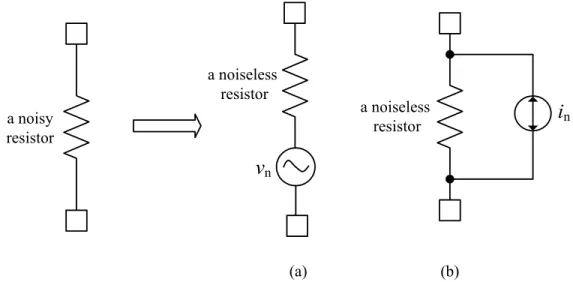
Noise in electronic systems arises from the random fluctuation in current flows and takes the form of thermal noise, shot noise, and flicker noise. Thermal noise originates from the random thermal motion of the carrier charges. The most common instance of thermal noise is resistor noise. If one measures the AC voltage across a resistor, a random voltage fluctuation of ( )v tn with zero mean and Gaussian amplitude distribution is observed. This noisy resistor can be represented with a noiseless resistor in series with a noise voltage source vn as shown in Figure 2.1 (a). Since
n( )
v t is a stationary random variable, it is characterized by its power spectrum density (PSD), which is given by
2( ) 4 v fn kTR
f =
∆ (2.1)
where R is the resistance value, T is the absolute temperature in Kelvin, k is Boltzmann’s constant equal to 1.38 10× −23Joules Kelvin/ . Equivalently, as shown in Figure 2.1 (b), the noisy resistor can be modeled by a noiseless resistor with a current noise generator in, whose PSD is given by
2( ) 4 i fn kT
f = R
∆ (2.2)
The maximum amount of noise power a resistor can pass to the load is delivered when
a noisy resistor
a noiseless resistor
v
na noiseless
resistor
i
n(a) (b)
Figure 2.1: Resistor noise model: (a) equivalent voltage (b) equivalent current
the load impedance is matched, which is given by
Pav =kBT (2.3)
where B is the noise bandwidth of the measurement. It is worth noticing that this available power is independent of the resistance value. In a receiving system the receiver input is often matched to the source impedance to get maximum signal power but also obtains the maximum noise power.
Equations (2.1) to (2.3) indicate that the resistor thermal noise has a flat spread spectrum, and hence is called white noise. In fact, resistor thermal noise does have a bandwidth that prevents infinite noise power. The -3dB bandwidth of the resistor thermal noise is on the order of 1 terahertz [4], therefore, in the frequency range of our interests, it can be treated as purely white. Thermal noise was first measured and clearly explained by Johnson [5] and Nyquist [6] in 1928, and therefore is referred to as Johnson noise or Nyquist noise. Thermal noise also exists in the conductance channel of a transistor such as field effect transistor (FET).
The current in a p-n junction barrier of a transistor or a diode is formed by discrete and independent carrier charges. Sampling the instantaneous number of charges crossing the junction with sensitive equipment, one can notice that it has a random variation with a Poisson distribution. This current variation is named shot noise, whose power spectrum is also white with power density [7]:
2( )
n 2
dc
i f f qI
∆ =
∆ (2.4)
where q is the electron charge (1.6 10× −19coulomb) and Idcis the direct current flowing through the junction. Unlike thermal noise, shot noise power density is independent of temperature.
Flicker noise is believed to be caused by the defects at the interface of different materials in a semiconductor device such as SiO2/Si interface in metal-oxide-silicon field effect transistor (MOSFET) and SiGe/Si interface in SiGe heterojunction bipolar transistor (HBT). These defects give rise to extra energy states that can randomly trap and release carrier charges, producing current variations. The power spectral density of the flicker noise is reversely proportional to the device size and frequency. Hence it is also called 1/f noise or pink noise. Due to its frequency dependence, flicker noise is
usually negligible in radio frequency (RF) circuits but can dominant the output noise power in baseband circuits up to a few hundred kilohertz.
2.1.1.2 Antenna Noise
An antenna at the receiver input not only picks up the desired signal carried by electromagnetic waves in air but also many forms of noise including broadband
“black body” radiations from all the objects in space. The total noise power collected by the antenna is an integral over its spatially selective receiving pattern and depends on the physical temperature of the black body objects.
The noise performance of the antenna is quantified by using the equivalent model shown in Figure 2.2 [4]. Va represents the signal collected by the antenna, Ra is a hypothetical resistance equal to the output impedance of the antenna, which is commonly 50Ω in wireless receiving system, and Tna is termed the antenna noise temperature, which is the absolute temperature at which Ra generates the same amount of noise power as the total noise power collected by the antenna. The available noise power from the antenna is given by
,
n av na
P =kBT (2.5)
2.1.1.3 Correlated and Uncorrelated Noise
The total output noise power of an electronic system is the summed effect of all noise sources. Unlike deterministic signals, which are simply treated with the superposition principle, the calculation of total noise power due to various noise sources is different.
Signals Noise
Va
Ra @ Tna
Figure 2.2: Antenna noise model
Considering two noise vectors X1 and X2, the average power of their summation is given by
2
1 2
( )
Psum = X + X (2.6)
=(X1+ X2)(X1*+X2*) (2.7)
= X12+ X22+X X1 2*+X X1* 2 (2.8) =PX1+PX2 +2 Re[ ]c P PX1. X2 (2.9) where c is termed correlation coefficient and defined as
1 2*
2 2
1 2
c X X X X
= (2.10)
which is a measure of the similarity of two random processes. If c=0, X1 and X2 are uncorrelated and the total noise power is the summation of the individual noise power of each noise source. If c=1, X1 and X2 are fully correlated. In other cases, X1 and X2
are partially correlated. Usually, the noises originated from independent physical sources are uncorrelated, such as the noise generated in different circuit components.
The noises generated by the same physical source can be fully or partially correlated, such as the channel noise and gate noise in a field effect transistor (FET). It is noteworthy that c can be a complex number if the correlation between two noise variables is related to their relative phases.
2.1.1.4 Noise Factor
The noise performance of the receiver is measured with noise factor (F) , defined at a specified frequency as the ratio of the output noise power per unit bandwidth to the output noise power engendered by the source [8]. In most wireless receiving systems, the source impedance is 50Ω and F is defined at the standard noise temperature To of 290K. The noise factor expressed in decibel form is called the noise figure (NF).
Assuming the antenna noise temperature is 290K at the input of a single path receiver, it can be derived that F is the ratio of the receiver’s signal-to-noise ratio (SNR) at the output to that at the input, which can be expressed in dB format as follows
, ,
out dB in dB
SNR =SNR −NF (2.11)
(2.11) indicates that NF represents the amount of SNR degraded after the signal is processed by the receiver. It is worth noting that in astronomic receivers, the antenna is pointed at much colder objects (or much hotter if it is looking at the sun), so the antenna noise temperature is much lower than 290K. In this case, the input/output SNR ratio is given by
1 ( 1)
in o
out na
SNR F T
SNR = + − T (2.12)
This ratio can be much higher than F if Tna To.
2.1.1.5 Noise in Cascade System
Consider one generic electronic system (Figure 2.3) composed of several blocks in cascade, i.e., the output of one stage feeds the input of the next. The ith stage exhibits an available power gain Gi and a noise factor Fi. Assuming that all stages are matched to the system characteristic impedance, the overall noise factor of the system is determined by the gain and noise factor of each stage via
2 3
1
1 1 2 1 2 3 1
1 1 ... 1
...
n n
F F F
F F
G G G G G G G −
− − −
= + + + + (2.13)
Equation (2.13) is known as Friis’s formula [9], which indicates that the noise factor of the first stage is most critical to the system noise performance because the noise due to each cascade stage is suppressed by the available power gain preceding it.
2.1.1.6 Noise in Frequency Translation
The receiver usually translates the radio-frequency (RF) signal to lower frequencies in order to facilitate signal processing. When frequency translation is involved, noise characterization is more complicated than in linear systems. To understand this, consider an ideal noiseless receiver using two separate LOs to downconvert RF signals to baseband via an intermediate frequency (IF) stage.
F1
G1
F2
G2
F3
G3
FN
GN
In Out
Figure 2.3: Cascade system
fLO1+fLO2+fBBfLO1+fLO2-fBBfLO1-fLO2-fBBfLO1fLO1-fLO2+fBBfLO2-fBBfLO2+fBBfLO2fBB
signalLO2LO1
RFIFBaseband Figure 2.5: Noise translation in a two-step downconversion receiverFigure 2.4: Noise translation in a two-step downconversion receiver
Assuming that no frequency selection is performed by the receiver and a unit conversion gain, at each step of the downconversion process, it is not only the noise at the signal band but also at the image band that is folded on top of the downconverted signal. Assuming that a single-tone RF signal resides at fLO1+ fLO2+ fBB, where
1
fLO and fLO2 are the first and second local oscillator (LO) frequency respectively, and fBB is the baseband frequency, as shown in Figure 2.4, the RF noise in four bands, given by fLO1+ fLO2+ fBB , fLO1+ fLO2− fBB , fLO1− fLO2+ fBB , and
1 2
LO LO BB
f − f − f , respectively, reaches fBB via the downconversion process.
Therefore, although the receiver itself is noiseless, the SNRout degrades by 6dB compared to SNRin. Moreover, the LO signal is often a strong signal at the frequency translation stage. Even if the LO signal is a pure single tone, it plays a role of square wave. Hence, the odd harmonics of fLOtranslate the noise at higher frequencies to signal band, further deteriorating the output SNR.
To clarify the confusion about the noise performance of a frequency translation system, two sets of definitions for noise factor are used. For the first definition, the source noise refers to those in the same frequency band of the signal only, which is called the single-side band (SSB) noise figure. For the second definition, the source noise refers to those in all the image bands and for a single frequency translation device, it is called double-side band noise figure (DSB). The SSB NF is always larger than the DSB NF, and the difference depends on the frequency selectivity of the receiver.
2.1.2 Linearity
Any unwanted signal fed into a receiver is called interference. Most interference comes from the signals intended for other users or other applications. The interference power can be orders of magnitude higher than the desired signal power and corrupt the signal if the linearity of the receiver is poor.
Any real receiver is a nonlinear system that responses linearly only if the input signal is sufficiently small. When the input signal increases beyond some extent, the nonlinear behaviors of the receiver become evident and are represented in gain compression and intermodulation products (IP) above noise floor.
One figure of merit for receiver linearity is the gain compression point.
Theoretically, the receiver’s output power increases linearly with the injected input power regardless of the input power level, as shown in Figure 2.5 [4] by the dashed line. The solid line in Figure 2.5 depicts a typical input/output transfer function of a real receiver. It can be seen that around Pin=0, the real I/O curve can be approximated with the straight line. As Pin increases, Pout gradually deviates from the linear curve and is eventually saturated. The point at which Pout is 1dB lower than its linear theoretical value is called the 1-dB compression point (CP1dB). The importance of this point is that it indicates where the receiver starts to leave the linear region and the intermodulation becomes serious problem. The receiver also generates spurs at the harmonics of the signal frequency when the gain goes into compression.
The most important specification of a receiver’s linearity is the third-order interception point. Consider two closely spaced interferences at f1 and f2 in the vicinity of signal band, where the strongest interference commonly originates. When the interference power is high enough, the receiver generates noticeable spurs at
1 2
nf mf
± ± due to intermodulation, where n and m are integers including zero. Two of these IPs, located at 2f1− f2 and 2f2− f1, are particularly threatening to the received signal because they can fall into the signal band and become impossible to eliminate by filtering. In general the power of the (n+m)th IP increases with a slope of (n+m)dB/1dB at the response to the increase of input interference power. Figure 2.6 shows the typical curves of the main tone and the third-order intermodulation power as a function of Pin. The third-order interception point is obtained by extrapolating the main-tone output at the slope of 1dB/1dB and the third-order IP curve at 3dB/1dB from the low input power level until they intersect with each other, as shown in Figure 2.6. The x-coordinate of the intersection point is called the input referred third-order interception point (IIP3), and the y-coordinate is called the output referred third-order interception point (OIP3).
In a cascaded system as shown in Figure 2.3, the overall IIP3 of the system is given by
1 1 2 1 2 3 1
3 3,1 3,2 3,3 3,
1 1 ...
... N
N
G G G G G G G
IIP IIP IIP IIP IIP
= + + + − (2.14)
1dB Pout
[dBm]
ICP1dB
Pin [dBm]
OCP1dB
Figure 2.5: Receiver linearity – single-tone test
Pout [dBm]
Pin [dBm]
Third order output 3:1 slope First order output
1:1 slope
(IIP3, OIP3)
Figure 2.6: Receiver linearity – two-tone test
It can be seen from (2.14) that in a cascade system the linearity requirements on the blocks at the back-end are more stringent because their effects on the overall system are “magnified” by the preceding gain.
2.1.3 Dynamic Range
Dynamic range (DR) is defined as the ratio of the maximum input power level that the circuit can tolerate to the minimum input power level that the circuits can properly detect [10]. DR specifies how well the system can handle signals with various power levels.
The lower bound of the dynamic range is set by the receiver sensitivity, defined as the lowest input signal power a receiver can appropriately process. To calculate the receiver sensitivity, one starts from the maximum bit error rate (BER) the data transmission can tolerate. To achieve this BER, the receiver must provide a minimum SNRout to the subsequent demodulator. Therefore, a minimum SNRin must be achieved at the receiver input, which is given by
,min, ,min,
in dB out dB
SNR =SNR +NF (2.15)
Assuming the receiver input is impedance matched to the antenna, the noise power delivered to the receiver is
,
n in na
P =kBT (2.16)
If the antenna noise temperature Tna is 290K, the receiver sensitivity can be obtained from (2.15) and (2.16) as
s,in,min,dBm 174dBm 10log( ) out,min,dB
P =NF− + B +SNR (2.17)
where -174dBm comes from 10log(KTo).
The upper limit of the dynamic range has various definitions that result in different bounds [4], but all are related to the linearity of the receiver. For instance, the most common definition, the spur-free dynamic range (SFDR), defines the maximum allowed input signal power as the one causing the minimum intermodulation product equal to the output noise power. From Figure 2.6, this input power level can be easily solved by using the graphical method, which is given by
,max, 3,
2 1( 174 10log )
3 3
in dBm dBm
P = IIP + NF− + B (2.18)
From (2.17) and (2.18), the receiver dynamic range can be found:
,max, 3, ,min,
2( 174 10log )
in dBm 3 dBm out dB
P = IIP −NF+ − B −SNR (2.19)
The receiving system often contains devices having adjustable gain at various stages. When the gain setting is changed, the dynamic range of the receiver is shifted up or down so that the overall dynamic range is improved, a process analogous to changing transmission gears in automobiles to provide a wide range of output speed.
2.1.4 Single-Path Receiver Architecture
In over one hundred years of development, many receiver architectures have been proposed and demonstrated for different requirements of various wireless applications.
The choice of receiver architecture considers performance, cost, complexity, power, integrity, and flexibility. A detailed discussion and comparison about each single-path architecture is beyond the scope of this dissertation and can be found in [10][11].
Here our discussion is focused on the two most common architectures, superheterodyne receiver and direct-conversion receiver, to show the general criteria and trade-offs at the system level.
Figure 2.7 depicts the block diagram of a generic heterodyne receiver [12]. The EM power picked up by the antenna is first pre-selected by an RF filter to reject the out-of-band interference and partially suppress the image signal. The RF filter must exhibit a low loss since it is directly added to the overall receiver noise figure. The LNA amplifies the signal power and provides the necessary gain for suppressing the noise of the subsequent blocks. An image rejecting filter is inserted between the LNA and the mixer to further attenuate the image interferences. The RF signal and its image are separated by 2fif in frequency domain. If fif is large enough, the RF filter and the tuned LNA may afford sufficient attenuation to the image, eliminating the need for IR filter. However, a high IF increases the quality factor requirement for the channel selection filter. Therefore, the choice of IF is a trade-off between channel selection and image rejection.
The mixer downconverts the RF signal to IF. The LO port of the mixer is usually driven by a frequency synthesizer that generates a tunable LO frequency. The receiver
RF filterLNA
A/D A/D
DSP0o 90oLO2 LO1
IR filterIF filterMixerVGA
Baseband filter Figure 2.7: A generic superheterodyne receiver
may need to cope with RF signals at different channels in a time-division fashion. A tunable LO translates RF signal at different channels to the same IF frequency so that a fixed channel selection filter can be used. A variable gain amplifier (VGA) prevents the subsequent circuits saturated by a large input. If DR of the input power is very high, a VGA can also be employed at the RF front-end and baseband to achieve more tuning capability.
Quadrature paths are often employed to translate the signal from IF to baseband, i.e., the LO signals driving the in-phase path (I path) mixer and quadrature path (Q path) mixer differ by 90o. This is because in the bandwidth-efficient modulation scheme, the signal spectrum is asymmetric around the carrier frequency. When downconverted to baseband, the information carried in the upper-side band will be irreversibly lost in those of the lower-side band. The solution to this problem is to separate the signal into two elements differing in phase and treat the two elements together as a complex variable, whose frequency spectrum is not necessarily symmetric to dc, so that the asymmetric information can be preserved.
The downconverted signal is further amplified, filtered, and transformed to the digital domain by using an analog-to-digital converter (ADC), from where much more complex and versatile functions can be performed by digital signal processing (DSP).
Because interference rejection and gain control can be performed at various stages of the downconversion path, the superheterodyne receiver achieves superior performance to other architectures with respect to selectivity, sensitivity, and dynamic range. Since being invented by Edwin Howard Armstrong in 1918 [13], the superheterodyne receiver has served the vast majority of the commercial wireless receivers to date.
The main drawback of the superheterodyne receiver is that when implemented in integrated circuits, it requires external IR and IF filters such as the surface acoustic wave (SAW) or ceramic filter, since the quality factor of integrated filters is limited by the substrate and ohmic loss. To drive the off-chip component via package parasitics, the LNA and mixer demand more power. Most importantly, more external components are used, lowering the cost efficiency of the whole system.
Two modified superheterodyne architectures have been proposed for integrated implementation: wideband-IF receiver [14] and low-IF receiver [15]. Both architectures choose to separate the signal to I and Q path at the first downconversion instead of the second downconversion, circumventing the image problem. However, the number of IF components is doubled, as well as the power consumption.
Figure 2.8 shows the block diagram of a direct-conversion receiver [16], also known as homodyne, or zero-IF, receiver. The direct-conversion receiver employs only one frequency translation step by setting the LO frequency equal to the RF carrier frequency. This architecture minimizes the number of external components by eliminating the IF stage and using quadrature path instead of IR filter to suppress images, hence it is more amenable to monolithic implementation than the superheterodyne receiver. A reduced number of building blocks and no off-chip components can lead to a low system power consumption. Due to those advantages, direct-conversion topology has been more and more popular in modern integrated communication systems.
However, to design a direct-conversion receiver one needs to carefully address several important problems which are less serious in the heterodyne receiver. One of those problems is LO-to-RF leakage. The LO power is leaked to the RF port through parasitic components, EM coupling or substrate, and mixes with the main LO tone, creating a DC offset, which is troublesome to remove in narrow-band modulation. For wideband modulation such as WCDMA, this DC offset is removed by using a base-
RF filter LNA
A/D
A/D 0o DSP
90o LO
Figure 2.8: A generic homodyne receiver
band high-pass filter with a low cut-off frequency, which has little impact on the signal quality. Another problem caused by LO-to-RF leakage is that the leaked LO signal can intermodulate with some strong interferences (for example, in WCDMA receivers, the powerful TX signal leaks into the receiver [17]) creating in-band distortions which are difficult to eliminate. I/Q mismatch is another serious consideration in a homodyne receiver. The phase and amplitude mismatches in the I and Q paths corrupt the signal by distorting the signal constellation. Although quadrature downconversion is also employed at the last downconversion stage in superheterodyne receiver, the I/Q mismatch is a less severe issue in this case because the low frequency mixer is less sensitive to parasitic mismatches. In addition, the direct-conversion receiver is more vulnerable to second order distortion and flicker noise in the circuits.
In short, there is no receiver architecture globally advantageous to all the others.
The optimum choice is determined under certain specifications and applications.
2.1.5 Frequency Synthesizer
A pure, accurate, stable, and tunable LO signal is another key factor for high performance communication system. The LO signal at gigahertz ranges is commonly generated by using a voltage controlled oscillator (VCO). However, the VCO output frequency has poor accuracy and varies with temperature. It has to be locked to a stable frequency source, such as a crystal temperature compensated oscillator, with a working frequency usually below 100MHz and frequency error below a few parts per million. The device that defines the relation of the output frequency to the reference frequency is called frequency synthesizer.
The frequency synthesizer has to achieve a sufficient tuning range and switching time as required by the specified communication system. Most importantly, it has to provide a pure output spectrum that most closely resembles an ideal impulse at the desired frequency, i.e., the spurs at the offset frequency should be low and the skirt around the main tone should be as narrow as possible. The quality of the main tone is quantified by phase noise. The frequency synthesizer output can be mathematically expressed as
( ) (v t = A A t+ n( ))cos(ωLOt+φn( ))t (2.20)
where A and ωLO are the amplitude and radian frequency of the main tone, respectively, and ( )A tn and ( )φn t are called amplitude noise and phase noise, respective, which represent the random disturbance at the output arising from the circuit and reference noise. Since the LO acts as a large signal at the switching device, an accurate zero-crossing time is critical to the receiver performance while it is insensitive to amplitude noise. Therefore, amplitude noise is not a significant concern in frequency synthesizer design. On the other hand, phase noise has to be minimized because it changes the zero-crossing time, downconverts nearby interferences into signal band, and integrates the noise around RF signal. The measure of phase noise is defined in the unit of dBc/Hz as the noise power per unit bandwidth at an offset ∆ω with respect to ωLO, normalized to the total carrier power under the spectrum, as shown in Figure 2.9 [18]. The phase noise specification is determined by the minimum signal-to-interference-plus-noise ratio (SINR) and the block level at the offset frequency.
In integrated implementation, the frequency synthesizer is often realized with a phase locked loop (PLL). If the output frequency is an integer multiple of the reference frequency, it is called an integer-N frequency synthesizer [19]. The integer- N frequency synthesizer has a simple configuration, as shown in Figure 2.10. The output frequency is adjusted by programming the frequency division ratio in the
c
ω
ω
1 Hzω
∆
dBc v
( )
S ω
Figure 2.9: LO spectrum and phase noise definition
feedback path. The main drawback of integer-N topology is that the resolution of the output frequency is limited to the reference source. Therefore, if a fine resolution is required, a high division ratio multiplies the reference phase noise at the output and a narrow bandwidth associated with low reference frequency increases the settling time.
This problem can be alleviated by using fractional-N architecture [20] where the output frequency can be varied at a fraction of the reference frequency. The architecture of the fractional-N synthesizer is similar to integer-N synthesizer, except that the divide-by-n frequency divider is replaced with a dual-modulus divide-by-n or divides-by-(n+1) frequency divider. By varying the percentage of time the frequency divider spends at the two divider values, the averaged VCO output frequency can be changed with a very fine granularity. Compared to the integer-N synthesizer, the fraction-N synthesizer can utilize a higher reference frequency, implying enhanced phase noise suppression and faster setting time. However, it requires a large scale of additional circuits to reduce spurious outputs at the fractional offset.
The design of the state-of-art PLL will be further elaborated upon in Chapter 4.
2.2 Phased Array Systems
2.2.1 Omnidirectional and Directional Communication
Omni-directional communication has been extensively used in various applications due to the insensitivity of orientation and location. Unfortunately, such systems suffer from several shortcomings [21]. As shown in Figure 2.11, the transmitter radiates electromagnetic power in all directions, and only a small fraction reaches the intended
Phase
Detector Z(s)
1/N fref, Fref VCO
fdiv, Fdiv
fout, Fout
Vcntl
Vpd
Figure 2.10: A PLL-based frequency synthesizer
receiver. Thus, for a given receiver sensitivity, a substantially higher power needs to be radiated by an omni-directional transmitter. Not only is a major fraction of this power wasted, but it also adds interference to other users. With dramatically expanding wireless applications and a rapidly enlarged number of users in each application, achievable data-rates in currently deployed wireless communication networks have become more interference-limited than noise-limited [22][23], wherein an increase in transmit power for all users enhances the interference level as well, producing no net benefit for the system capacity. Moreover, modern mobile stations such as cell phones or wireless LAN terminals are often serving in urban or office environments. The transmitted signal can be scattered by various objects such as terrain, walls, trees, vehicles, and people, creating multiple channel paths. The pockets of signal arriving at the receiver via different propagation paths are varied in amplitude and phase and can be added destructively. At certain points the receiver may receive zero signal even though the average transmitted signal power is high.
This effect is called “fading” in communication theory and is the primary reason why a cell phone losses a signal during a conversation [22]. Fading is an even more serious problem when moving into high frequencies, because when the receiver is moving it constantly passes the peaks and nulls of the fading effect; the distance between adjacent peak and null is proportional to the carrier wavelength. For instance, at 77GHz the wavelength in air is below half of a centimeter. To obtain reliable data transmission it is imperative for an omnidirectional receiver to be equipped with adaptive gain control and ultra-fast switching time, which is difficult to achieve. In addition, the multi-path propagation also causes inter-symbol interference (ISI), which further impairs the signal quality and limits the maximum achievable data rate.
Limited by the interference, fading, and delay spread, it has become more and more difficult to improve the system capacity per unit bandwidth in an omnidirectional communication scheme. Fortunately, such problems can be mitigated by utilizing space dimension in a directional communication, as shown in Figure 2.12.
In a directional communication system, power is only transmitted in the desirable direction(s) and is received from the intended source(s). This is commonly achieved by using directional antennas (e.g., a parabolic dish) that provide antenna gain for certain directions and attenuation in others. Due to the passive nature of the antenna and the conservation of energy, the antenna gain and its directionality go together; a
Figure 2.11: Omnidirectional communication scheme
Figure 2.12: Directional communication scheme
higher gain corresponds to a narrower beam width. Directional antennas are used when the relative location and orientation of neither the transmitter nor the receiver change quickly or frequently and are known in advance. For example, this is the case in fixed-point microwave links and satellite receivers. The additional antenna gain at the transmitter and/or receiver can substantially improve SINR and thereby increase the effective channel capacity. However, a single directional antenna is not well suited for portable applications, where its orientation needs to be changed quickly and constantly via mechanical means.
Fortunately, multiple antenna systems can be used to imitate a directional antenna whose bearing can be controlled electronically with no need for mechanical movement [24]-[29]. This electronic steering makes it possible to take advantage of the antenna gain and directionality while eliminating the need for continuous mechanical reorientation of the antenna. Additionally, multiple antenna systems alleviate the requirements for individual active devices used in the array and make the system more robust to individual component failure.
2.2.2 Operation Principles of Phased Array Systems
Multiple antenna systems can be employed on either the receive side (signal-input multiple-output: MIMO), the transmit side (multiple-input single-output: SIMO), or both ends (multiple-input multiple-output: MIMO) [30]. One type of multiple antenna system is to utilize antenna space diversity to create an independent channel path and combine the received signal in an optimum way using space-time processing [23][31][32]. The algorithm and implementation of a MIMO system based on this principle has intrigued a large volume of research and industrial effort in last decade.
This technique is easy to implement in the base station of a mobile communication system [33]. However, such a system is not favorable for a mobile unit since it requires the antenna separation on the order of a magnitude higher than the wavelength to obtain a low channel correlation coefficient, and a comparatively higher power due to little hardware shared [34], which conflicts with the compact and low-power requirements of the mobile devices.
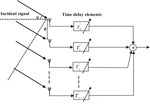
The phased array is a special type of multiple antenna system. A phased array receiver consists of several signal paths, each connected to a separate antenna. Generally, radiated signal arrives at spatially-separated antenna elements at different times. An ideal phased-array compensates the time delay difference between the elements and combines the signals coherently to enhance the reception from the desired direction(s) while rejecting emissions from other directions. We will use a one-dimensional n- element linear array as an example to illustrate the principle as shown in Figure 2.13.
We will discuss only the receiver case in this paper, but similar concepts are applicable to the transmitter due to reciprocity.
For a plane wave, the signal arrives at each antenna element with a progressive time delay τ at each antenna. This delay difference between two adjacent elements is related to their distance (d) and the signal angle of incidence with respect to the normal, θ, by
θ τ dsin
c = (2.21)
where c is the speed of light. In general, the signal arriving at the first antenna element is given by
0( ) ( ) cos[ c ( )]
S t = A t ωt+ϕ t (2.22)
θ d
+
Incident signal Time delay elements
'
τ
0'
τ
2'
−1
τ
n'
τ
1Figure 2.13: A generic phased-array architecture
where A(t) and φ(t) are the amplitude and phase of the signal and ωc is the carrier frequency. The signal received by the kth element can be expressed as
( ) 0( ) ( ) cos[ ( )]
k c c
S t =S t k− τ =A t k− τ ωt k− ω τ ϕ+ t k− τ (2.23) The equal spacing of the antenna elements is reflected in (2.23) as a progressive phase
difference ωcτ and a progressive time delay τ in A(t) and φ(t). Adjustable time delay elements (τn') can compensate the signal delay and phase difference simultaneously, as shown in Figure 2.13. The combined signal Ssum(t) can be expressed as
1 1
' ' ' '
0 0
( ) ( ) ( ) cos[ ( )]
n n
sum k k k c c k c k
k n
S t − S t τ − A t kτ τ ωt ω τ kω τ ϕ t kτ τ
= =
=
∑
− =∑
− − − − + − − (2.24)Forτk' =−kτ the total output power signal is given by:
( )Ssum t =nA t( ) cos[ωct+ϕ( )]t (2.25)
The most straightforward way to obtain this time delay is by using broadband adjustable delay elements in the RF path. However, adjustable time delays at RF are challenging to integrate due to many non-ideal effects such as loss, noise, and nonlinearity. While an ideal delay can compensate the arrival time differences at all frequencies, in narrowband applications it can be approximated via other means. For a narrow band signal, A(t) and φ(t) change slowly relative to the carrier frequency, i.e., when τ <<τmodulatewe have
) ( )
(t A t kτ
A ≈ − (2.26)
) ( )
( ϕ τ
ϕ t ≈ t−k (2.27)
Therefore, we only need to compensate for the progressive phase difference ωcτ in (2.23). The time delay element can be replaced by a phase shifter which provides a phase-shift of φkto the kth path. To add the signal coherently, φkshould be given by
k k c
φ
=ω τ
(2.28)Unlike the wideband case, phase compensation for the narrowband signal can be made at various locations in the receiving chain, i.e., RF, LO, IF, analog baseband, or digital domain.
2.2.3 Spatial Filtering and Processing
One important advantage of a phased-array is its ability to significantly attenuate the incident interference power from other directions, even by using omnidirectional
antenna elements. The received or radiated pattern of an array is obtained by multiplying the received pattern of a single antenna element by an array factor, assuming identical current distribution in each antenna element. The array factor for a linea