P ART O NE
P
art One provides a background and context for the remainder of this book.This part presents the fundamental concepts of computer architecture and operating system internals.
ROAD MAP FOR PART ONE
Chapter 1 Computer System Overview
An operating system mediates among application programs, utilities, and users, on the one hand, and the computer system hardware on the other. To appreciate the functionality of the operating system and the design issues involved, one must have some appreciation for computer organization and architecture. Chapter 1 provides a brief survey of the processor, memory, and Input/Output (I/O) elements of a com- puter system.
Chapter 2 Operating System Overview
The topic of operating system (OS) design covers a huge territory, and it is easy to get lost in the details and lose the context of a discussion of a particular issue.
Chapter 2 provides an overview to which the reader can return at any point in the book for context. We begin with a statement of the objectives and functions of an operating system. Then some historically important systems and OS functions are described. This discussion allows us to present some fundamental OS design princi- ples in a simple environment so that the relationship among various OS functions is clear. The chapter next highlights important characteristics of modern operating sys- tems. Throughout the book, as various topics are discussed, it is necessary to talk about both fundamental, well-established principles as well as more recent innova- tions in OS design. The discussion in this chapter alerts the reader to this blend of established and recent design approaches that must be addressed. Finally, we pre- sent an overview of Windows, UNIX, and Linux; this discussion establishes the gen- eral architecture of these systems, providing context for the detailed discussions to follow.
Background
6
C OMPUTER S YSTEM O VERVIEW
1.1 Basic Elements 1.2 Processor Registers
User-Visible Registers Control and Status Registers 1.3 Instruction Execution
Instruction Fetch and Execute I/O Function
1.4 Interrupts
Interrupts and the Instruction Cycle Interrupt Processing
Multiple Interrupts Multiprogramming 1.5 The Memory Hierarchy 1.6 Cache Memory
Motivation Cache Principles Cache Design
1.7 I/O Communication Techniques Programmed I/O
Interrupt-Driven I/O Direct Memory Access
1.8 Recommended Reading and Web Sites 1.9 Key Terms, Review Questions, and Problems
APPENDIX 1A Performance Characteristicd of Two-Level Memories Locality
Operation of Two-Level Memory Performance
APPENDIX 1B Procedure Control Stack Implementation Procedure Calls and Returns Reentrant Procedures
7
CHAPTER
An operating system (OS) exploits the hardware resources of one or more processors to provide a set of services to system users. The OS also manages secondary memory and I/O (input/output) devices on behalf of its users. Accordingly, it is important to have some understanding of the underlying computer system hardware before we begin our examination of operating systems.
This chapter provides an overview of computer system hardware. In most areas, the survey is brief, as it is assumed that the reader is familiar with this subject. However, several areas are covered in some detail because of their importance to topics covered later in the book.
1.1 BASIC ELEMENTS
At a top level, a computer consists of processor, memory, and I/O components, with one or more modules of each type. These components are interconnected in some fashion to achieve the main function of the computer, which is to execute programs.
Thus, there are four main structural elements:
• Processor: Controls the operation of the computer and performs its data pro- cessing functions. When there is only one processor, it is often referred to as the central processing unit (CPU).
• Main memory: Stores data and programs. This memory is typically volatile;
that is, when the computer is shut down, the contents of the memory are lost.
In contrast, the contents of disk memory are retained even when the computer system is shut down. Main memory is also referred to as real memory or primary memory.
• I/O modules: Move data between the computer and its external environ- ment. The external environment consists of a variety of devices, including secondary memory devices (e. g., disks), communications equipment, and terminals.
• System bus: Provides for communication among processors, main memory, and I/O modules.
Figure 1.1 depicts these top-level components. One of the processor’s func- tions is to exchange data with memory. For this purpose, it typically makes use of two internal (to the processor) registers: a memory address register (MAR), which specifies the address in memory for the next read or write; and a memory buffer reg- ister (MBR), which contains the data to be written into memory or which receives the data read from memory. Similarly, an I/O address register (I/OAR) specifies a particular I/O device. An I/O buffer register (I/OBR) is used for the exchange of data between an I/O module and the processor.
A memory module consists of a set of locations, defined by sequentially num- bered addresses. Each location contains a bit pattern that can be interpreted as ei- ther an instruction or data. An I/O module transfers data from external devices to processor and memory, and vice versa. It contains internal buffers for temporarily holding data until they can be sent on.
1.2 PROCESSOR REGISTERS
A processor includes a set of registers that provide memory that is faster and smaller than main memory. Processor registers serve two functions:
• User-visible registers: Enable the machine or assembly language programmer to minimize main memory references by optimizing register use. For high- level languages, an optimizing compiler will attempt to make intelligent choices of which variables to assign to registers and which to main memory locations. Some high-level languages, such as C, allow the programmer to sug- gest to the compiler which variables should be held in registers.
• Control and status registers: Used by the processor to control the operation of the processor and by privileged OS routines to control the execution of programs.
Figure 1.1 Computer Components: Top-Level View
CPU Main memory
System bus
I/O module
Buffers
Instruction
n⫺2 n⫺1 Data
Data Data Data Instruction Instruction
PC ⫽ Program counter IR ⫽ Instruction register MAR ⫽ Memory address register MBR ⫽ Memory buffer register I/O AR ⫽ Input/output address register I/O BR ⫽ Input/output buffer register
0 1 2
PC MAR
IR MBR
I/O AR I/O BR
Execution unit
There is not a clean separation of registers into these two categories. For example, on some processors, the program counter is user visible, but on many it is not. For purposes of the following discussion, however, it is convenient to use these categories.
User-Visible Registers
A user-visible register may be referenced by means of the machine language that the processor executes and is generally available to all programs, including application programs as well as system programs. Types of registers that are typically available are data, address, and condition code registers.
Data registers can be assigned to a variety of functions by the programmer. In some cases, they are general purpose in nature and can be used with any machine in- struction that performs operations on data. Often, however, there are restrictions.
For example, there may be dedicated registers for floating-point operations and oth- ers for integer operations.
Address registers contain main memory addresses of data and instructions, or they contain a portion of the address that is used in the calculation of the complete or effective address. These registers may themselves be general purpose, or may be devoted to a particular way, or mode, of addressing memory. Examples include the following:
• Index register: Indexed addressing is a common mode of addressing that in- volves adding an index to a base value to get the effective address.
• Segment pointer: With segmented addressing, memory is divided into segments, which are variable-length blocks of words.1A memory reference consists of a reference to a particular segment and an offset within the segment; this mode of addressing is important in our discussion of memory management in Chapter 7.
In this mode of addressing, a register is used to hold the base address (starting location) of the segment. There may be multiple registers; for example, one for the OS (i.e., when OS code is executing on the processor) and one for the cur- rently executing application.
• Stack pointer: If there is user-visible stack2addressing, then there is a dedi- cated register that points to the top of the stack. This allows the use of instruc- tions that contain no address field, such as push and pop.
For some processors, a procedure call will result in automatic saving of all user- visible registers, to be restored on return. Saving and restoring is performed by the processor as part of the execution of the call and return instructions. This allows each
1There is no universal definition of the term word. In general, a word is an ordered set of bytes or bits that is the normal unit in which information may be stored, transmitted, or operated on within a given com- puter. Typically, if a processor has a fixed-length instruction set, then the instruction length equals the word length.
2A stack is located in main memory and is a sequential set of locations that are referenced similarly to a physical stack of papers, by putting on and taking away from the top. See Appendix 1B for a discussion of stack processing.
procedure to use these registers independently. On other processors, the program- mer must save the contents of the relevant user-visible registers prior to a procedure call, by including instructions for this purpose in the program. Thus, the saving and restoring functions may be performed in either hardware or software, depending on the processor.
Control and Status Registers
A variety of processor registers are employed to control the operation of the processor. On most processors, most of these are not visible to the user. Some of them may be accessible by machine instructions executed in what is referred to as a control or kernel mode.
Of course, different processors will have different register organizations and use different terminology. We provide here a reasonably complete list of register types, with a brief description. In addition to the MAR, MBR, I/OAR, and I/OBR registers mentioned earlier (Figure 1.1), the following are essential to instruction execution:
• Program counter (PC): Contains the address of the next instruction to be fetched
• Instruction register (IR): Contains the instruction most recently fetched All processor designs also include a register or set of registers, often known as the program status word (PSW), that contains status information. The PSW typically contains condition codes plus other status information, such as an interrupt enable/disable bit and a kernel/user mode bit.
Condition codes (also referred to as flags) are bits typically set by the proces- sor hardware as the result of operations. For example, an arithmetic operation may produce a positive, negative, zero, or overflow result. In addition to the result itself being stored in a register or memory, a condition code is also set following the exe- cution of the arithmetic instruction. The condition code may subsequently be tested as part of a conditional branch operation. Condition code bits are collected into one or more registers. Usually, they form part of a control register. Generally, machine instructions allow these bits to be read by implicit reference, but they cannot be al- tered by explicit reference because they are intended for feedback regarding the re- sults of instruction execution.
In processors with multiple types of interrupts, a set of interrupt registers may be provided, with one pointer to each interrupt-handling routine. If a stack is used to implement certain functions (e. g., procedure call), then a stack pointer is needed (see Appendix 1B). Memory management hardware, discussed in Chapter 7, requires dedicated registers. Finally, registers may be used in the control of I/O operations.
A number of factors go into the design of the control and status register orga- nization. One key issue is OS support. Certain types of control information are of specific utility to the OS. If the processor designer has a functional understanding of the OS to be used, then the register organization can be designed to provide hardware support for particular features such as memory protection and switching between user programs.
Another key design decision is the allocation of control information between registers and memory. It is common to dedicate the first (lowest) few hundred or thousand words of memory for control purposes. The designer must decide how much control information should be in more expensive, faster registers and how much in less expensive, slower main memory.
1.3 INSTRUCTION EXECUTION
A program to be executed by a processor consists of a set of instructions stored in memory. In its simplest form, instruction processing consists of two steps: The processor reads (fetches) instructions from memory one at a time and executes each instruction. Program execution consists of repeating the process of instruction fetch and instruction execution. Instruction execution may involve several operations and depends on the nature of the instruction.
The processing required for a single instruction is called an instruction cycle.
Using a simplified two-step description, the instruction cycle is depicted in Figure 1.2.
The two steps are referred to as the fetch stage and the execute stage. Program execu- tion halts only if the processor is turned off, some sort of unrecoverable error occurs, or a program instruction that halts the processor is encountered.
Instruction Fetch and Execute
At the beginning of each instruction cycle, the processor fetches an instruction from memory. Typically, the program counter (PC) holds the address of the next instruc- tion to be fetched. Unless instructed otherwise, the processor always increments the PC after each instruction fetch so that it will fetch the next instruction in sequence (i.e., the instruction located at the next higher memory address). For example, con- sider a simplified computer in which each instruction occupies one 16-bit word of memory. Assume that the program counter is set to location 300. The processor will next fetch the instruction at location 300. On succeeding instruction cycles, it will fetch instructions from locations 301, 302, 303, and so on. This sequence may be al- tered, as explained subsequently.
The fetched instruction is loaded into the instruction register (IR). The in- struction contains bits that specify the action the processor is to take. The processor interprets the instruction and performs the required action. In general, these actions fall into four categories:
• Processor-memory: Data may be transferred from processor to memory or from memory to processor.
Figure 1.2 Basic Instruction Cycle
START Fetch next HALT
instruction
Fetch stage Execute stage
Execute instruction
• Processor-I/O: Data may be transferred to or from a peripheral device by transferring between the processor and an I/O module.
• Data processing: The processor may perform some arithmetic or logic opera- tion on data.
• Control: An instruction may specify that the sequence of execution be altered.
For example, the processor may fetch an instruction from location 149, which specifies that the next instruction be from location 182. The processor sets the program counter to 182. Thus, on the next fetch stage, the instruction will be fetched from location 182 rather than 150.
An instruction’s execution may involve a combination of these actions.
Consider a simple example using a hypothetical processor that includes the characteristics listed in Figure 1.3. The processor contains a single data register, called the accumulator (AC). Both instructions and data are 16 bits long, and memory is organized as a sequence of 16-bit words. The instruction format pro- vides 4 bits for the opcode, allowing as many as 2416 different opcodes (repre- sented by a single hexadecimal3 digit). The opcode defines the operation the processor is to perform. With the remaining 12 bits of the instruction format, up to 2124096 (4 K) words of memory (denoted by three hexadecimal digits) can be directly addressed.
0 3 4 15
15
Opcode Address
0 1
S Magnitude
Program counter (PC) = Address of instruction Instruction register (IR) = Instruction being executed Accumulator (AC) = Temporary storage
(a) Instruction format
(b) Integer format
(c) Internal CPU registers
0001 = Load AC from memory 0010 = Store AC to memory 0101 = Add to AC from memory
(d) Partial list of opcodes Figure 1.3 Characteristics of a Hypothetical Machine
3A basic refresher on number systems (decimal, binary, hexadecimal) can be found at the Computer Sci- ence Student Resource Site at WilliamStallings. com/StudentSupport.html.
Figure 1.4 illustrates a partial program execution, showing the relevant por- tions of memory and processor registers. The program fragment shown adds the contents of the memory word at address 940 to the contents of the memory word at address 941 and stores the result in the latter location. Three instructions, which can be described as three fetch and three execute stages, are required:
1. The PC contains 300, the address of the first instruction. This instruction (the value 1940 in hexadecimal) is loaded into the IR and the PC is incremented.
Note that this process involves the use of a memory address register (MAR) and a memory buffer register (MBR). For simplicity, these intermediate registers are not shown.
2. The first 4 bits (first hexadecimal digit) in the IR indicate that the AC is to be loaded from memory. The remaining 12 bits (three hexadecimal digits) specify the address, which is 940.
3. The next instruction (5941) is fetched from location 301 and the PC is incremented.
4. The old contents of the AC and the contents of location 941 are added and the result is stored in the AC.
5. The next instruction (2941) is fetched from location 302 and the PC is incremented.
6. The contents of the AC are stored in location 941.
2 PC 300
CPU registers Memory
Fetch stage Execute stage
3 0 0 1 9 4 0
301 5 9 4 1 302 2 9 4 1 940 0 0 0 3 941 0 0 0 2
AC 1 9 4 0 IR
Step 1
PC 300
CPU registers Memory
3 0 1 1 9 4 0
301 5 9 4 1 302 2 9 4 1 940 0 0 0 3 941 0 0 0 2
AC 1 9 4 0 IR 0 0 0 3
Step 2 PC
300
CPU registers Memory
3 0 1
0 0 0 5
0 0 0 5 0 0 0 3
0 0 0 5 1 9 4 0
301 5 9 4 1 302 2 9 4 1 940 0 0 0 3 941 0 0 0 2
AC 5 9 4 1 IR
Step 3
PC 300
CPU registers Memory
3 0 2 1 9 4 0
301 5 9 4 1 302 2 9 4 1 1 940 0 0 0 3 941 0 0 0 2
AC 5 9 4 1 IR
Step 4 PC
300
CPU registers Memory
3 0 1 9 4 0
301 5 9 4 1 302 2 9 4 1 940 0 0 0 3 941 0 0 0 2
AC 2 9 4 1 IR
Step 5
PC 300
CPU registers Memory
3 0 3 1 9 4 0
301 5 9 4 1 302 2 9 4 1 940 0 0 0 3 941 0 0 0 5
AC 2 9 4 1 IR
Step 6
3 + 2 = 5
Figure 1.4 Example of Program Execution (contents of memory and registers in hexadecimal)
In this example, three instruction cycles, each consisting of a fetch stage and an execute stage, are needed to add the contents of location 940 to the contents of 941.
With a more complex set of instructions, fewer instruction cycles would be needed.
Most modern processors include instructions that contain more than one address.
Thus the execution stage for a particular instruction may involve more than one ref- erence to memory. Also, instead of memory references, an instruction may specify an I/O operation.
I/O Function
Data can be exchanged directly between an I/O module (e. g., a disk controller) and the processor. Just as the processor can initiate a read or write with memory, speci- fying the address of a memory location, the processor can also read data from or write data to an I/O module. In this latter case, the processor identifies a specific de- vice that is controlled by a particular I/O module. Thus, an instruction sequence sim- ilar in form to that of Figure 1.4 could occur, with I/O instructions rather than memory-referencing instructions.
In some cases, it is desirable to allow I/O exchanges to occur directly with main memory to relieve the processor of the I/O task. In such a case, the processor grants to an I/O module the authority to read from or write to memory, so that the I/O- memory transfer can occur without tying up the processor. During such a transfer, the I/O module issues read or write commands to memory, relieving the processor of responsibility for the exchange. This operation, known as direct memory access (DMA), is examined later in this chapter.
1.4 INTERRUPTS
Virtually all computers provide a mechanism by which other modules (I/O, memory) may interrupt the normal sequencing of the processor. Table 1.1 lists the most com- mon classes of interrupts.
Interrupts are provided primarily as a way to improve processor utilization.
For example, most I/O devices are much slower than the processor. Suppose that the processor is transferring data to a printer using the instruction cycle scheme of Figure 1.2. After each write operation, the processor must pause and remain idle
Table 1.1 Classes of Interrupts
Program Generated by some condition that occurs as a result of an instruction execution, such as arithmetic overflow, division by zero, attempt to execute an illegal machine instruction, and reference outside a user’s allowed memory space.
Timer Generated by a timer within the processor. This allows the operating system to perform certain functions on a regular basis.
I/O Generated by an I/O controller, to signal normal completion of an operation or to signal a variety of error conditions.
Hardware failure Generated by a failure, such as power failure or memory parity error.
until the printer catches up. The length of this pause may be on the order of many thousands or even millions of instruction cycles. Clearly, this is a very wasteful use of the processor.
To give a specific example, consider a PC that operates at 1 GHz, which would allow roughly 109instructions per second.4A typical hard disk has a rotational speed of 7200 revolutions per minute for a half-track rotation time of 4 ms, which is 4 million times slower than the processor.
Figure 1.5a illustrates this state of affairs. The user program performs a series of WRITE calls interleaved with processing. The solid vertical lines represent seg- ments of code in a program. Code segments 1, 2, and 3 refer to sequences of instruc- tions that do not involve I/O. The WRITE calls are to an I/O routine that is a system utility and that will perform the actual I/O operation. The I/O program consists of three sections:
• A sequence of instructions, labeled 4 in the figure, to prepare for the actual I/O operation. This may include copying the data to be output into a special buffer and preparing the parameters for a device command.
• The actual I/O command. Without the use of interrupts, once this command is issued, the program must wait for the I/O device to perform the requested
User program
WRITE
WRITE
WRITE
I/O program
I/O Command
END 1
2
3
2
3 4
5
(a) No interrupts
User program
WRITE
WRITE
WRITE
I/O program
I/O Command
Interrupt handler
END 1
2a
2b
3a
3b
4
5
(b) Interrupts; short I/O wait
User program
WRITE
WRITE
WRITE
I/O program
I/O Command
Interrupt handler
END
1 4
5
(c) Interrupts; long I/O wait Figure 1.5 Program Flow of Control without and with Interrupts
4A discussion of the uses of numerical prefixes, such as giga and tera, is contained in a supporting docu- ment at the Computer Science Student Resource Site at WilliamStallings. com/StudentSupport.html.
function (or periodically check the status, or poll, the I/O device). The program might wait by simply repeatedly performing a test operation to determine if the I/O operation is done.
• A sequence of instructions, labeled 5 in the figure, to complete the operation.
This may include setting a flag indicating the success or failure of the operation.
The dashed line represents the path of execution followed by the processor; that is, this line shows the sequence in which instructions are executed. Thus, after the first WRITE instruction is encountered, the user program is interrupted and execution continues with the I/O program. After the I/O program execution is complete, execu- tion resumes in the user program immediately following the WRITE instruction.
Because the I/O operation may take a relatively long time to complete, the I/O program is hung up waiting for the operation to complete; hence, the user program is stopped at the point of the WRITE call for some considerable period of time.
Interrupts and the Instruction Cycle
With interrupts, the processor can be engaged in executing other instructions while an I/O operation is in progress. Consider the flow of control in Figure 1.5b.
As before, the user program reaches a point at which it makes a system call in the form of a WRITE call. The I/O program that is invoked in this case consists only of the preparation code and the actual I/O command. After these few instructions have been executed, control returns to the user program. Meanwhile, the external device is busy accepting data from computer memory and printing it. This I/O op- eration is conducted concurrently with the execution of instructions in the user program.
When the external device becomes ready to be serviced, that is, when it is ready to accept more data from the processor, the I/O module for that external de- vice sends an interrupt request signal to the processor. The processor responds by suspending operation of the current program; branching off to a routine to service that particular I/O device, known as an interrupt handler; and resuming the original execution after the device is serviced. The points at which such interrupts occur are indicated by in Figure 1.5b. Note that an interrupt can occur at any point in the main program, not just at one specific instruction.
For the user program, an interrupt suspends the normal sequence of execu- tion. When the interrupt processing is completed, execution resumes (Figure 1.6).
Thus, the user program does not have to contain any special code to accommodate interrupts; the processor and the OS are responsible for suspending the user pro- gram and then resuming it at the same point.
To accommodate interrupts, an interrupt stage is added to the instruction cycle, as shown in Figure 1.7 (compare Figure 1.2). In the interrupt stage, the processor checks to see if any interrupts have occurred, indicated by the presence of an interrupt signal. If no interrupts are pending, the processor proceeds to the fetch stage and fetches the next instruction of the current program. If an interrupt is pending, the processor suspends execution of the current program and executes an interrupt-handler routine. The interrupt-handler routine is generally part of the OS. Typically, this routine determines the nature of the interrupt and performs
whatever actions are needed. In the example we have been using, the handler de- termines which I/O module generated the interrupt and may branch to a program that will write more data out to that I/O module. When the interrupt-handler rou- tine is completed, the processor can resume execution of the user program at the point of interruption.
It is clear that there is some overhead involved in this process. Extra instructions must be executed (in the interrupt handler) to determine the nature of the interrupt and to decide on the appropriate action. Nevertheless, because of the relatively large amount of time that would be wasted by simply waiting on an I/O operation, the processor can be employed much more efficiently with the use of interrupts.
Fetch stage Execute stage Interrupt stage
START
HALT Interrupts
disabled
Interrupts enabled Fetch next
instruction
Execute instruction
Check for interrupt;
initiate interrupt handler
Figure 1.7 Instruction Cycle with Interrupts 1
2
i i 1
M Interrupt
occurs here
User program Interrupt handler
Figure 1.6 Transfer of Control via Interrupts
To appreciate the gain in efficiency, consider Figure 1.8, which is a timing dia- gram based on the flow of control in Figures 1.5 a and 1.5b. Figures 1.5b and 1.8 as- sume that the time required for the I/O operation is relatively short: less than the time to complete the execution of instructions between write operations in the user program. The more typical case, especially for a slow device such as a printer, is that the I/O operation will take much more time than executing a sequence of user in- structions. Figure 1.5 c indicates this state of affairs. In this case, the user program reaches the second WRITE call before the I/O operation spawned by the first call is complete. The result is that the user program is hung up at that point. When the pre- ceding I/O operation is completed, this new WRITE call may be processed, and a new I/O operation may be started. Figure 1.9 shows the timing for this situation with and without the use of interrupts. We can see that there is still a gain in efficiency be- cause part of the time during which the I/O operation is underway overlaps with the execution of user instructions.
4
Processor wait
Processor wait
1
5 5
2
5
3 4
Time
I/O operation
I/O operation
I/O operation
I/O operation
4 2a
1
2b 4 3a 5 3b
(a) Without interrupts (circled numbers refer to numbers in Figure 1.5a)
(b) With interrupts (circled numbers refer to numbers in Figure 1.5b)
Figure 1.8 Program Timing: Short I/O Wait
Interrupt Processing
An interrupt triggers a number of events, both in the processor hardware and in software. Figure 1.10 shows a typical sequence. When an I/O device completes an I/O operation, the following sequence of hardware events occurs:
1. The device issues an interrupt signal to the processor.
2. The processor finishes execution of the current instruction before responding to the interrupt, as indicated in Figure 1.7.
3. The processor tests for a pending interrupt request, determines that there is one, and sends an acknowledgment signal to the device that issued the interrupt. The acknowledgment allows the device to remove its interrupt signal.
Processor wait
Processor wait
Processor wait
(a) Without interrupts (circled numbers refer to numbers in Figure 1.5a)
(b) With interrupts (circled numbers refer to numbers in Figure 1.5c)
Processor wait
4 1
5
2
5
3 4
4
2 1
5 4
3
5
I/O operation
I/O operation
I/O operation
I/O operation Time
Figure 1.9 Program Timing: Long I/O Wait
4. The processor next needs to prepare to transfer control to the interrupt routine.
To begin, it saves information needed to resume the current program at the point of interrupt. The minimum information required is the program status word (PSW) and the location of the next instruction to be executed, which is contained in the program counter.These can be pushed onto a control stack (see Appendix 1B).
5. The processor then loads the program counter with the entry location of the interrupt-handling routine that will respond to this interrupt. Depending on the computer architecture and OS design, there may be a single program, one for each type of interrupt, or one for each device and each type of inter- rupt. If there is more than one interrupt-handling routine, the processor must determine which one to invoke. This information may have been in- cluded in the original interrupt signal, or the processor may have to issue a request to the device that issued the interrupt to get a response that contains the needed information.
Once the program counter has been loaded, the processor proceeds to the next instruction cycle, which begins with an instruction fetch. Because the instruction fetch is determined by the contents of the program counter, control is transferred to
Device controller or other system hardware issues an interrupt
Processor finishes execution of current instruction
Processor signals acknowledgment of interrupt
Processor pushes PSW and PC onto control stack
Processor loads new PC value based on interrupt
Save remainder of process state information
Process interrupt
Restore process state information
Restore old PSW and PC
Hardware Software
Figure 1.10 Simple Interrupt Processing
the interrupt-handler program. The execution of this program results in the following operations:
6. At this point, the program counter and PSW relating to the interrupted pro- gram have been saved on the control stack. However, there is other informa- tion that is considered part of the state of the executing program. In particular, the contents of the processor registers need to be saved, because these registers may be used by the interrupt handler. So all of these values, plus any other state information, need to be saved. Typically, the interrupt handler will begin by saving the contents of all registers on the stack. Other state information that must be saved is discussed in Chapter 3. Figure 1.11 a shows a simple example. In this case, a user program is interrupted after the instruction at location N. The contents of all of the registers plus the address of the next instruction (N + 1), a total of M words, are pushed onto the control stack. The stack pointer is updated to point to the new top of stack, and the program counter is updated to point to the beginning of the interrupt service routine.
7. The interrupt handler may now proceed to process the interrupt.This includes an examination of status information relating to the I/O operation or other event that caused an interrupt. It may also involve sending additional commands or ac- knowledgments to the I/O device.
8. When interrupt processing is complete, the saved register values are retrieved from the stack and restored to the registers (e. g., see Figure 1.11b).
9. The final act is to restore the PSW and program counter values from the stack.
As a result, the next instruction to be executed will be from the previously inter- rupted program.
It is important to save all of the state information about the interrupted pro- gram for later resumption. This is because the interrupt is not a routine called from the program. Rather, the interrupt can occur at any time and therefore at any point in the execution of a user program. Its occurrence is unpredictable.
Multiple Interrupts
So far, we have discussed the occurrence of a single interrupt. Suppose, however, that one or more interrupts can occur while an interrupt is being processed. For example, a program may be receiving data from a communications line and printing results at the same time. The printer will generate an interrupt every time that it completes a print operation. The communication line controller will generate an interrupt every time a unit of data arrives. The unit could either be a single character or a block, depending on the nature of the communications discipline. In any case, it is possible for a commu- nications interrupt to occur while a printer interrupt is being processed.
Two approaches can be taken to dealing with multiple interrupts. The first is to disable interrupts while an interrupt is being processed. A disabled interrupt simply means that the processor ignores any new interrupt request signal. If an interrupt occurs during this time, it generally remains pending and will be checked by the processor after the processor has reenabled interrupts. Thus, when a user program is executing and an interrupt occurs, interrupts are disabled immediately. After the
interrupt-handler routine completes, interrupts are reenabled before resuming the user program, and the processor checks to see if additional interrupts have oc- curred. This approach is simple, as interrupts are handled in strict sequential order (Figure 1.12a).
The drawback to the preceding approach is that it does not take into account relative priority or time-critical needs. For example, when input arrives from the communications line, it may need to be absorbed rapidly to make room for more input. If the first batch of input has not been processed before the second batch ar- rives, data may be lost because the buffer on the I/O device may fill and overflow.
Start
N 1 Y L
N Y
Y
T
Return
User's program
Main memory
Processor
General registers Program counter
Stack pointer
N + 1 T M
T M T Control
stack
Interrupt service routine
User's program Interrupt service routine
(a) Interrupt occurs after instruction at location N
(b) Return from interrupt
Start
N 1 Y L
N Y T
Return
Main memory
Processor
General registers Program counter
Stack pointer
Y L 1
T M
T M
T Control
stack
N 1
Figure 1.11 Changes in Memory and Registers for an Interrupt
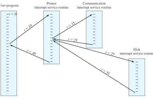
A second approach is to define priorities for interrupts and to allow an interrupt of higher priority to cause a lower-priority interrupt handler to be interrupted (Figure 1.12b). As an example of this second approach, consider a system with three I/O de- vices: a printer, a disk, and a communications line, with increasing priorities of 2, 4, and 5, respectively. Figure 1.13, based on an example in [TANE06], illustrates a possible se- quence.A user program begins at t0.At t10, a printer interrupt occurs; user infor- mation is placed on the control stack and execution continues at the printer interrupt service routine (ISR). While this routine is still executing, at t15 a communications interrupt occurs. Because the communications line has higher priority than the printer, the interrupt request is honored. The printer ISR is interrupted, its state is pushed onto the stack, and execution continues at the communications ISR.While this
User program
Interrupt handler X
Interrupt handler Y
(a) Sequential interrupt processing
(b) Nested interrupt processing User program
Interrupt handler X
Interrupt handler Y
Figure 1.12 Transfer of Control with Multiple Interrupts
routine is executing, a disk interrupt occurs (t20). Because this interrupt is of lower priority, it is simply held, and the communications ISR runs to completion.
When the communications ISR is complete (t 25), the previous processor state is restored, which is the execution of the printer ISR. However, before even a single instruction in that routine can be executed, the processor honors the higher- priority disk interrupt and transfers control to the disk ISR. Only when that routine is complete (t35) is the printer ISR resumed. When that routine completes (t40), control finally returns to the user program.
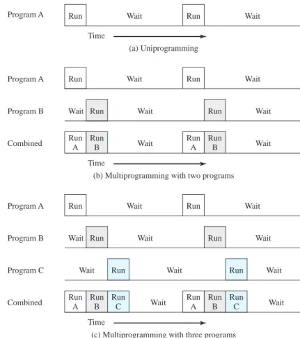
Multiprogramming
Even with the use of interrupts, a processor may not be used very efficiently. For example, refer to Figure 1.9b, which demonstrates utilization of the processor with long I/O waits. If the time required to complete an I/O operation is much greater than the user code between I/O calls (a common situation), then the processor will be idle much of the time. A solution to this problem is to allow multiple user pro- grams to be active at the same time.
Suppose, for example, that the processor has two programs to execute. One is a program for reading data from memory and putting it out on an external device;
the other is an application that involves a lot of calculation. The processor can begin the output program, issue a write command to the external device, and then proceed to begin execution of the other application. When the processor is dealing with a number of programs, the sequence with which programs are executed will depend on their relative priority as well as whether they are waiting for I/O. When a pro- gram has been interrupted and control transfers to an interrupt handler, once the in- terrupt-handler routine has completed, control may not necessarily immediately be returned to the user program that was in execution at the time. Instead, control may
User program Printer
interrupt service routine
Communication interrupt service routine
Disk interrupt service routine
t10
t40
t15
t25
t25
t35
t 0
Figure 1.13 Example Time Sequence of Multiple Interrupts
pass to some other pending program with a higher priority. Eventually, the user pro- gram that was interrupted will be resumed, when it has the highest priority. This con- cept of multiple programs taking turns in execution is known as multiprogramming and is discussed further in Chapter 2.
1.5 THE MEMORY HIERARCHY
The design constraints on a computer’s memory can be summed up by three ques- tions: How much? How fast? How expensive?
The question of how much is somewhat open ended. If the capacity is there, applications will likely be developed to use it. The question of how fast is, in a sense, easier to answer. To achieve greatest performance, the memory must be able to keep up with the processor. That is, as the processor is executing instructions, we would not want it to have to pause waiting for instructions or operands. The final question must also be considered. For a practical system, the cost of memory must be reason- able in relationship to other components.
As might be expected, there is a tradeoff among the three key characteristics of memory: namely, capacity, access time, and cost. A variety of technologies are used to implement memory systems, and across this spectrum of technologies, the following relationships hold:
• Faster access time, greater cost per bit
• Greater capacity, smaller cost per bit
• Greater capacity, slower access speed
The dilemma facing the designer is clear. The designer would like to use mem- ory technologies that provide for large-capacity memory, both because the capacity is needed and because the cost per bit is low. However, to meet performance re- quirements, the designer needs to use expensive, relatively lower-capacity memories with fast access times.
The way out of this dilemma is to not rely on a single memory component or technology, but to employ a memory hierarchy. A typical hierarchy is illustrated in Figure 1.14. As one goes down the hierarchy, the following occur:
a. Decreasing cost per bit b. Increasing capacity
c. Increasing access time
d. Decreasing frequency of access to the memory by the processor
Thus, smaller, more expensive, faster memories are supplemented by larger, cheaper, slower memories. The key to the success of this organization decreasing frequency of access at lower levels. We will examine this concept in greater detail later in this chapter, when we discuss the cache, and when we discuss virtual memory later in this book. A brief explanation is provided at this point.
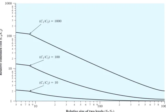
Suppose that the processor has access to two levels of memory. Level 1 con- tains 1000 bytes and has an access time of 0.1 µs; level 2 contains 100,000 bytes and has an access time of 1 µs. Assume that if a byte to be accessed is in level 1, then the
processor accesses it directly. If it is in level 2, then the byte is first transferred to level 1 and then accessed by the processor. For simplicity, we ignore the time required for the processor to determine whether the byte is in level 1 or level 2. Figure 1.15 shows the general shape of the curve that models this situation.The figure shows the average access time to a two-level memory as a function of the hit ratio H, where H is defined as the fraction of all memory accesses that are found in the faster memory (e. g., the cache), T1is the access time to level 1, and T2is the access time to level 2.5As can be seen, for high percentages of level 1 access, the average total access time is much closer to that of level 1 than that of level 2.
In our example, suppose 95% of the memory accesses are found in the cache (H⫽0.95). Then the average time to access a byte can be expressed as
(0.95) (0.1 µs) ⫹(0.05) (0.1 µs ⫹1 µs) ⫽0.095 ⫹0.055 ⫽0.15 µs
5If the accessed word is found in the faster memory, that is defined as a hit. A miss occurs if the accessed word is not found in the faster memory.
Inboard memory
Outboard storage
Off-line storage
Main memory
Magnetic disk CD-ROM CD-R
W DVD-R W DVD-RAM
Magnetic tape Cache
Reg- isters
Figure 1.14 The Memory Hierarchy
The result is close to the access time of the faster memory. So the strategy of using two memory levels works in principle, but only if conditions (a) through (d) in the preceding list apply. By employing a variety of technologies, a spectrum of mem- ory systems exists that satisfies conditions (a) through (c). Fortunately, condition (d) is also generally valid.
The basis for the validity of condition (d) is a principle known as locality of ref- erence [DENN68]. During the course of execution of a program, memory references by the processor, for both instructions and data, tend to cluster. Programs typically contain a number of iterative loops and subroutines. Once a loop or subroutine is en- tered, there are repeated references to a small set of instructions. Similarly, opera- tions on tables and arrays involve access to a clustered set of data bytes. Over a long period of time, the clusters in use change, but over a short period of time, the proces- sor is primarily working with fixed clusters of memory references.
Accordingly, it is possible to organize data across the hierarchy such that the percentage of accesses to each successively lower level is substantially less than that of the level above. Consider the two-level example already presented. Let level 2 memory contain all program instructions and data. The current clusters can be tem- porarily placed in level 1. From time to time, one of the clusters in level 1 will have to be swapped back to level 2 to make room for a new cluster coming in to level 1.
On average, however, most references will be to instructions and data contained in level 1.
This principle can be applied across more than two levels of memory. The fastest, smallest, and most expensive type of memory consists of the registers internal to the processor. Typically, a processor will contain a few dozen such registers, al- though some processors contain hundreds of registers. Skipping down two levels, main memory is the principal internal memory system of the computer. Each location in
0 T1 T2 T1 T2
1 Fraction of accesses involving only level 1 (Hit ratio)
Average access time
Figure 1.15 Performance of a Simple Two-Level Memory
main memory has a unique address, and most machine instructions refer to one or more main memory addresses. Main memory is usually extended with a higher-speed, smaller cache. The cache is not usually visible to the programmer or, indeed, to the processor. It is a device for staging the movement of data between main memory and processor registers to improve performance.
The three forms of memory just described are, typically, volatile and employ semiconductor technology. The use of three levels exploits the fact that semiconduc- tor memory comes in a variety of types, which differ in speed and cost. Data are stored more permanently on external mass storage devices, of which the most com- mon are hard disk and removable media, such as removable disk, tape, and optical storage. External, nonvolatile memory is also referred to as secondary memory or auxiliary memory. These are used to store program and data files and are usually visible to the programmer only in terms of files and records, as opposed to individ- ual bytes or words. A hard disk is also used to provide an extension to main memory known as virtual memory, which is discussed in Chapter 8.
Additional levels can be effectively added to the hierarchy in software. For ex- ample, a portion of main memory can be used as a buffer to temporarily hold data that are to be read out to disk. Such a technique, sometimes referred to as a disk cache (examined in detail in Chapter 11), improves performance in two ways:
• Disk writes are clustered. Instead of many small transfers of data, we have a few large transfers of data. This improves disk performance and minimizes processor involvement.
• Some data destined for write-out may be referenced by a program before the next dump to disk. In that case, the data are retrieved rapidly from the soft- ware cache rather than slowly from the disk.
Appendix 1 A examines the performance implications of multilevel memory structures.
1.6 CACHE MEMORY
Although cache memory is invisible to the OS, it interacts with other memory man- agement hardware. Furthermore, many of the principles used in virtual memory schemes (discussed in Chapter 8) are also applied in cache memory.
Motivation
On all instruction cycles, the processor accesses memory at least once, to fetch the instruction, and often one or more additional times, to fetch operands and/or store results. The rate at which the processor can execute instructions is clearly limited by the memory cycle time (the time it takes to read one word from or write one word to memory). This limitation has been a significant problem because of the persistent mismatch between processor and main memory speeds: Over the years, processor speed has consistently increased more rapidly than memory access speed. We are faced with a tradeoff among speed, cost, and size. Ideally, main memory should be
built with the same technology as that of the processor registers, giving memory cycle times comparable to processor cycle times. This has always been too expensive a strategy. The solution is to exploit the principle of locality by providing a small, fast memory between the processor and main memory, namely the cache.
Cache Principles
Cache memory is intended to provide memory access time approaching that of the fastest memories available and at the same time support a large memory size that has the price of less expensive types of semiconductor memories. The concept is illus- trated in Figure 1.16. There is a relatively large and slow main memory together with a smaller, faster cache memory. The cache contains a copy of a portion of main mem- ory. When the processor attempts to read a byte or word of memory, a check is made to determine if the byte or word is in the cache. If so, the byte or word is delivered to the processor. If not, a block of main memory, consisting of some fixed number of bytes, is read into the cache and then the byte or word is delivered to the processor.
Because of the phenomenon of locality of reference, when a block of data is fetched into the cache to satisfy a single memory reference, it is likely that many of the near- future memory references will be to other bytes in the block.
Figure 1.17 depicts the structure of a cache/main memory system. Main memory consists of up to 2naddressable words, with each word having a unique n-bit address.
For mapping purposes, this memory is considered to consist of a number of fixed- length blocks of K words each. That is, there are M⫽2n/K blocks. Cache consists of C slots (also referred to as lines) of K words each, and the number of slots is consider- ably less than the number of main memory blocks (C << M).6 Some subset of the blocks of main memory resides in the slots of the cache. If a word in a block of mem- ory that is not in the cache is read, that block is transferred to one of the slots of the cache. Because there are more blocks than slots, an individual slot cannot be uniquely and permanently dedicated to a particular block. Therefore, each slot includes a tag that identifies which particular block is currently being stored. The tag is usually some number of higher-order bits of the address and refers to all addresses that begin with that sequence of bits.
As a simple example, suppose that we have a 6-bit address and a 2-bit tag. The tag 01 refers to the block of locations with the following addresses: 010000, 010001, 010010, 010011, 010100, 010101, 010110, 010111, 011000, 011001, 011010, 011011, 011100, 011101, 011110, 011111.
6The symbol << means much less than. Similarly, the symbol >> means much greater than.
CPU Cache Main memory
Block transfer Byte or
word transfer
Figure 1.16 Cache and Main Memory
Figure 1.18 illustrates the read operation. The processor generates the address, RA, of a word to be read. If the word is contained in the cache, it is delivered to the processor. Otherwise, the block containing that word is loaded into the cache and the word is delivered to the processor.
Cache Design
A detailed discussion of cache design is beyond the scope of this book. Key ele- ments are briefly summarized here. We will see that similar design issues must be addressed in dealing with virtual memory and disk cache design. They fall into the following categories:
• Cache size
• Block size
• Mapping function
• Replacement algorithm
• Write policy
Memory address
0 1 2 0
1 2
C 1
3
2n 1
Word length Block length
(K words)
Block (K words)
Block Line
number Tag Block
(b) Main memory (a) Cache
Figure 1.17 Cache/Main-Memory Structure
We have already dealt with the issue of cache size. It turns out that reasonably small caches can have a significant impact on performance. Another size issue is that of block size: the unit of data exchanged between cache and main memory. As the block size increases from very small to larger sizes, the hit ratio will at first increase because of the principle of locality: the high probability that data in the vicinity of a referenced word are likely to be referenced in the near future. As the block size in- creases, more useful data are brought into the cache. The hit ratio will begin to de- crease, however, as the block becomes even bigger and the probability of using the newly fetched data becomes less than the probability of reusing the data that have to be moved out of the cache to make room for the new block.
When a new block of data is read into the cache, the mapping function deter- mines which cache location the block will occupy. Two constraints affect the design of the mapping function. First, when one block is read in, another may have to be re- placed. We would like to do this in such a way as to minimize the probability that we will replace a block that will be needed in the near future. The more flexible the map- ping function, the more scope we have to design a replacement algorithm to maximize the hit ratio. Second, the more flexible the mapping function, the more complex is the circuitry required to search the cache to determine if a given block is in the cache.
Receive address RA from CPU
Is block containing RA in cache?
Fetch RA word and deliver to CPU
DONE
Access main memory for block containing RA
Allocate cache slot for main memory block
Deliver RA word to CPU Load main
memory block into cache slot START
No
RA—read address
Yes
Figure 1.18 Cache Read Operation
The replacement algorithm chooses, within the constraints of the mapping function, which block to replace when a new block is to be loaded into the cache and the cache already has all slots filled with other blocks. We would like to replace the block that is least likely to be needed again in the near future. Although it is impos- sible to identify such a block, a reasonably effective strategy is to replace the block that has been in the cache longest with no reference to it. This policy is referred to as the least-recently-used (LRU) algorithm. Hardware mechanisms are needed to identify the least-recently-used block.
If the contents of a block in the cache are altered, then it is necessary to write it back to main memory before replacing it. The write policy dictates when the mem- ory write operation takes place. At one extreme, the writing can occur every time that the block is updated. At the other extreme, the writing occurs only when the block is replaced. The latter policy minimizes memory write operations but leaves main memory in an obsolete state. This can interfere with multiple-processor opera- tion and with direct memory access by I/O hardware modules.
1.7 I/O COMMUNICATION TECHNIQUES
Three techniques are possible for I/O operations:
• Programmed I/O
• Interrupt-driven I/O
• Direct memory access (DMA)
Programmed I/O
When the processor is executing a program and encounters an instruction relating to I/O, it executes that instruction by issuing a command to the appropriate I/O module.
In the case of programmed I/O, the I/O module performs the requested action and then sets the appropriate bits in the I/O status register but takes no further action to alert the processor. In particular, it does not interrupt the processor. Thus, after the I/O instruction is invoked, the processor must take some active role in determining when the I/O instruction is completed. For this purpose, the processor periodically checks the status of the I/O module until it finds that the operation is complete.
With this technique, the processor is responsible for extracting data from main memory for output and storing data in main memory for input. I/O software is writ- ten in such a way that the processor executes instructions that give it direct control of the I/O operation, including sensing device status, sending a read or write com- mand, and transferring the data. Thus, the instruction set includes I/O instructions in the following categories:
• Control: Used to activate an external device and tell it what to do. For example, a magnetic-tape unit may be instructed to rewind or to move forward one record.
• Status: Used to test various status conditions associated with an I/O module and its peripherals.
• Transfer: Used to read and/or write data between processor registers and external devices.
Figure 1.19a gives an example of the use of programmed I/O to read in a block of data from an external device (e. g., a record from tape) into memory. Data are read in one word (e. g., 16 bits) at a time. For each word that is read in, the processor must remain in a status-checking loop until it determines that the word is available in the I/O module’s data register. This flowchart highlights the main disadvantage of this technique: It is a time-consuming process that keeps the processor busy needlessly.
Interrupt-Driven I/O
With programmed I/O, the processor has to wait a long time for the I/O module of concern to be ready for either reception or transmission of more data. The proces- sor, while waiting, must repeatedly interrogate the status of the I/O module. As a re- sult, the performance level of the entire system is severely degraded.
An alternative is for the processor to issue an I/O command to a module and then go on to do some other useful work.The I/O module will then interrupt the processor to request service when it is ready to exchange data with the processor.The processor then executes the data transfer, as before, and then resumes its former processing.
Let us consider how this works, first from the point of view of the I/O module.
For input, the I/O module receives a READ command from the processor. The I/O module then proceeds to read data in from an associated peripheral. Once the data
Issue read command to I/O module
Read status of I/O module
Check status
Read word from I/O module
Write word into memory
Done?
Next instruction (a) Programmed I/O
Next instruction (b) Interrupt-driven I/O
Next instruction (c) Direct memory access Error
condition
Error condition
Ready Ready
Yes Yes
No Not ready
Issue read command to
I/O module Do something else Read status
of I/O module
Check status
Read word from I/O module
Write word into memory
Done?
No
Issue read block command to I/O module Read status of DMA module
CPU memory CPU memory
I/O CPU I/O CPU
I/O CPU Interrupt
I/O CPU
Interrupt
DMA CPU
CPU I/O
CPU I/O
Do something else
CPU DMA
Figure 1.19 Three Techniques for Input of a Block of Data
are in the module’s data register, the module signals an interrupt to the processor over a control line. The module then waits until its data are requested by the processor.
When the request is made, the module places its data on the data bus and is then ready for another I/O operation.
From the processor’s point of view, the action for input is as follows. The processor issues a READ command. It then saves the context (e. g., program counter and processor registers) of the current program and goes off and does something else (e. g., the processor may be working on several different programs at the same time). At the end of each instruction cycle, the processor checks for inter- rupts (Figure 1.7). When the interrupt from the I/O module occurs, the processor saves the context of the prog