However, as the number of devices increased, so did the demands on processor power. Therefore, reducing the size of the power supply is inevitably accompanied by a decrease in its efficiency.
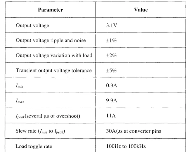
Conventional Power Distribution Architecture
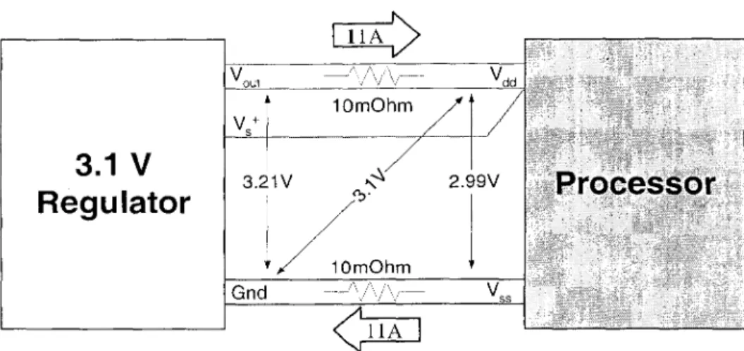
Effects of the Parasitic Resistance of the Supply Path on the
Instead, the inductance of the power supply determines how quickly power can be delivered to the load. In the previous discussion, the output of the silver box was modeled by an ideal voltage source to illustrate the effect of the power line inductance on the voltage on the processor pins.
Distributed Power Architecture
The VRM
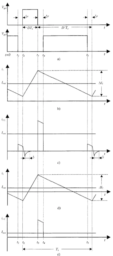
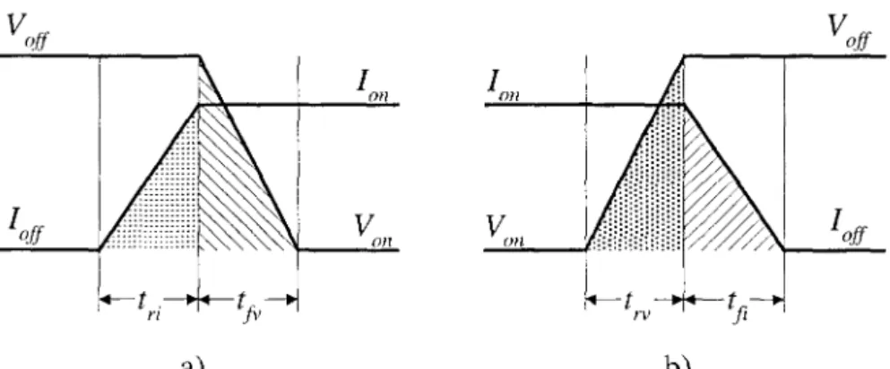
The total loss in the main switch of the regular buck topology can be expressed as: Thus, the loss in the main switch will not be affected by the reverse recovery of the body diode. A graph of the inductor current, phase junction and output voltage is given in Fig.
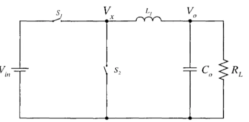
Overview of the Buck Converter Load Transient Response
Equation (3.19) gives an expression for 6 V5 as a function of switching frequency and output capacitance. To do this, the buck topology losses are analyzed in detail in Chapter 4 as a function of load current and switching frequency. Therefore, it is not possible to offset the output voltage according to the value of the inductor current.
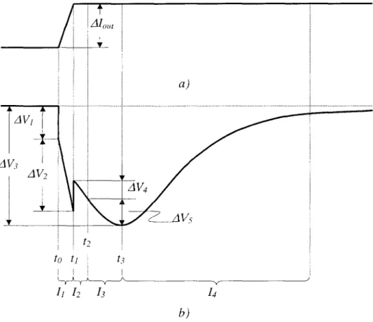
Interval 1 2
Interval 1 3
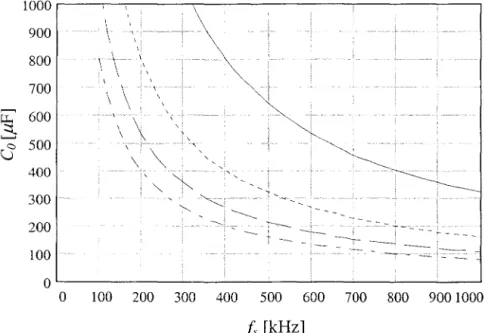
Thus, despite the second term in (3.14), it is possible to minimize ~V5 by increasing the output capacitance or reducing the size of the inductor. From (3.19), the amount of output capacitance required to achieve the prescribed maximum drop between () can be expressed as a function of the switching frequency with the inductor current ripple as a parameter.
Interval 1 4
Optimizing Voltage Budgeting
A plot of the output capacitance needed to achieve a combined voltage drop of 150 mV over the intervals lz and 13 is shown in Fig. Therefore, the size penalty resulting from the ESR and ESL of the selected capacitors is somewhat offset by the overall efficiency improvement.

Approaching the VRM Design Problem
- Merits of the High Switching Frequency
The obvious advantage of a higher switching frequency is the reduction of the physical size of the buck inductor. In short, a higher switching frequency allows the designer to reduce the size of both the buck inductor and the output capacitors and increase the bandwidth of the control loop.
VRM Design Philosophy
On the other hand, operation at a high switching frequency will reduce the efficiency of the converter and require advanced packaging techniques. The optimization of the transient response of the voltage-controlled step-down converter is carried out in Chapter 7.
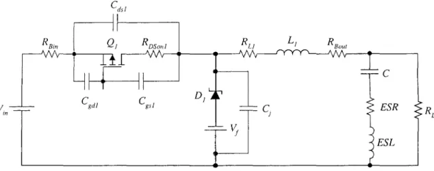
Overview of Various Loss Mechanisms in the Regular Buck Topology
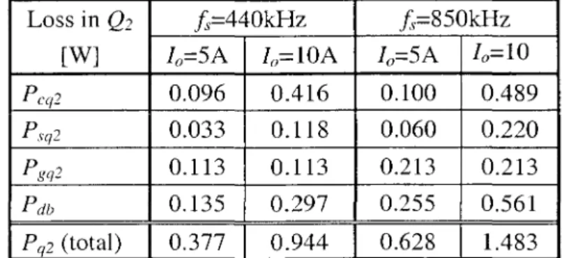
- Loss Mechanisms in the Schottky Diode
Conductivity loss in the main switch, Pel, can be expressed as:. where RDSoll1 is the drain to source on main switch resistor, Nml is the number of MOSFETs used in parallel, hrms is the rms current of the inductor and D is the duty cycle. The loss due to the junction capacitance can be expressed as: 4.11) where Cj is the capacitance of the Schottky diode junction.
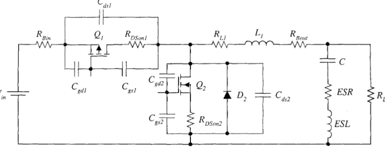
Overview of the Losses in the Synchronous Buck Topology
- Loss Mechanisms in the Main Switch
- Loss Mechanisms in a Synchronous Switch
The main loss mechanisms in Schottky are conduction loss, loss due to reverse bias leakage current and loss due to charge and discharge of junction capacitance. 4.17) where VGS2 is the drive voltage and QG2 is the total gate charge that must be supplied in order to enable the synchronous PET.
Efficiency Considerations
- Overview of Previously Published Work
- C Loss Distribution
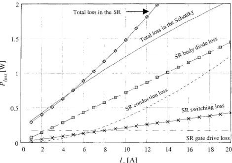
During tdl, the dominant loss component is reverse recovery of the body of the SR diode. However, the overall efficiency degradation due to SR body diode conduction is not independent of the inductor current ripple. A current sense resistor of 7mQ will reduce the efficiency of the module by 2-3% depending on the output voltage.
Experimental Verfification
On the Accuracy of the Component Level Distribution
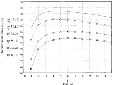
5.5-5.8 show that the overall circuit efficiency of both topologies was accurate, no experimental evidence has yet been presented to verify that the actual component level loss distribution can be trusted. Thus, since the accuracy of the overall circuit efficiency was not affected by the change in the operating point, Fig.
Conclusion
In the future, improved synchronous rectifiers could extend their competitiveness to higher frequencies and loads. As the switching frequency rises, the MOSFET's low on-resistance advantage (RDsoll) decreases due to increasing switching loss, gate drive loss, and diode body loss.
Overview of Previously Published Work
Since in some applications the VRM must operate at a relatively high input voltage (12V) and produce a relatively low output voltage (1.8V to 3.3V), the VRM synchronous converter deserves careful analysis and optimization. Therefore, a compromise must be found between size, load transient response and efficiency.
Overview of the Proposed Approach
Existing Controllers
In both cases, the loss in the body diode contributes significantly to the total loss. Results from Sections 6.5, 6.6 and 6.7 are combined in Section 6.S to show the full effect of the SR body diode conduction on the efficiency of a synchronous buck converter.
Overview of the Synchronous Rectifier Loss
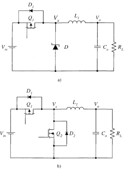
Although a synchronous buck converter always operates in the continuous conduction mode (CCM), since the waveforms in Fig. the SR body mode will produce losses during the two dead time intervals, tdl and td2.
Effect of tdl on the Synchronous Buck Efficiency in Mode 1
- Overall Efficiency Degradation Due to the Body Diode Conduction
- Overall Efficiency Degradation Due to the Body Diode Reverse
- Overall Efficiency Degradation Due to the Body Diode Conduction
On the other hand, during td2, the SR body diode carries the load current plus half of the inductor current ripple. The conduction loss of the SR body diode during both intervals depends on the size of the inductor current ripple.
Effect of tdl on the Synchronous Buck Efficiency in mode 2
Effect of td2 on the Synchronous Buck Efficiency
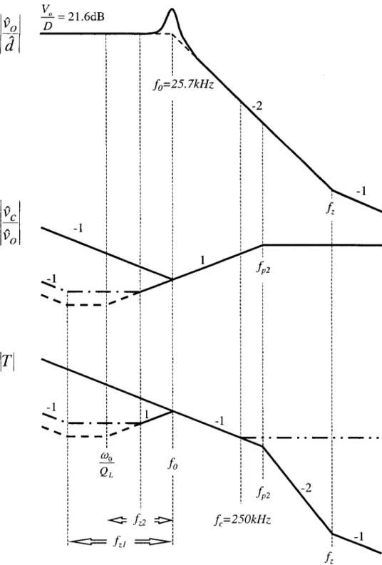
A typical open-loop output impedance of a synchronous buck converter is shown in Fig. 7.7a shown. o) is a zero due to the ESR of the output capacitors. The location of this pin determines the rate of output voltage recovery after a weld transition.

Effect of tdl and td2 on the Synchronous Buck Efficiency
New High Performance Gate Drive Circuit
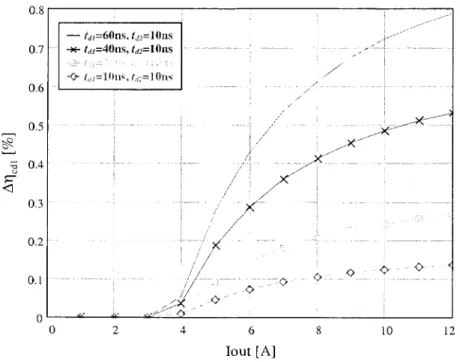
Therefore, with this circuit we have achieved independent dead time control to less than ions. The prototype achieves a minimum dead time of lOns and an adequate switching speed for lMHz operation.
Experimental Verification
Independent control of the delay before each switch turns on allows us to optimize each delay separately for maximum efficiency. When the dead time becomes too long (tdl=60ns), the advantage is offset by the soft switching of the conduction loss of the diode DI.
Conclusion
Namely, the loss due to body diode reverse recovery, dominant below tdl, will depend on the size of the ripple current. Therefore, the efficiency degradation due to SR body diode conduction decreases as the inductor current ripple increases.
Introduction
This article will focus on the design and optimization of the voltage mode control loop. An optimized control loop can save microfarads of output capacitance, thus reducing the size and cost of the point-of-load module.
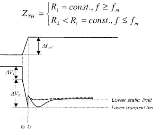
Buck Converter Load Transient Response Revisited
- Interval II
- Interval 1 2
- Interval 1 3
- Interval 1 4
Finally, the integral action of the control circuit eliminates any steady-state error in the output voltage and returns it to its nominal value, as shown in Fig. 7.3, by inspection it can be determined that Zo is the impedance of the output capacitors.

Conventional Loop Compensation
Closing the loop in this way ensures tight control of the output voltage due to high DC gain, and reasonably good transient response, depending on the bandwidth achieved. Consequently, the peak-to-peak voltage deviation due to a charge transient followed by a discharge transient is approximately equal to twice the peak output voltage deviation due to a charge transient.

Optimum Load Transient Response
If, on the other hand, the output voltage remained at or near the lowest level it had reached after the load switch, there would be additional headroom for the discharge switch; the peak-to-peak deviation of the output voltage can be roughly halved.
Achieving Optimum Transient Response With Voltage Mode Control
A typical open-loop output impedance of a buck converter, b) Target loop gain, c) Optimal closed-loop output impedance. Setting %1 above zero frequency results in a finite DC closed-loop output impedance, and thus, a finite output voltage drift (steady-state error).
Analysis and Simulation
Taking the inverse Laplace transform of (7.11) and (7.12) yields time domain equations for the converter output voltage, given by (7.13) and (7.14), respectively. The added value of (7.13) and (7.14) lies in the ability to investigate the contribution of each exponential term to the overall transient response and to derive closed formula expressions for peak voltage deviations.

Calculating the Peak Voltage Deviation
In other words, if lUe, lUzl, and W-.:2 are properly chosen, the transient response can be made to resemble the waveforms in Fig.
Experimental Verification
The transient response was measured for a load current step from 0.1 to 15A with a slew rate of 60All-ls and a frequency of 100Hz. The experimental results also confirmed the validity of (7.16): peak measured deviation under b was 56mV versus 60mV predicted by (7.16) and demonstrated in Fig.
Conclusion
Tight static voltage regulation and the desired shape of the converter's transient response were achieved by proper feedback loop design. Therefore, the overall efficiency of the module was improved by 2-3% by eliminating the current-sensing resistor without degrading the transient response.
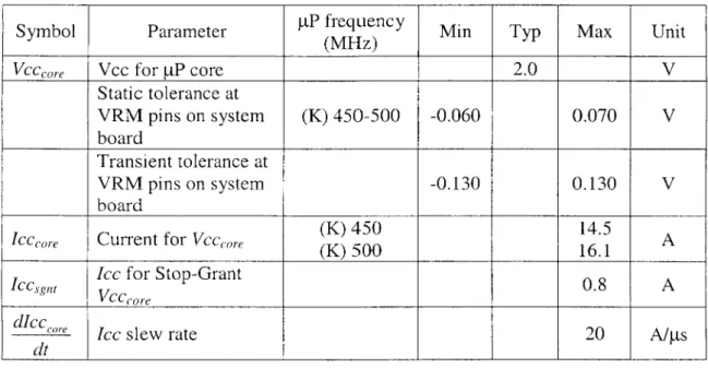
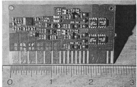
Board Specifications
Introductory Remarks
Furthermore, due to the height restrictions, the value of the inductor may need to be limited. As a result, a higher than usual switching frequency may have to be chosen to keep the inductor current ripple reasonable.
Power Stage Design
- Choosing the Inductor
- Switch Implementation
- A Choosing the Switches
- B
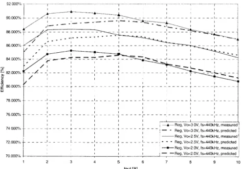
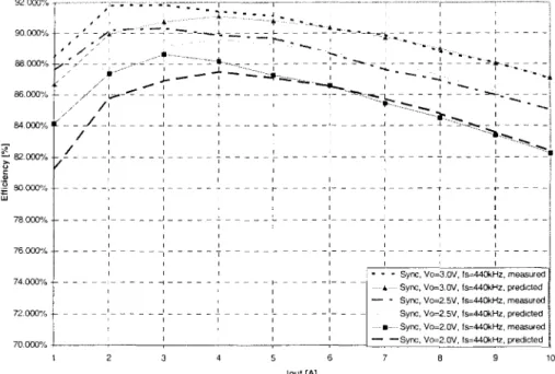
- Overall Circuit Efficiency
Similarly, using (3.19), we can plot the capacitance required to achieve ~V5=80mV as a function of the switching frequency. In contrast to the main switch (SJ), the synchronizing rectifier (SR) is switched on for approx. 70% of the switching period.

Control Loop Design
- Placing Compensation Poles and Zeros
- Circuit Implementation
- Circuit Simulation
- A Loopgain Calculation
- B Load Transient Response Simulation
This small improvement in efficiency does not warrant the increase in board size and cost. Due to the limitations described, the gain in compensation must be limited to one in fa.
Experimental Results
- Circuit Waveforms
- Loopgain Measurement
- Load Transient Response
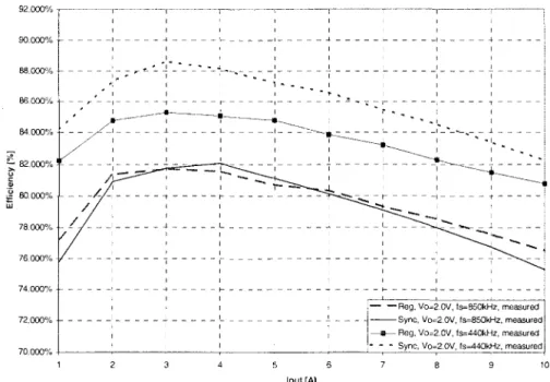
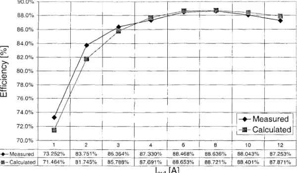
- Efficiency Measurements
- Physical Dimensions
The effectiveness of the module was measured with the board mounted on the evaluation board. From Table 8.3 we note that the length of the board is 1.2 times less than specified.
Concluding Remarks
A high switching frequency makes it possible to reduce both the physical size and value of the magnetic components. The only disadvantage of operating at a high switching frequency is the reduced efficiency of the power supply and more difficult thermal management.

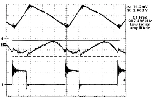
![Figure 6.3: Typical Si9140DB waveforms (top to bottom): phase node, V g], and V g2](https://thumb-ap.123doks.com/thumbv2/123dok/11010884.0/85.803.143.666.504.895/figure-typical-si9140db-waveforms-phase-node-v-v.webp)
