Introduction
Contributions
This capability enables self-calibration, self-correction and self-monitoring of the performance of integrated antennas in real time. The basic principles of operation and various methods of processing the PFRS readings are presented through a variety of examples.
Organization
The block diagram of the control circuits of the DPC phased array is shown in Figure 5.13. The maximum gain of the antenna (again from the output of the transistors to the far field radiation) in linear polarization mode. The simulated time domain waveforms of the QVCO quadrature outputs are also shown in Figure 5.40.
![Figure 2.1: Operation principle of Distributed Active Radiator (DAR) [5].](https://thumb-ap.123doks.com/thumbv2/123dok/10403307.0/34.918.284.638.111.337/figure-2-operation-principle-distributed-active-radiator-dar.webp)
Integrated Antennas: Motivations and Challenges
Integrated Antennas for Wireless Systems
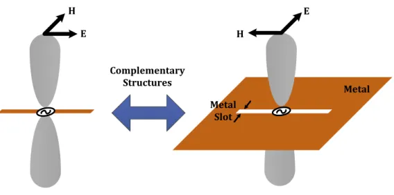
Surface Waves in Integrated Antennas Substrate
The presence of the substrate plays an important role in the design and performance of integrated antennas. As an example, Figure 2.5 shows the different substrate modes that are excited for a dipole antenna as well as a slot antenna implemented on quartz and GaAs substrates as a function of the ratio of substrate thickness (h) to wavelength (λ0).
![Figure 2.5: Normalized power versus substrate thickness for (a) dipole on quartz substrate, (b) dipole on silicon or GaAs substrate, (c) slot on quartz substrate, and (d) slot on silicon or GaAs substrate [22].](https://thumb-ap.123doks.com/thumbv2/123dok/10403307.0/37.918.219.695.100.789/figure-normalized-substrate-thickness-substrate-substrate-substrate-substrate.webp)
Effects of Process and Environmental Variations
It can be seen that this variation is smaller and therefore easier to manage at larger process technology nodes compared to the advanced smaller nodes.
![Figure 2.8: Average number dopant atoms as a function of technology node [33].](https://thumb-ap.123doks.com/thumbv2/123dok/10403307.0/40.918.308.613.223.439/figure-average-number-dopant-atoms-function-technology-node.webp)
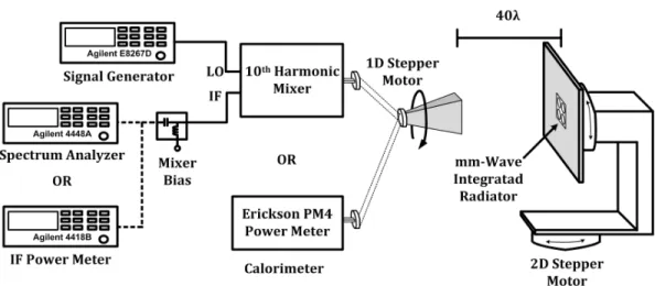
Indirect Measurement of Far-Field Radiation Properties
The efficiency from transistor output (including impedance transformation, signal routing and antenna) to far field radiation is 12%.
Proximal-Field Radiation Sensors
Introduction
Integrated Antennas on Dielectric Substrates
Proximal-Field Sensing
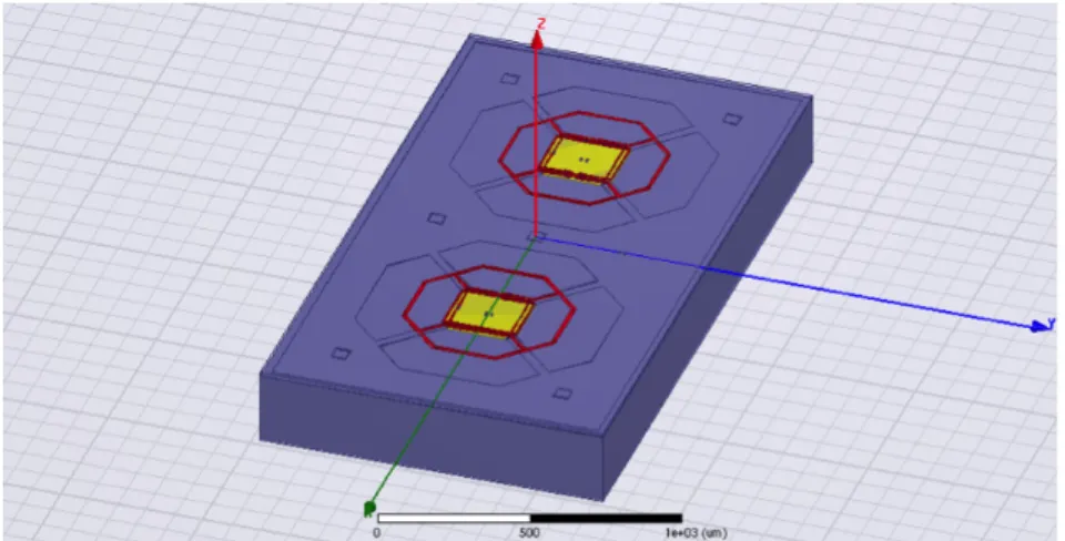
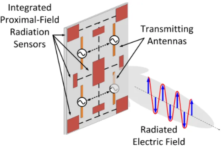
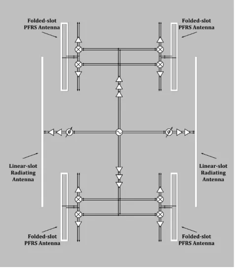
Proximal-field radiation sensors (PFRS) are a number of small sensing antennas that are strategically placed and integrated on the same substrate as the transmitting antennas (Figure 3.6) and measure certain properties of the electromagnetic field in the immediate vicinity of the radiating antennas [49 ]. Shown in Figure 3.10 are two of such undesirable mechanisms that can have a destructive impact on the PFRS antennas on this chip: 1) coupling to strongly driven points through the drive circuit (points A, B and C) to the sensors through substrate, and 2) incident electromagnetic waves on the integrated radiator from external sources.
PFRS Data Capture Fundamentals
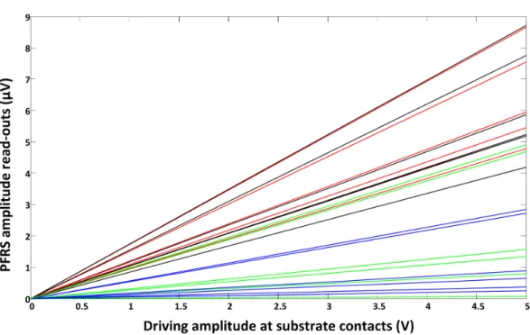
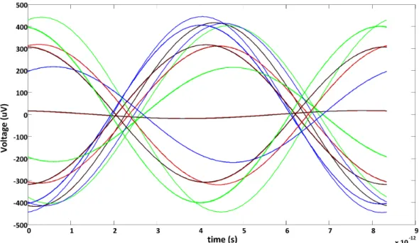
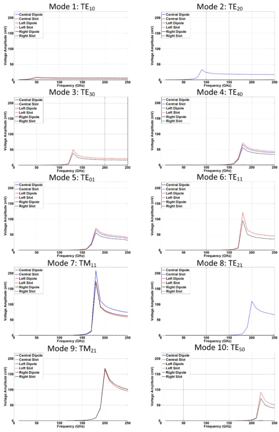
Again, the magnitude of the voltages picked up by each sensor versus the frequency of excitation for different modes is plotted on the same scale to simplify comparison and is shown in Figure 3.21. The magnitude of the voltages picked up by the TE/TM sensors versus the excitation frequency is plotted in Figure 3.26 using the same scale for all modes.
PFRS Data Processing
- Symmetry-based Methods
- Statistical Methods
- Simulation-based Methods
The locations of the plots correspond to the locations of the sensors on the chip. This symmetrical behavior of the signals due to the symmetrically placed gates is another tool that can be used to observe the degradation of the chip's performance. Due to the circular symmetry of the radiation structure, the 36 outputs of the PFRS antennas can be divided into nine sets.
Shown in Figure 3.39, we can see such a combined metric and its relationship to the strength of the radiated signal in the broadside direction based on the received signals of a receiving antenna placed in the same direction on top of the integrated radiator. The resulting linear polarization of the radiated field for the two cases of ∆ψ =0◦and∆ψ = 180◦ is shown in Figure 3.41. However, the polarization of the radiated electric field is solely determined by ∆ψ in a similar way.
Shown in Figure 3.43 are the same PFRS outputs for such a scenario when a phase difference is applied between the phase references of the transmit antennas on the left with respect to the transmit antennas on the right. The polarized nature of this antenna enables performance evaluation for different polarization angles of the radiated electric field.
PFRS Implementation on a PCB prototype
- Prototype Design
- Data Interpretation
- Measurements
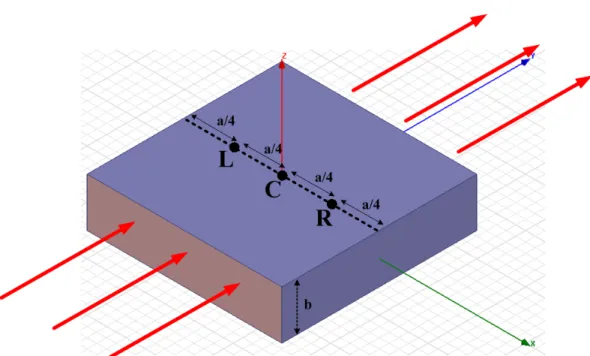
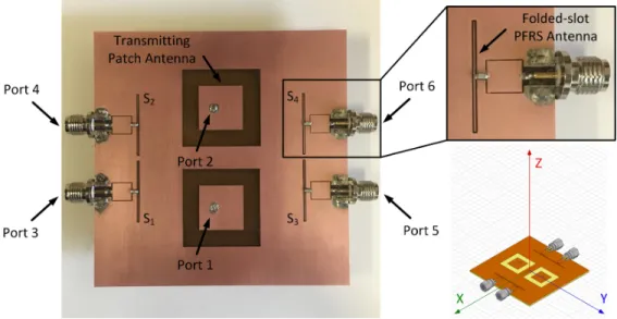
This allows direct control of the drive of the transmitter antennas and accurate reading of the sensor antennas. The first parameter that we can investigate in this design is the direction angle of the radiated far-field beam in the yz plane as a result of the phase difference between the inputs of the patch antennas. A simple way to derive this phase difference is to monitor and compare the amplitudes of each of the pairs of sensors S1, S2orS3, S4 that are placed symmetrically with respect to the x-axis (Figure 3.55).
We can also extract the mathematical relationship between the readings of PFRS antennas and various components of the radiated fields of the transmitting antennas (and thus the polarization of the radiated electric field) in each direction using the method described in section 3.5.3.1. Therefore, the distortions of the predicted radiation properties by PFRS antennas, caused by interfering objects in the radiation path and the direct proximity of the radiating antennas, are minimal. The HFSS simulation setup shown in Figure 3.57(a) examines an example of such a scenario for our prototype, where a metal reflector λ/2× λ/2(= 3 cm× 3 cm) is placed in the radiation path of the transmitting beam . patch antennas at the vertical distance h from the printed circuit board.
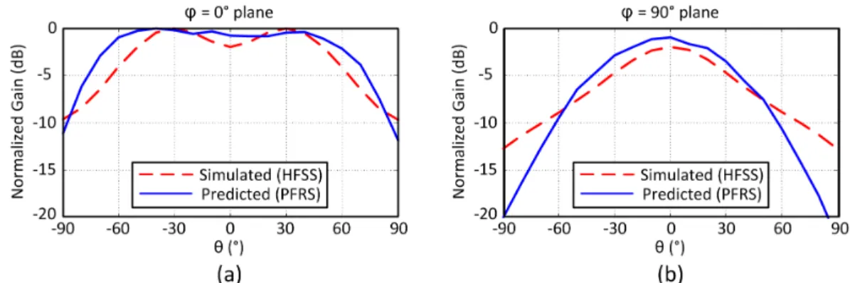
This is further illustrated in Figure 3.62, where the relative phases of the two patch antennas are switched by 180◦ respectively to significantly change the radiation pattern in the φ = 90◦ plane, yet for all three cases the simulated, measured, and sensor-predicted normalized gain patterns they match very precisely. As mentioned earlier, PFRS readings can also be used to predict more specific properties of far-field radiation, such as the polarization of the radiated electric field.
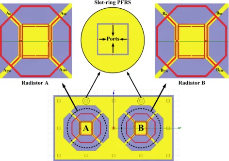
PFRS Implementation on an IC prototype
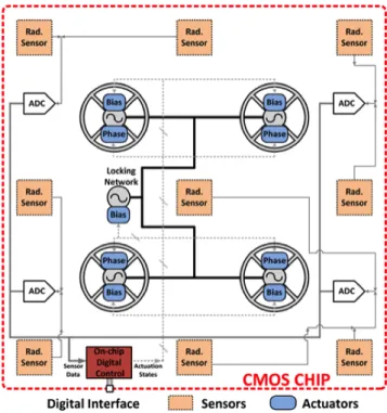
- System Architecture
- Radiator Design
- PFRS Design
- Measurements
72 The simulated and measured relationship between the amplitudes of the signals received by the S1 and S2 PFRS antennas and the phase difference between the transmitting patch antennas as a measure to track the beam direction angle is shown in Figure 3.64. Two of the oscillators provide the quadrature signals that allow 360◦ phase control of the drive signals with appropriately weighted summation of the I and Q components through the phase rotators. The schematics for the buffers and the phase shifter are shown in Figure 3.70 and Figure 3.71, respectively.
The simulated strengths of the signals picked up by each PFRS antenna for the same phase rotator settings as the previous section are plotted in Figure 3.74. A conceptual block diagram of the masking scheme used for coherent PFRS signal detection is given in Figure 3.75. The buffer stages in the LO distribution network are the same cascode buffer stages used in the drive circuits of the transmitting antennas.
The same phase rotator control voltages used to achieve 0◦ to 360◦ phase control between the two broadcast antenna drivers in simulation (Figure 3.72) are applied to the drive circuit to measure detection circuit outputs. Calibrated measured down-converted PFRS readings for both I and Q components of all sensors versus the phaserotator settings are shown in Figure 3.79.
Conclusions
The total simulated output power going into the four antenna ports is 3.6 dBm. The polarization of the far-field electric field can be defined by the ratio of the polarization axis and the polarization angle. The supply lines from the locking network are routed above the ground plate near the antennas.
The simulated gain patterns of the array for both linear and circular polarization modes are shown in Figure 5.33. Antenna drive circuit: Figure 5.34 shows the details of the drive circuit for each antenna element.
Multi-Port Driven Antennas
Introduction
Multi-Port vs. Single-Port Antennas
- Limitations of Single-Port Antennas
- Advantages of Multi-Port Antennas
However, as integrated circuit (IC) technologies have advanced to enable the integration of antenna and circuit blocks on the same substrate at mm-wave frequencies, the key factors that determine overall system cost have also changed. At high mm-wave frequencies, the size of the antenna is small enough to justify the cost of integrating it on the same substrate as it. This is mainly because the radiation resistance, and thus the input impedance of the single-port antenna must be high so that it is much greater than the loss resistance.
The use of an MPD antenna in an integrated transmitter allows hybrid design of the antenna and the drive circuits also implemented on the same substrate. This in turn takes advantage of the additional design space provided by the co-design. Due to the elimination of these blocks, the driver circuit can now be placed very close to the drive ports of the antenna.
In an MPD antenna, the location of the drive ports can be chosen such that virtual short circuits are created on the antenna. For high power applications, the breakdown voltage of the output transistors limits the peak voltage at the drive points.
![Figure 4.2: Multi-port driven radiator design methodology for integrated radiation where drivers directly feed multiple ports of the antenna [6]](https://thumb-ap.123doks.com/thumbv2/123dok/10403307.0/117.918.283.633.449.696/figure-radiator-methodology-integrated-radiation-drivers-directly-multiple.webp)
Integrated Multi-Port Driven Slot Ring Traveling-Wave Radiator
- A 2 × 1 Integrated DPC Radiator Array
- A 2 × 2 Integrated DPC Radiator Array
- A 2 × 2 Integrated Slot-Based DPC Radiator Array
Two plane models of the measured height are shown in Figure 5.23 for φ= 0◦, along the string axis, and φ = 90◦, perpendicular to the string.
Polarization Modulation
- Prototype: Transmitter and Receiver Architectures for Pol-M 170
It also provides a bias path from the outer ground plane to the inner ground plane through the "signal line" of the CPW transmission line since there is now a solid piece of metal connecting the two ground planes. Here, the polarization symbols are the different polarization angles of the transmitted EM waves over each symbol period, Tsym. Since Pol-M is a spatial concept, it is completely independent and orthogonal to existing phase and amplitude modulation of the signal's time domain waveform.
In this block diagram, "Signal Modulator" refers to the entire set of blocks, which only modulate the amplitude and phase of the signal. Depending on the application, all or different sets of baseband inputs modulate the amplitude and phase of the signal and the polarization of the transmitted EM waves, thus resulting in simultaneous phase, amplitude and polarization modulation. The baseband inputs controlling the two 360◦phase rotators perform two simultaneous tasks: 1) setting the relative phases of the antenna drive gates with respect to each other (modulating.
A possible implementation of a transmitter capable of performing Pol-M. 170 polarization [103]) and 2) setting the relative phases of the antenna's driving gates with respect to the QVCO phase (modulating signal phase). In addition, other baseband inputs, which drive variable gain amplifiers, modulate the amplitude of the signal, resulting in simultaneous modulation of the phase, amplitude, and polarization of the transmitted EM waves.
Conclusions
Conclusions
![Figure 2.2: Block diagram of the Multi-Port Driven (MPD) antenna [6].](https://thumb-ap.123doks.com/thumbv2/123dok/10403307.0/34.918.281.636.407.762/figure-block-diagram-multi-port-driven-mpd-antenna.webp)