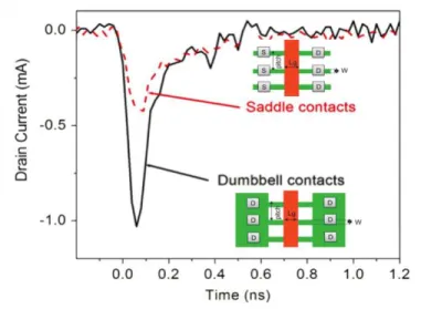
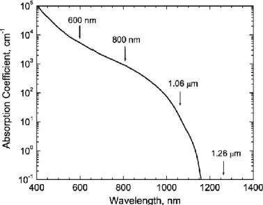
Room temperature absorption spectrum of silicon in the visible and near infrared region of the. Moreover, the reduced hole lifetime in the GaAs buffer layer also contributes to the relative reduction of the bipolar gain in these devices.
MOSFET scaling
Metal-gate/high-k gate stacks were introduced in the 45 nm node to reduce gate leakage and eliminate polysilicon depletion [23], [24]. The devices exhibit excellent short-channel characteristics (SS = 65 mV/dec, DIBL = 42 mV/V) at performance levels comparable to finFET reference devices [28].
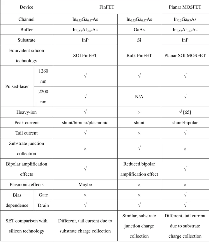
III-V MOSFETs
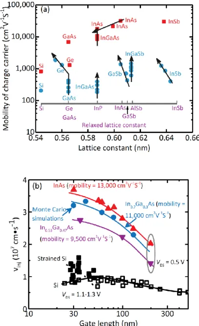
The low-field carrier mobility and electron injection rate in III-V compound semiconductors are shown in Fig. Similar to silicon technology, InGaAs FinFETs [8]–[11] and InGaAs gate-all-around nanowire transistors [12]–[14 ] have been developed to reduce short-channel effects.
Radiation environments
Cosmic rays, including the galactic cosmic rays, and the solar cosmic rays include protons and heavy ions. When cosmic rays penetrate the top of the Earth's atmosphere, they interact with nitrogen and oxygen atoms and produce a "burst" of secondary particles, including protons, electrons, neutrons, heavy ions, muons and pions [2], among which neutrons is the most important product.
![Fig. 2.5. The charged particles trapped by the Earth’s magnetosphere [38].](https://thumb-ap.123doks.com/thumbv2/123dok/10740121.0/20.918.269.649.331.635/fig-2-charged-particles-trapped-earth-magnetosphere-38.webp)
Single-Event Effects
- Charge deposition
- Charge collection mechanism
- Shunt effect
- Single-event transient in silicon MOSFETs
- Bipolar amplification effect
- Plasmonic effect
The most sensitive regions are reverse-biased p-n junctions due to the high electric field presented in the depletion region. As the active channel volume decreases, the charge collection in the drain region masks the contributions of the fins [52], [53].
Introduction
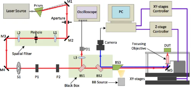
Device structure and experimental setup
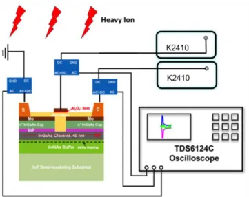
Devices with different fin widths were tested with both pulsed laser and heavy ion irradiation. Transients are captured using a Teledyne Lecroy LabMaster 10-36Zi-A oscilloscope with a front-end bandwidth of 36 GHz and a sampling rate of 80 GS/s for pulsed laser experiments and a Tektronix TDS6124C oscilloscope with a front-end bandwidth of 12 GHz and 20 GS/s sampling rate for heavy ion experiments.
Experimental results and discussion
Pulsed-laser induced charge generation
Maximum drain current (a) and drain accumulated charge (b) along a line scan for InGaAs FinFETs with different fin widths during TPA testing. Drain current transients for InGaAs FinFETs of different fin widths under TPA test (peak drain current taken as absolute value). The maximum drain current along a line scan at different drain biases is shown in fig.
The peak drain current is much lower when the source and drain are tied together.
Heavy-ion induced charge generation
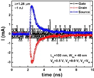
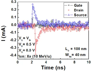
There is asymmetry in the drain and source transient signals, with the peak drain current showing a delay compared to the peak source current. Collected charge and peak drain current during Xe irradiation for devices with different fin width (a) and drain bias (b). Devices with narrow fins exhibit smaller cross-sections compared to devices with wider fins. a) Collected charge, peak drain current and (b) SET cross section for a 40 nm device with heavy ion irradiation at different LET in In0.53Ga0.47As.
The SET cross section increases as LET increases, and no saturation cross section is observed.
TCAD Simulations
Geometric effect
Channel modulation by the substrate
When the charge density under the rib increases from 2 × 10¹⁹/cm3 to 2 × 10²¹/cm3, the electron density in the channel is greatly affected. In devices with wider fins, the charge acts as a feedback gate that modulates the charge density in the channel. Devices with narrower fins are less affected by the modulation effect of the rear gate due to the shorter length of the rear gate, which is equivalent to the width of the fin, and the channels are more strongly modulated with two side gates.
Electron density distribution (b,c,d) for 20 nm fin width devices with different doping in the red region (a).
Optical Simulations
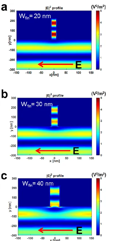
This model system evaluates the optical response of a fin to sub-band-gap irradiation, as is the case for the majority of the fin (180 nm out of 220 nm) in the tested device. In this first-order approximation, the integrated E2 intensity in the fins is assumed to be proportional to the energy absorbed in the fins, which in turn is related to the charge generation in the fins. The change in the distance between the E2 intensity oscillations for the different fin widths can be explained by traditional optical interference effects between the incident and reflected light waves [95].
The higher peak E2 intensity in the narrower fins shown by examination of the color bar scale in Fig.
Conclusion
Therefore, the integrated E2 intensity at the 40 nm fin is larger than that at the 30 nm fin, which in turn is larger than that at the 20 nm fin in both optical simulations and laser test experiments. Additionally, multiple reflections are likely to lead to a significant increase in the local e-h pair density in smaller devices, leading to an improved recombination rate. Based on these general considerations, we believe that optical phenomena will play an important role in laser-based testing of FinFET technology at the 14nm node and below.
These include emerging FinFETs and Gate-all-around (GAA) devices, so this is an important factor in testing nanometer devices.
Introduction
3-D TCAD simulation shows that the transient peaks are mainly due to charge deposition from the channel. Optical simulation shows that increased charge deposition in the fin channel can be due to plasmonic effects.
Device structure and experimental setup
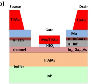
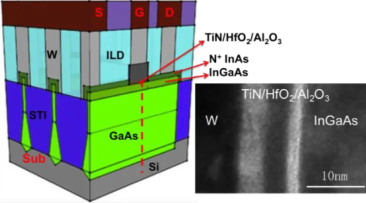
Area mapping illustrates the enhanced SET sensitivities of plasmonic effects in the fin region. a) Schematic cross-section and (b) side view of an InGaAs planar MOSFET (not drawn to scale). 40 nm SiO2 acts as a hard mask, which electrostatically decouples the top gate from the channel. InGaAs planar MOSFETs also have a 0.4 μm In0.52Al0.48As buffer layer grown on a 600 μm semi-insulating InP substrate.
The DUTs are irradiated from the back by focusing a pulsed laser spot close to the channel region.
Experimental results and discussion
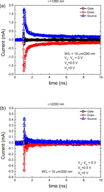
The peak discharge current along a line scan for an InGaAs FinFET at different drain biases is shown in Fig. Peak discharge current along a line scan at different drain biases for an InGaAs FinFET with wavelengths at (a) 1260 nm and (b) 2200 nm. Peak drain current along a line scan at different drain biases for a planar InGaAs MOSFET with wavelengths at (a) 1260 nm and (b) 2200 nm.
The black box in each figure marks the sensitive region in the xy plane at each wavelength.
Plasmonic effect in InGaAs FinFETs
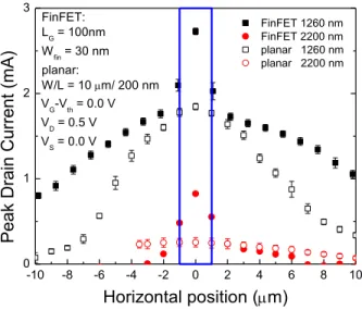
Comparison of the peak drain current along a line scan between an InGaAs FinFET (solid symbols) and a planar InGaAs MOSFET (open symbols) with a wavelength of 1260 nm (black) and 2200 nm (red). Comparison of the peak drain current along a line scan between an InGaAs FinFET with a fin height of 220 nm (black box) and 40 nm (red circle) [56] at a wavelength of 1260 nm. This suggests that plasmonic effects may contribute to the charge deposition in the InGaAs FinFET, while this is not the case in the planar InGaAs MOSFET.
Similar to the InGaAs planar MOSFET, no steep rise is observed in the 40 nm fin height device.
TCAD simulation
When the laser spot hits the fin from -1 μm to 1 μm, the peak current suddenly increases in the FinFET at both wavelengths. From the 22 nm technology node to the 10 nm technology node, the filament height increases while the fin width decreases [78], which may result in increased plasmonic effects in newer technologies. currents for these two methods of charge generation are the same, suggesting that the peak transient is primarily due to channel charge generation. The sudden increase in peak current in the fin region may be due to plasmonic effects in the fin channel. a) Load injection scheme in SET simulations.
For charge generation in both the channel and the substrate, the electron flow from the substrate is observed, while no electron current flows when charge is generated in the channel only.
Conclusion
Electron current density for charge deposition in both channel and substrate (left) and channel only (right) (a) 50 ps after charge deposition and (b) 500 ps after charge deposition. TCAD simulation shows that the transient peaks are mainly due to charge generation in the channel. Optical simulation shows that increased charge generation in the fin channel can be due to plasmonic effects.
Plasmonic effects can play an important role for pulsed laser SET characterization of modern CMOS technologies.
Introduction
Experimental details
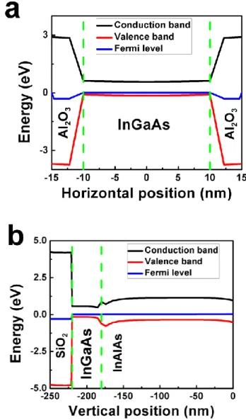
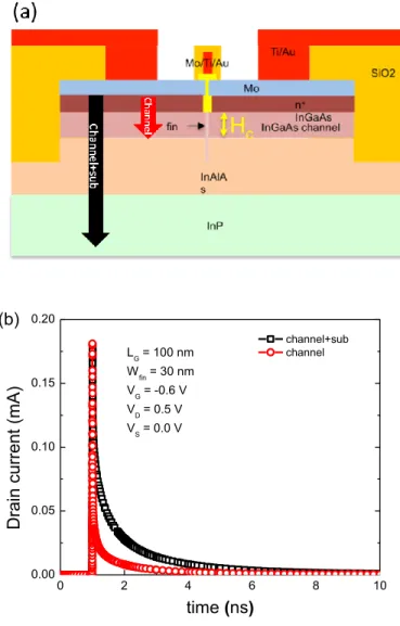
Energy band diagram for a Si-based InGaAs FinFET for a dashed line (dashed red line in Fig. 5.1) through gate to substrate.
Experimental results and discussion
However, the generated holes in the silicon-substrate devices are efficiently collected by the substrate contact, contributing to the substrate charge collection. For these bias conditions, drain (or source) and substrate junction charge collection are dominant since there is no source-drain electric field. This suggests that junction charge collection contributes significantly to these bias conditions, similar to what is observed for silicon and SiGe FinFETs and different from other InGaAs FinFETs on semi-insulating substrates [54], [55].
Peak drain current along a line scan at different drain biases for an InGaAs FinFET on silicon (a) and an InGaAs FinFET on InP (b) [55].
![Fig. 5.5. Normalized (to fin number) drain currents between an InGaAs FinFET on silicon (black) and previous results for an InGaAs FinFET on InP (red) [55]](https://thumb-ap.123doks.com/thumbv2/123dok/10740121.0/75.918.273.644.674.946/normalized-currents-ingaas-finfet-silicon-previous-results-ingaas.webp)
TCAD simulations
Parasitic bipolar amplification
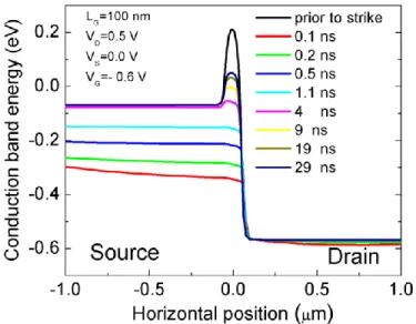
Holes accumulated in the channel or under the channel will produce parasitic effects of bipolar amplification. Evolution of along-channel conduction band energy after charge deposition for InGaAs FinFETs on silicon substrate. Continuous electrostatic potential contours for an InGaAs FinFET before laser shock (left) and 100 ps after shock.
Prior to charge deposition, there is a 0.3 eV barrier to electrons flowing from source to drain.
Hole collection by the substrate
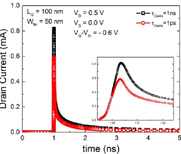
Reduced carrier lifetime in GaAs
Black squares show transients with a carrier lifetime of 1 ns, and red circles show transients with a carrier lifetime of 1 ps. The red curve has a lower and narrower transition peak compared to the black curve due to the reduced carrier lifetime in the GaAs layer. The figure on the left shows the hole density distribution for a GaAs layer with a carrier lifetime of 1 ns.
The figure on the right shows that the hole density below the channel decreases due to the reduced carrier lifetime (1 ps).
Conclusions
Thean, “InGaAs gate all-round nanowire devices on 300mm Si substrates,” IEEE Electron Device Lett., vol. Lotshaw, “The contribution of nuclear reactions to a single heavy ion event perturbed cross-sectional measurements in a high-density SEU-hardened SRAM,” IEEE Trans. Pease, “Subbandgap laser-induced effects from single events: carrier generation via two-photon absorption,” IEEE Trans.
Boos, “Gate bias dependence of single-event charge collection in AlSb/InAs HEMTs,” IEEE Trans. Weller, “The impact of depletion region potential modulation on ion-induced current transient response,” IEEE Trans. Campbell, “Critical evaluation of the pulsed laser method for single-event effects testing and fundamental studies,” IEEE Trans.
Charge generation mechanism for 1260 nm laser
Ions that comprise the LBNL 10 MeV/u cocktail
Charge generation mechanism in InGaAs FinFETs and planar MOSFETs
Charge generation mechanism for 1260 nm laser
Summary of single-event transients on sub-10 nm node III-V MOSFETs is this dissertation
![Fig. 2.6. Relative abundance of the elements from hydrogen to the iron group [39].](https://thumb-ap.123doks.com/thumbv2/123dok/10740121.0/20.918.270.644.733.998/fig-relative-abundance-elements-hydrogen-iron-group-39.webp)
![Fig. 2.8. Charge generation and collection phases in a reverse-biased junction and the resultant current pulse caused by the passage of a high-energy ion [47]](https://thumb-ap.123doks.com/thumbv2/123dok/10740121.0/24.918.208.714.110.770/charge-generation-collection-reverse-junction-resultant-current-passage.webp)
![Fig. 2.9. Illustration of ion track shunt effect in two-junction experimental structure [49]](https://thumb-ap.123doks.com/thumbv2/123dok/10740121.0/25.918.287.629.262.543/fig-illustration-track-shunt-effect-junction-experimental-structure.webp)
![Fig. 2.10. Transient drain currents induced by pulsed laser irradiation in 0.25 μm NMOS and 50 nm NMOS transistors [58]](https://thumb-ap.123doks.com/thumbv2/123dok/10740121.0/26.918.149.784.128.375/transient-drain-currents-induced-pulsed-laser-irradiation-transistors.webp)