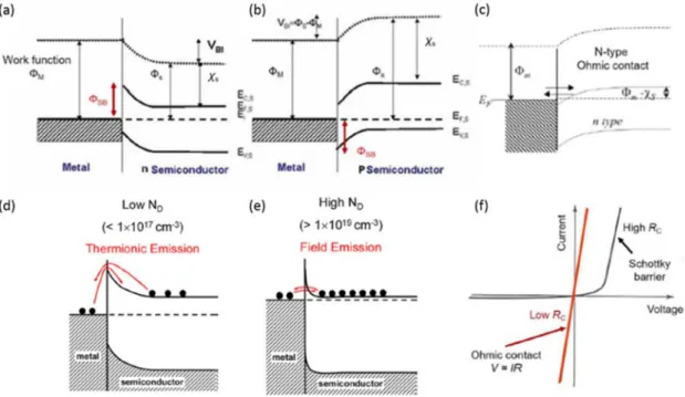
In particular, the realization of practical devices based on 2D materials will require overcoming the typical Fermi-level pinning limitations of electrical contacts at the metal-semiconductor interface and finally approaching the ideal Schottky-Mott limit. The Schottky barrier heights of WS1.94Te0.06-FETs with WTe2/Au contacts also follow the general trend of the Schottky-Mott boundary, implying high-quality electrical contacts.
Electronic structures of monolayer graphene
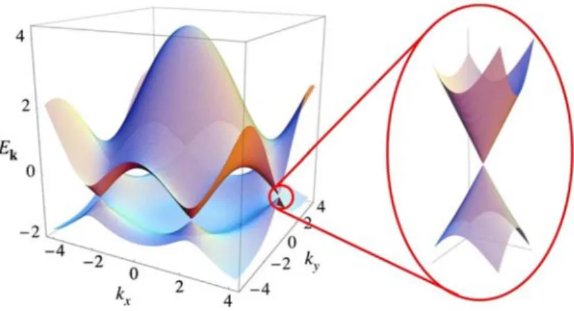
In the reciprocal lattice, there are two degenerate and nonequivalent points K and K located at the corners of the first Brillouin zone (BZ). In the above equation, is the envelope function (or called the spin wave function), which can be converted back to the wave function in real space.
Nanophotonics: light-,atter interaction in TMDCs materials
- The growth of single crystalline bilayer graphene
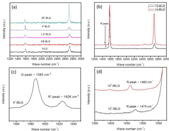
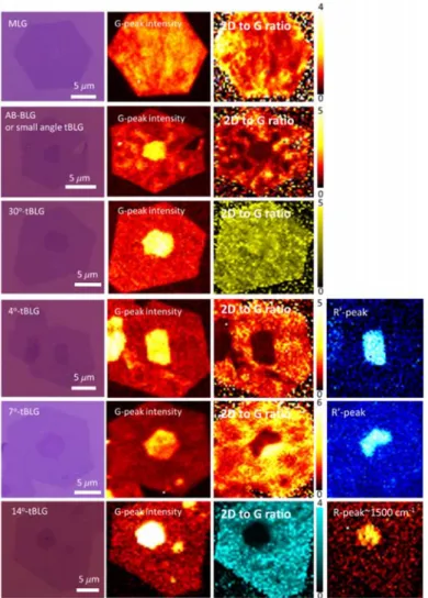
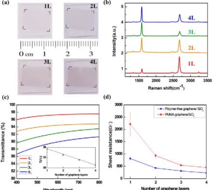
- Raman spectroscopic characterizations of monolayer, bilayer, and twisted bilayer graphene graphene
- Raman spectroscopic analysis of twisted bilayer graphene (tBLG)
- Work function analysis on tBLG
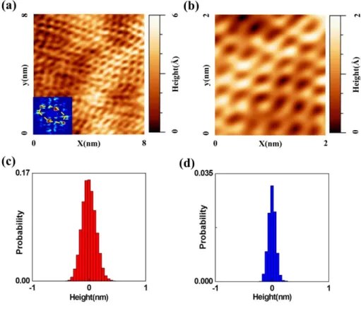
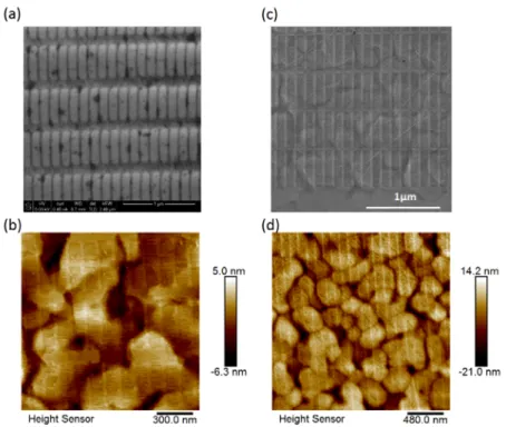
- Atomic structure of the polymer-free transferred monolayer graphene
- E-Beam Lithography
- Helium/Neon focused ion beam lithography
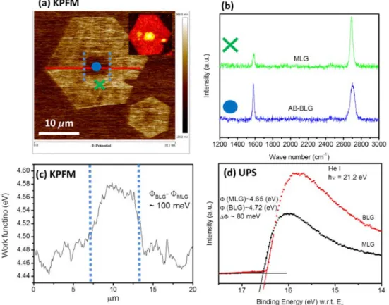
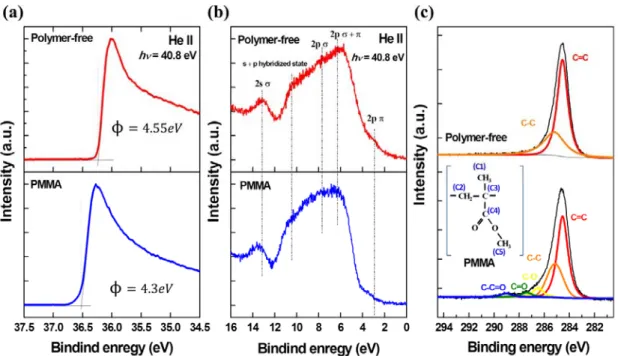
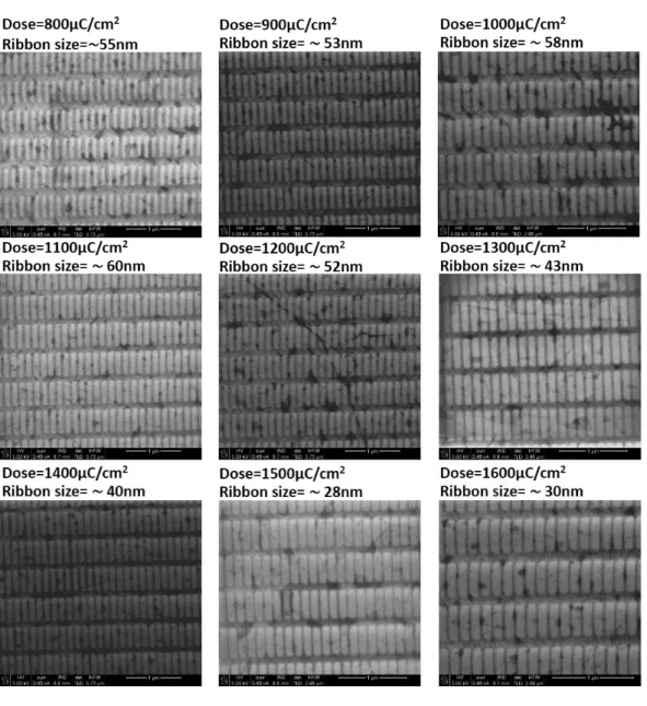
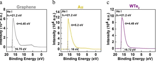
The work function of the He II UPS valence band spectra of the polymer-free transferred graphene sample and the PMMA-transferred graphene sample. Comparison of the edge roughness of GNRs patterned by e-beam lithography (left panels) and by helium/neon focused ion beam lithography (right panels).
Graphene device technologies
- Electrical mobility measurements on monolayer graphene-based field effect transistors
- Electrical FET devices analysis on tBLG
- Graphene-based vertical tunneling devices
- Applications in graphene-based organic solar cell
2.18 (a), where the two black lines indicate the BLG channel with the above dimensions, and the inset shows schematic representations of the cross-section of the device. Graphene (Gr)-boron nitride (h-BN) heterostructure in our silicon-based tunneling device. a) The side view of the tunnel structure structure. Here our tunneling device is the size of a micrometer, and n++-Si is used as one of the electrodes.
Atomic-scale structural and chemical characterization of hexagonal boron nitride layers synthesized at the wafer-scale with monolayer thickness control synthesized at the wafer-scale with monolayer thickness control
The crystal structures and chemical compositions of the resulting h-BN films are also characterized by atomic force microscopy (AFM), Raman spectroscopy, infrared transmission measurements, and x-ray photoelectron spectroscopy (XPS). The electrical properties of h-BN thin and thick films were systematically measured in metal-insulator-metal (MIM) tunnel devices to understand the dielectric properties of these films. Our results demonstrate a new and state-of-the-art standard for the synthesis of large-area h-BN films, potentially enabling applications in nanoelectronic and nanophotonic devices.
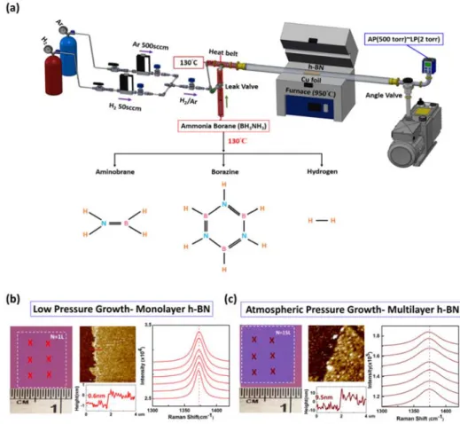
CVD synthesis of mono- and multilayer h-BN with atomically thickness control
To atomically control the thickness of the h-BN layer, it is very important to have a flow valve to control the flow rate of the precursor. Therefore, we can systematically vary the thickness of the grown h-BN films by using a flow valve to control the borazine flow rate (or borazine partial pressure). In Figure 3.4 below, we show the quantitative dependence of the h-BN film thickness on the partial pressure of the precursor (borazine).
Atomic structures of monolayer h-BN and multilayer h-BN
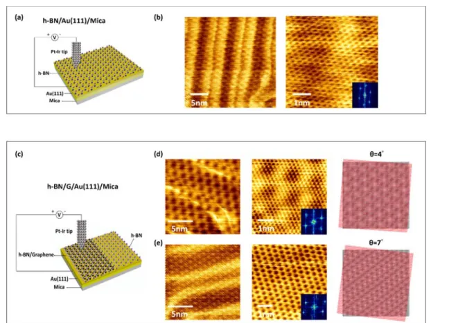
The twist angle between the h-BN and graphene lattice can be deduced from the structure of the Moiré pattern and is given by. Alternatively, the twist angle can also be extracted by performing a fast Fourier transform (FFT) analysis of the STM images, as shown in the inset of Figure 3.5 (d) and (e). The atomic resolution STM images presented here can be achieved at imaging locations over a large area of the wafer-scale sample, indicating excellent h-BN sheet surface quality for layers transferred with the polymer-free transfer method and the existence of supports a high crystalline quality in CVD-grown h-BN down to the monolayer level.
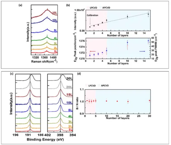
Raman spectroscopic analysis of h-BN
The full width at half maximum vs. number of h-BN layers showing a constant increase of FWHM with the h-BN thickness. Furthermore, it can also be seen that the intensities of B1s and N1s increase with the increasing layer thickness of our film. Finally, quantitative analysis of the B1s and N1s spectra shows that the B/N atomic ratio in our film was 1 ± 0.6% across the thickness range.
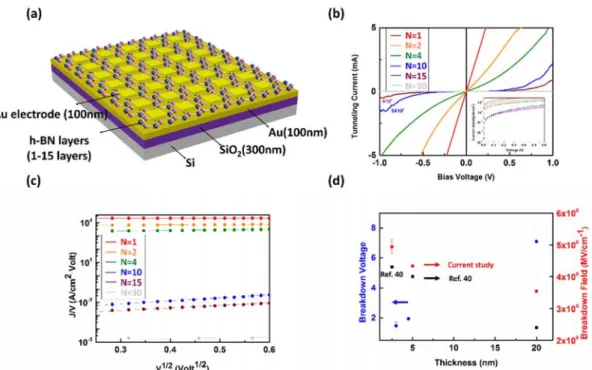
Electrical measurement on metal/h-BN/metal (MIM) capacitors
The h-BN thickness range was less than 5 nm. d) Degradation characteristics as a function of h-BN film thickness. The improved ability of the Ni-Cu alloy to degrade polyaminoborane residues improves the surface cleanliness of the alloy during h-BN growth. Thus, by controlling different pathways of the chemical reaction, we demonstrated further control of the ZPL energy distribution.
Summary of synthesis and properties of 2D insulator (h-BN)
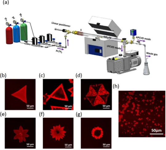
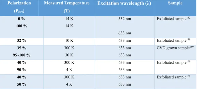
Monolayer transition metal dichalcogenides (TMDCs) in the 2H phase are semiconductors that hold promise for opto-valleytronic and opto-spintronic applications due to their strong spin-valley coupling. Similar symmetries are also found in the Raman spectral intensity assignment for (e) the A1g mode and (f) the E2g1 mode. Here we report the successful CVD growth (Figure 4.2) of monolayer h-WS2 that shows significant circular polarization already at room temperature and almost 90% circular polarization (CP) in the environment.
CVD synthesis of monolayer h-WS2 with special emission pattern
The formation of nuclei is strongly influenced by the mass flow of the metal precursor and the size of growth domains is dominated by the growth rate. In contrast, a low mass flux of the metal precursor favors the formation of single crystals with small domains when combined with a low growth rate, and a large single-layer single crystal when combined with a high growth rate. By controlling the different partial pressures of hydrogen gas, we can control the shape of the single crystalline WS2, from triangular, truncated triangular, hexagonal to dodecagonal shapes.
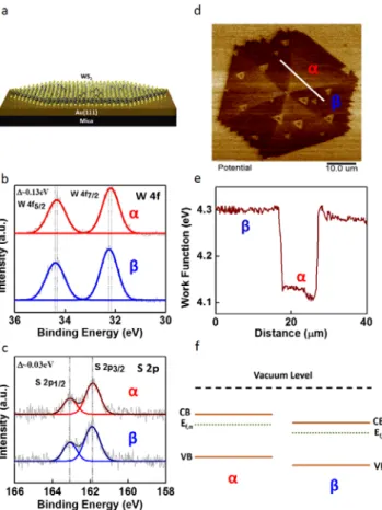
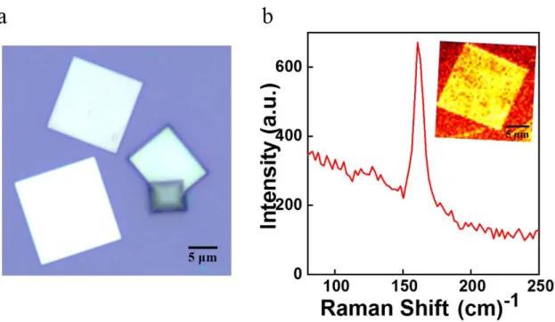
Characterization of monolayer WS 2
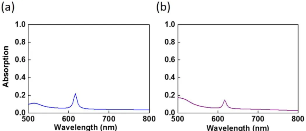
The A-exciton PL peak for the domain is red-shifted relative to the domain. We found that the strain-related E21g mode exhibited a red-shift in the -domain relative to the -domain (0.5 cm1), indicating a tensile strain effect. Similarly, the redshift (1.2 cm-1) of the doping-related A1g state in the -domain relative to the -domain implied carrier doping effects (Figure 4.1 (h)), which was consistent with the observed PL redshift (Figure 4.1(g)).
Stoichiometry and work function of monolayer h-WS 2 single crystal
A schematic representation of the band diagram with the Fermi levels for the and domains relative to the vacuum level is shown in Figure 4.5 (f). Next, using the known value of the Au(111) work function, we performed KPFM measurements with an Al-coated AFM tip on the Au(111)/mica sample to determine the work function of the Al-coated AFM tip. determine Finally, using the known value of the AFM tip work function, we performed KPFM measurements on the h-WS2 monolayer to obtain the spatially resolved work functions associated with the α and β domains, as shown in Fig.
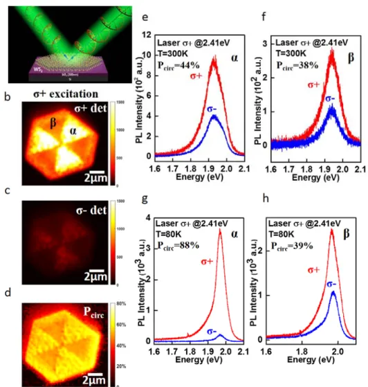
Valley polarization analysis in CVD-grown monolayer WS 2
Circularly polarized emission from monolayer h-WS2 neutral excitons: (a) Schematic of circularly polarized emission on monolayer h-WS2 under + 514nm (2.41 eV) excitation. Similarly, at 80K, the degree of circularly polarized emission in low-defect domains was found to approach ~90%, suggesting nearly perfect valley polarization. Circularly polarized emission of as-grown monolayer h-WS2 under 514.3nm excitation: (a) polarized emission and (b) polarized emission intensity mapping. c) The degree of valley polarization Pcirc.
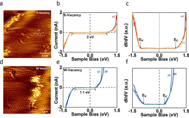
Defect density analysis of the monolayer h-WS 2 by CAFM
The apparent visibility of defect locations in the CAFM maps allowed direct counting of the number of defects in both the and domains. From our experiments, the apparent anti-correlation between the defect density and PL intensity is useful to identify the role of defects in the exciton recombination for monolayer h-WS2. In addition, the large differences in defect density between the and domains gave rise to lower selectivity (ie, less (1)2 ) in the domains.
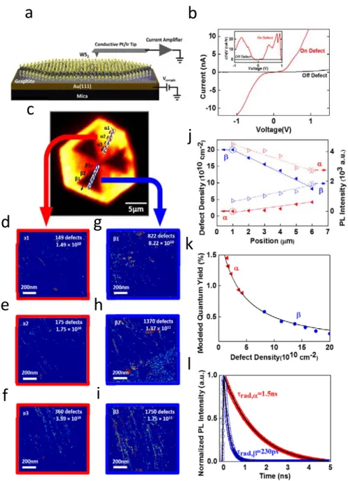
Atomic defects structures analysis of monolayer h-WS 2 by STM
Therefore, the nearly temperature-independent Pcirc in the domain can be understood in terms of the competing effects between increasing (1)2 and decreasing (ex)1 with decreasing temperature according to Eq. For the SV locations of WS2, as illustrated by the white dashed triangles in Figure 4.11(a), the corresponding tunnel conductance spectra were found to be similar to those of vacancy-free areas. The above scenario of higher WV density in the domain is not only consistent with the observation of reduced PL intensities and DOP, but also takes into account the larger work function in the domain (as found by the KPFM studies ) due to the excessive hole doping associated with WVs in WS2.
Summary of synthesis and properties of 2D semiconductor (WS 2 )
The degree of valley polarization (DVP) under circularly polarized light excitation is a parameter that determines the purity of valley polarized photoluminescence (PL) of a WS2 layer. Here, we report that valley-polarized PL of monolayer WS2 can be efficiently tuned at room temperature (RT) through surface plasmon-exciton interaction with plasmonic Archimedean spiral (PAS) nanostructures. Further enhancement and continuous control of the excitonic valley polarization in the electrostatically doped WS2 monolayer are demonstrated.
Introduction
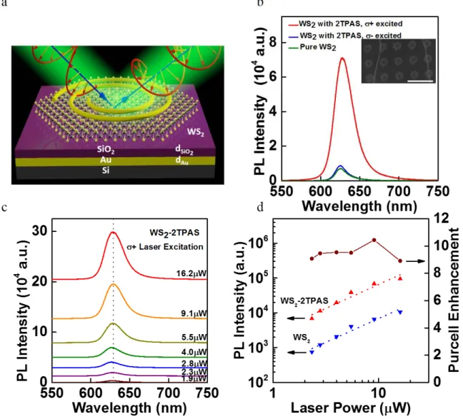
The device configuration consists of a chemical vapor deposition (CVD) grown monolayer WS2 transferred onto a 60 nm thick SiO2 substrate on top of a 150 nm thick gold reflection layer. In comparison, the RT values of the DVP in monolayer WS2-2TPAS and WS2-4TPAS under the excitation of right-handed circularly polarized (RCP) light are found to increase to 40% and 50%, respectively. In contrast, the corresponding values of the DVP under the excitation of left circularly polarized (LCP) light are found to decrease up to 5% in both monolayer WS2-2TPAS and WS2-4TPAS heterostructures.
Device fabrication and actively controlled PL enhancement
Structure and optical spectral properties of single-layer WS2 integrated two-turn (2T) right-handed Archimedean plasmonic coil heterostructures (WS2-2TRHPAS).
Valley polarized PL spectra of pure monolayer WS 2 and WS 2 -2HPAS heterostructure
As shown in Figure 5.2(b), the intensity of the PL emission spectra from the WS2-RHPAS heterostructure is significantly enhanced relative to the intensity of the emission spectra under excitation. In contrast, the PL intensity of the and emission spectra from the WS2-RHPAS heterostructure does not show any increase under excitation, as shown in Fig. 5.2(e). We find that the DVP value from the WS2-2TRHPAS heterostructure increased by ~55% under excitation and decreased by ~1% under excitation.
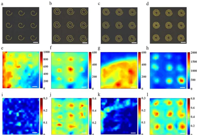
Ring-number dependent valley polarized PL spectra of WS 2 -RHPAS heterostructure
For comparison between the DVP under and excitations, the corresponding DVP spectra are shown in Figures 5.2(c) and 5.2(f) for the as-grown WS2 and the WS2-2TRHPAS heterostructure, respectively. These notable DVP values of the WS2-2TRHPAS can be attributed to the non-trivial interaction between the excitons in WS2 and the chiral plasmonic mode in the PAS. The excitations thus generated (RCP emission) interact constructively with the SPP field, leading to increased PL intensity at the center of the RH spiral structure.
Electrical tuning of the DVP in the WS 2 -2TRHPAS heterostructure
In contrast, for VGate > 0, the integrated intensity of the X peak gradually decreases and that of the X- peak becomes dominant as VGate increases. Additionally, the polarization resolved PL spectra of the 1L-WS2- 2TRHPAS sample under σ+ excitations are shown in Figures 5.4(g) and 5.4(h) for VGate = 10 V and 20 V, respectively. Specifically, we find that the DVP values for VGate = 0, 10 V, and 20 V are 0.4, 0.5, and 0.7, respectively, suggesting significantly enhanced valley polarization as the applied bias is disconnected from the load neutral point. e) Contour plot of PL spectra of 1L-WS2-2TRHPAS as a function of VGate at RT.
Summary
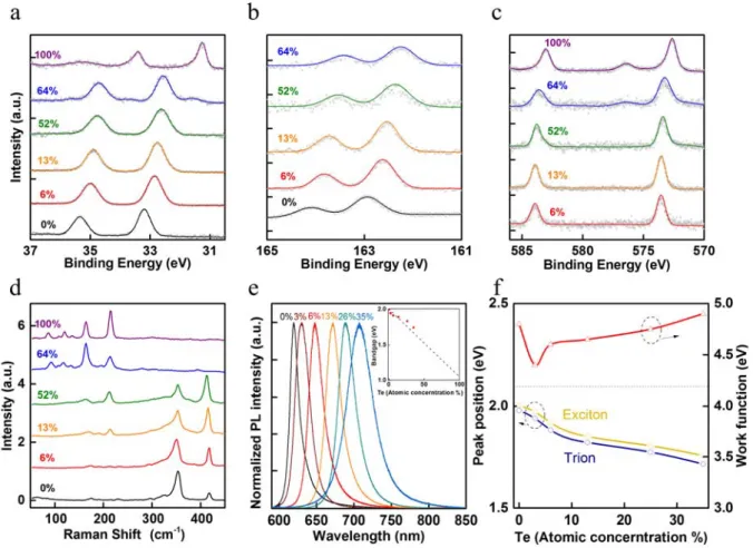
In addition, the use of WTe2 metal contacts with a work function close to the band edge of WTe0.06S1.94. The optical properties of the as-grown WTe2xS2(1-x) alloys were investigated by Raman and PL spectra. In Fig. 6.1d, Raman spectra of WTe2xS2(1-x) alloys with different Te concentrations were collected to study the composition-dependent modes of lattice oscillations.
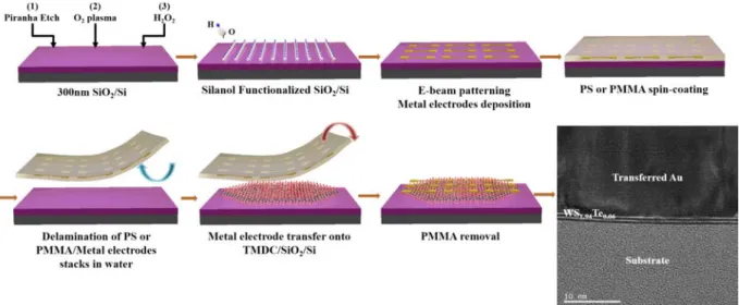
A simple metal electrodes transferred method
Schematic transfer of surface-functionalized water-assisted wafer metal electrodes to the TMDCs: (a) Schematic of the SiO2/Si substrate.
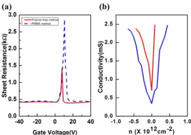
In Figure 6.8(d), the effective SBH was extracted under the flat band gate voltage condition, which corresponded to the onset of derivations from the linear region. Since RT of the WTe0.06S1.94 alloy FET is the sum of the channel resistance and the series resistance (RT = Rsd + RCanal), the Rsd can be extracted using two different channel resistance values at high overdrive bias. Since the contact resistance is exponentially proportional to the height of the Schottky barrier, this reduction in contact resistance is attributed to the reduction in SBH.
Contributions of this thesis
Atomic Resolution Imaging of Grain Boundary Defects in Monolayer Chemical Vapor Deposition-Grown Hexagonal Boron Nitride. In situ synthesis of a large area boron nitride/graphene monolayer/boron nitride film by chemical vapor deposition. Ultraclean and large monolayer hexagonal boron nitride on Cu foil using chemical vapor deposition.
Appendix A1: Experimental setup
Growth conditions for hexagonal single crystalline BLG flakes