I am grateful to the members of my doctoral committee for their constructive contributions to my research. Due to the presence of various competing design goals, analog circuit sizing is incomplete without analyzing the trade-offs between performance specifications.
Introduction
As we know, the construction flow of an analog circuit varies according to applications, usually it can be represented as shown in Figure 1.2. The knowledge and experience of the designer is more important in every phase of analog circuit design.
![Figure 1.1: Comparison of analog and digital design [1]](https://thumb-ap.123doks.com/thumbv2/azpdfnet/10540660.0/27.892.134.753.171.575/figure-1-1-comparison-analog-digital-design-1.webp)
Thesis Motivation and Objective
To address these problems, several multi-objective techniques have been proposed with an emphasis on nature-inspired algorithms due to their inherent capability and efficiency in handling uncertainty during circuit design flow. The aim of this thesis is to develop methodologies for the optimization of analog/RF circuits using sensitivity analysis and metaheuristics.
Thesis Contributions
In order to achieve these goals, the following are the main tasks that must be accomplished. Formulation of the temperature map scheme as an initialization scheme for SA in the hybrid framework.
Thesis Organization
Fundamentals of Optimization Techniques in Analog Circuit Sizing
Sensitivity Analysis and Circuit Optimization
Analog Circuit Optimization using Metaheuristics
Multi-objective Optimization of Analog Circuits using Metaheuris- tics
The performance of proposed algorithms (MHPSO, MHPSO-CD) is evaluated on various test functions and the results are compared with standard multi-objective evolutionary algorithms.
Conclusions and Future Work
Introduction
The analog circuit or sizing optimization problem can be easily expressed as a single or multi-objective optimization problem subject to a set of constraints. Unlike single-objective circuit optimization, multi-objective circuit optimization deals with multiple objective functions simultaneously.
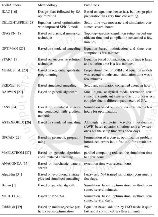
Review of Analog Circuit Sizing Approaches
23] and FASY [24], similar strategy is applied with simulated annealing (SA) and a simulation-based optimization strategy, respectively. b) General problem formulation: Induction of heuristics for analog circuit sizing enables designers to generalize analytical formulation of the optimization problem. Multi-objective optimization: The design and optimization of an analog circuit can be treated as a multi-objective optimization (MOO) problem.
Selected Optimization Methodologies
- Adjoint Network based Sensitivity Analysis (ANSA)
- Particle Swarm Optimization (PSO)
- Simulated Annealing (SA)
- Metaheuristics
The optimal solution can therefore be obtained with the help of SPICE simulations and sensitivity calculations. In the case of circuit optimization, these variables can be the length (L), width (W), and transconductance (gm) of a device (transistor). For a particle in the iteration, if position and velocity are xi and vi respectively, the next position can be expressed as [57].
By iteration, the value of the cost function and the corresponding solution can be expressed asf(xi) and xi, respectively. With the increase in time instancex, change in temperature can be shown using (2.7) [10].
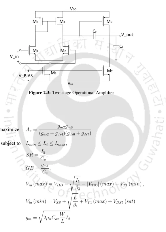
Design Examples
- Two-stage Operational Amplifier : OpAmp
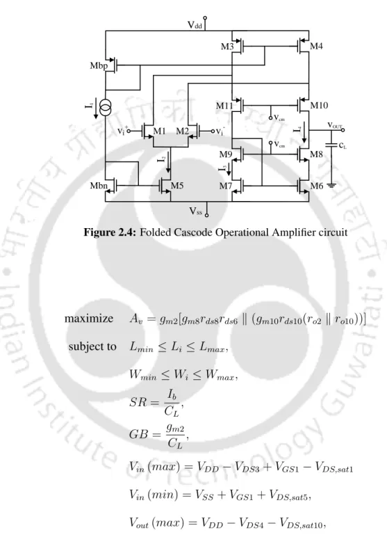
- Folded Cascode Operational Amplifier
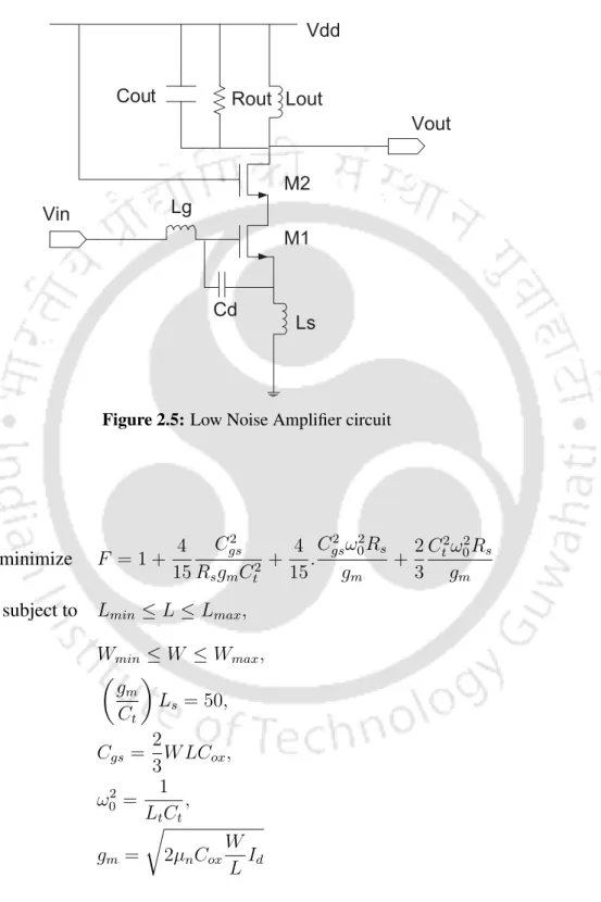
- Low Noise Amplifier : LNA
- Global Solutions
Monomials: When the posinomial consists of only one non-negative term in addition, where t = 1 and c1 ≥ 0, then a monomial function is formed. The design examples explained in this chapter are in the form of a convex formulation since the square law model is used in transistor modeling. The expression takes the non-posinomic form when short-channel effects are included in the transistor model (2.11).
Further, the approximate analytical formulation as shown in (2.12) can be expressed in posinomial/monomial form, after consideration of short-channel effects. In the thesis, to provide a global solution, the square law model for the ANSA method was used.
Summary
This type of problem formulation leads to the convex optimization problem, which after solving provides the global solution. In the case of heuristics (HPSO, l-HPSO, MHPSO, MHPSO-CD), the generation of a global solution is provided by the combination of PSO and SA. Further, to avoid complex analytical formulation, the approximate model of gm as shown in (2.12) is used to incorporate short channel effects and make this solution more accurate.
This chapter presents the technique of analog circuit optimization using adjoint network-based sensitivity analysis (ANSA). ANSA is described in Section 3.2, and the application of ANSA in analog circuit optimization is presented in Section 3.3.
Classical Methods for Sensitivity Analysis
Adjoint Network Based Sensitivity Analysis
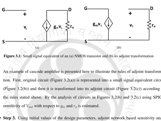
The adjacency network can be represented by transposing the incidence matrix representing a system of equations. The sensitivity of the response of the original network with respect to parameter x can be expressed by a vectorη such that. The original electrical network, where the transistors are represented by their small signal equivalent circuits, is analyzed using Modified Nodal Analysis (MNA) [62].
The formulation in (3.11) can be applied to transistors, transformers and all linear components in the electronic circuit. The adjoint of this circuit can be represented by taking the transpose of the coefficient matrix as shown in (3.11).
Application of Sensitivity Analyses in Analog Circuit Opti- mization
Proposed Methodology
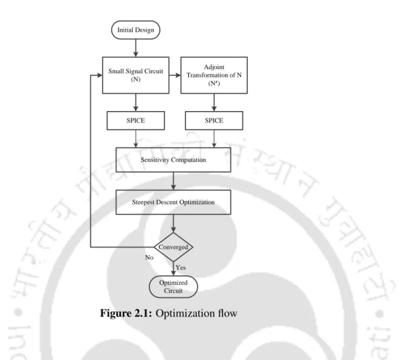
The common transform of the original analog circuit is analyzed by SPICE to estimate the DC operating point. First, the original circuit (Figure 3.2(a)) is represented in a small signal equivalent circuit (Figure 3.2(b)) and then it is transformed into its combined circuit (Figure 3.2(c)) according to the mentioned rules above. Using the initial values of the design parameters, network-based sensitivity analysis is used to evaluate the objective function in the optimal direction through different iterations.
Let the objective function of electrical network be F(Vout,α), where Vout denotes the response of the network and α denotes the vector of the design parameters. In the iteration, sensitivities of Vout with respect to α can be expressed as, . 3.16) where, ∂V∂αoutii is equivalent to the expression given in (3.8) and β is a functional relation between the circuit response and objective function.
Design Examples
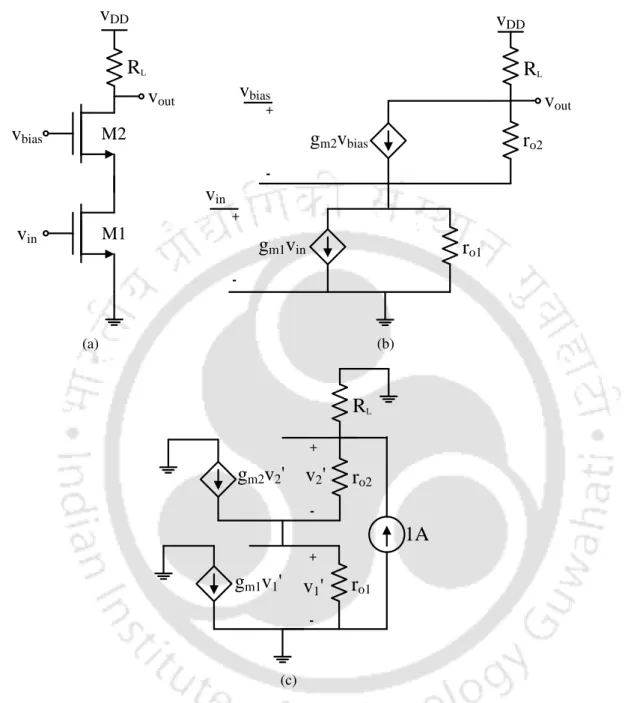
- Cascode Amplifier
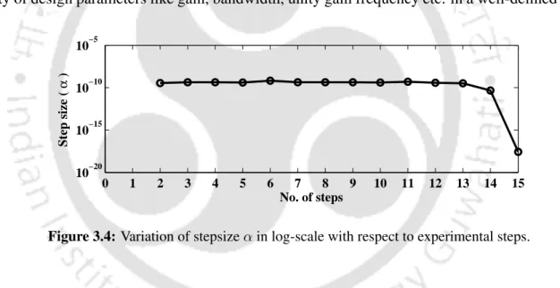
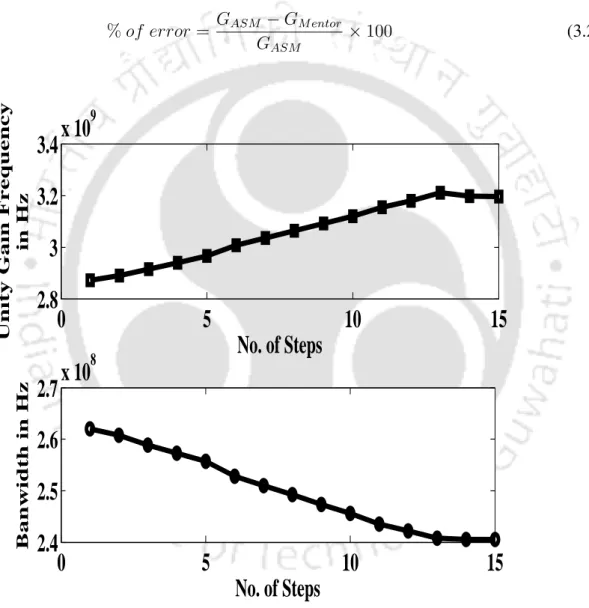
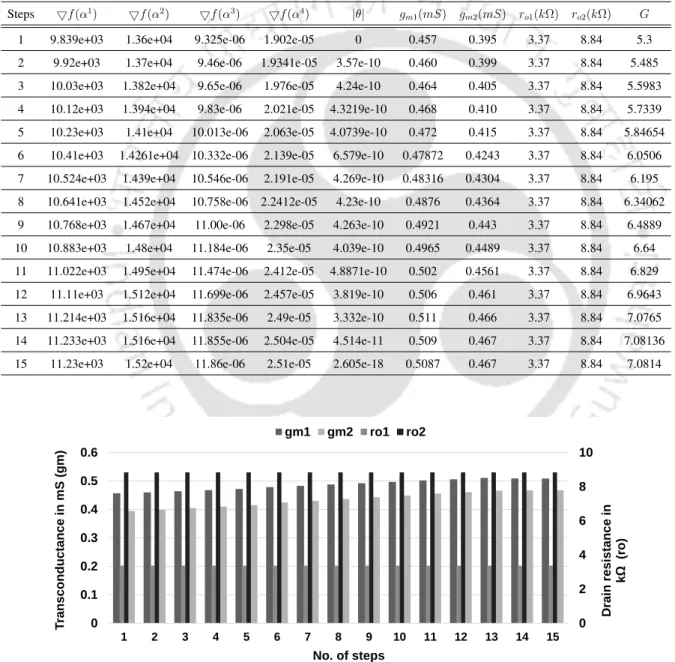
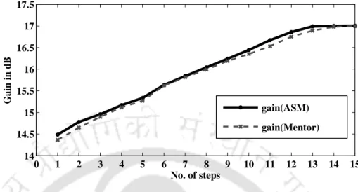
The absolute value of gainG of the amplifier circuit in Figure 3.2(a) can be approximated by the following mathematical equation. It is clear from Figure 3.4 that the step size θ (as shown in step 4) does not change very quickly, causing the design vector to move very smoothly and accurately in an optimal direction. The sensitivity of design parameters to the next iteration is obtained using the gradient of an objective function in each iteration.
For the cascode amplifier circuit in Figure 3.2(a), the design parameters are transconductances and drain-to-source resistances. Since both bandwidth and unity gain frequency can be derived mathematically from transconductance (gm), it is now possible to optimize these two design parameters without even calculating the gradient of objective functions.
No. of Steps
- Two-stage OpAmp Design Optimization
- Summary
- Proposed Hybrid Optimization Approach
- Hybrid Particle Swarm Optimization with L´evy Flight
- Convergence Analysis
- Design Examples
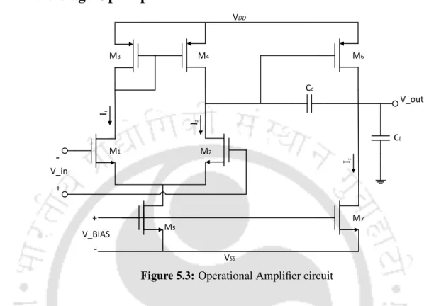
- Design Example 1 : Two-stage Operational Amplifier
- Design Example 2 : Operational Transconductance Amplifier
A two-stage OpAmp shown in Figure 3.7(b) is considered as a test circuit to demonstrate the effectiveness of the proposed approach. Assuming this OpAmp as part of a system that has capacitive loading in the range of a few pico-farads. Capacitor Cc (Miller Capacitance) and resistor R are carefully used for pole and zero compensation, respectively. A two-stage operational amplifier circuit [3] as shown in Figure 4.2 is taken as a benchmark to demonstrate the effectiveness of the proposed approach.
The transconductance vector Gm (gm1, gm2,gm5) is treated as the position of particles for application of the proposed approach. To demonstrate the effectiveness of the proposed approach, a simple OTA circuit, as shown in Figure 4.6, is taken as a design example to be used in a weak or moderate inversion region at long channel lengths.
No. of Iterations
Voltage gain of OTA (dB) 5060
Design Example 3 : Low Noise Amplifier
The schematic of LNA, as shown in figure 4.10, contains two MOSFETs M1 and M2 and a tuning circuit (Cout and Lout) tuned at a center frequency of 2.4GHz. In these cases, SA is applied in the rest of the temperature ranges to search for an optimum solution. Another reason for the absence of particles in a particular temperature region is the distribution of temperature regions based on particle velocities.
Figures 4.11 and 4.12 represent variations in the NF and gain, respectively, at different temperature ranges for a single experiment. Since the objective is to minimize NF gain, above 10dB is maintained and it can be seen from Figure 4.12 that at higher temperature ranges the gain of LNA is higher.
Results
Summary
In this design example, the noise figure is minimized subject to constraints such as input matching, bandwidth, bias, etc. HPSO andl-HPSO results for two-stage OpAmp, folded cascode amplifier and LNA are compared with standard algorithms. The proposed methods are also tested using benchmarks and the performance is compared with peer algorithms.
The results of standard test functions are presented in section 5.4 and chapter is summarized in section 5.5.
Proposed Multi-objective Hybrid Particle Swarm Optimiza- tion (MHPSO)
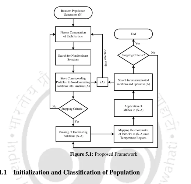
- Initialization and Classification of Population
- Particle Movement and Finding Global-best
- Ranking and Voltage-Temperature (V-T) Mapping Scheme
- Annealing Process
- Niche Preservation
- Computational Complexity
Further, the solutions will be subjected to multi-objective annealing process to search for any remaining non-dominated solutions and obtain a diverse Pareto front. Since the annealing process is applied to dominated solutions after swarm search, the proposed MHPSO procedure maintains a diversity in spaceSN at each generation. While constructing subspaces and performing annealing process in each subspace, it is worth noting that multiple particles (xcount) may have the same temperature values associated with them, or no particles have the same temperature (t).
The subspace with the highest ρ count is subjected to the annealing process to update the archive A. Only some particles undergo the annealing process in the subspace having a low ρ count, i.e. the particles having very low temperature values are discarded .
Setup for Experiments
The first one is about finding the proximity of the obtained solutions with the Pareto front and the second one is about finding diverse solutions with respect to the Pareto front. Therefore, to compare multi-objective evolutionary algorithms (MOEA), at least two performance metrics (one evaluating the proximity of the desired Pareto front, i.e. P?, and the other evaluating the dispersion of the obtained Pareto front) should be needed . used. IGD can be expressed as,. where ntrue is the number of solutions on the real Pareto front, and d0i represents the Euclidean distance between the solutions on the real Pareto front and the nearest solution on it.
The objective is to calculate either area or volume of the objective space covered by the obtained Pareto-optimal solutions. Nevertheless, it can be used in conjunction with GD or IGD metrics to get a better view of an algorithm's performance. iv) Simulation setup: The parameters of peer and proposed algorithms are given in Table 5.1, where N, Ns and A denote the population size, swarm size and archive size respectively.
Optimization of Analog Circuit Design
- Two-stage OpAmp
- Folded cascode OpAmp
- Low Noise Amplifier (LNA)
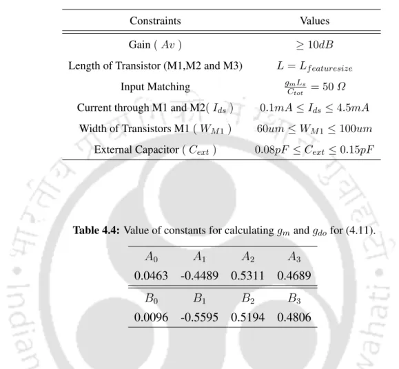
The design problem is formulated as a multi-objective optimization problem using the constraints shown in Table 5.2. Further, comparison between Pareto fronts, generated by proposed algorithms (MHPSO and MHPSO-CD) and other evolutionary algorithms is shown in Figure 5.6. The design problem is formulated as a multi-objective optimization problem using the constraints shown in Table.
Further, the comparison between Pareto fronts generated by proposed algorithms (MHPSO and MHPSO-CD) and other evolutionary algorithms is shown in Figure 5.7. Details of various specifications and constraints during the optimization process are shown in Table 5.5.
Benchmark Results and Analysis
Summary
Lee, “GPCAD: A tool for cmos op-amp synthesis,” in Proceedings of the 1998 IEEE/ACM international conference on computer-aided design. Rodr´ıguez-V´azquez, “A statistical optimization-based approach for automated sizing of analog cells,” in Proceedings of the 1994 IEEE/ACM International Conference on Computer-aided Design, ser. He, “Evolutionary design of an operational amplifier using a variable-length differential evolution algorithm,” in 2010 International Conference on Computer Application and System Modeling (ICCASM 2010), vol.
Horta, “GENOM-POF: Multi-objective evolutionary synthesis of analog ICs with angle validation,” in Proceedings of the 14th Annual Conference on Genetic and Evolutionary Computation, ser. Trivedi, “A method for optimizing analog circuits using adjoint sensitivity analysis,” in 2015, 25th International Radio Electronics Conference (RADIOELEK-TRONIKA), April 2015, pp.
![Figure 1.2: General flow of analog design at circuit-level [2]](https://thumb-ap.123doks.com/thumbv2/azpdfnet/10540660.0/28.892.174.740.173.715/figure-1-general-flow-analog-design-circuit-level.webp)