Machine-Intelligence-Driven High- Throughput Prediction of 2D Charge
Density Wave Phases
Arnab Kabiraj and Santanu Mahapatra*
Nano-Scale Device Research Laboratory, Department of Electronic Systems Engineering, Indian Institute of Science (IISc) Bangalore, Bangalore - 560012, India.
Supporting Information
*Email: [email protected]
S1
Table S1: All CDW materials and their phases, energy differences with the normal phase, and band/CDW-gaps, as found by our computational methodology. Note the convention here. The normal phase is called ɸ0, the CDW phase just less stable than ɸ0 is called ɸ-1, and the phase just less stable than ɸ-1 is named ɸ-2, and so on. Two numbers are in parenthesis beside the ɸ names.
The first value denotes the energy difference of that CDW phase with its corresponding normal phase in units of meV/formula unit. The second value states the band/CDW-gap of that CDW phase in units of eV. The CDW-gaps are marked with an asterisk (blue font) while the proper band gaps (red font) are not. For example, the notation ɸ-2 (-26.52, 0.5*) for √13×√13 periodicities of TaS2-T means that this is the 2nd CDW phase found in this periodicity by descending order (lower energy is more stable), the phase is more stable than the normal phase by 26.52 meV/formula-unit and it has a 0.5 eV CDW-gap.
Material 2×2 3×3 √13×√13 4×4
TaS2-T No phase ɸ-1 (-12, 0) ɸ-1 (-13.96, 0) ɸ-2 (-26.52, 0.5*)
ɸ-1 (-17.61, 0)
TaS2-H No phase ɸ-1 (-3.92, 0) ɸ-1 (-0.22, 0) ɸ-2 (-0.7, 0)
ɸ-1 (-0.42, 0) ɸ-2 (-1.16, 0) Hf3Te2 ɸ-1 (-2.26, 0) ɸ-2 (-2.43, 0) NA ɸ-1 (-0.66, 0) ɸ-2 (-2.72, 0) LaGeI ɸ-1 (-1.62, 0) No phase No phase ɸ-1 (-2.66, 0)
LaI2 No phase ɸ-1 (-0.64, 0) NA No phase
NbS2-T No phase ɸ-1 (-9.6, 0) ɸ-1 (-38.56, 0.48*) ɸ-1 (-14.11, 0) NbS2-H ɸ-1 (-0.43, 0)
ɸ-2 (-1.05, 0) ɸ-3 (-2.77, 0)
ɸ-1 (-0.71, 0) ɸ-1 (-0.79, 0)
No phase ɸ-1 (-3.9, 0)
NbSe2-T No phase ɸ-1 (-36.21, 0) ɸ-1 (-68.85, 0) ɸ-1 (-33.54, 0) NbSe2-H ɸ-1 (-0.22, 0)
ɸ-2 (-1.05, 0)
ɸ-1 (-2.18 0) ɸ-2 (-2.69, 0)
ɸ-2 (-2.9, 0)
ɸ-1 (-3.31, 0) ɸ-1 (-1.78, 0) ɸ-2 (-3.59, 0) ɸ-3 (-4.18, 0) NbTe2-T No phase ɸ-1 (-87.24, 0) ɸ-1 (-93.44, 0) ɸ-1 (-93.2, 0)
S2 ɸ-2 (-111.52, 0)
NbTe2-H ɸ-1 (-2.02, 0) ɸ-1 (-16.81, 0) ɸ-1 (-1.08, 0.16*) ɸ-2 (-4.85, 0.25*)
ɸ-1 (-25.08, 0)
OsOCl2 ɸ-1 (-0.58, 0) No phase NA No phase
RuOCl2 ɸ-1 (-0.13, 0) No phase NA No phase
TaSe2-T No phase ɸ-1 (-43.18, 0) ɸ-1 (-67.38, 0.57*) ɸ-1 (-34.95, 0) TaSe2-H ɸ-1 (-0.83, 0)
ɸ-2 (-1.93, 0)
ɸ-1 (-7.16, 0) ɸ-2 (-8.35, 0) ɸ-3 (-8.75, 0)
ɸ-1 (-5.72, 0) ɸ-1 (-3.2, 0)
TaTe2-T No phase ɸ-1 (-128.98, 0) ɸ-1 (-5.44, 0) ɸ-1 (-120.72, 0) TaTe2-H ɸ-1 (-6.37, 0)
ɸ-2 (-11.97, 0)
ɸ-1 (-18.8, 0) ɸ-2 (-23.46, 0)
No phase ɸ-1 (-22.82, 0)
Ti2PTe2 ɸ-1 (-1.14, 0) ɸ-1 (-1.31, 0)
No phase No phase No phase
TiBr2 ɸ-1 (-351.36, 0.34) ɸ-1 (-178.64, 0) ɸ-2 (-284.93, 0.41)
ɸ-1 (-286.9, 0.18) ɸ-1 (-353.97, 0.34) repeat of 2×2 TiCl2 ɸ-1 (-321.45, 0.38) ɸ-1 (-120.01, 0)
ɸ-2 (-216.19, 0.44)
ɸ-1 (-232.63, 0.15) ɸ-1 (-324.81 0.38) repeat of 2×2 TiOBr ɸ-1 (-5.59, 0)
ɸ-2 (-10.86, 0)
ɸ-1 (-12.84, 0) NA ɸ-1 (-11.78, 0)
TiOCl ɸ-1 (-7.31, 0) ɸ-2 (-13.37, 0)
ɸ-1 (-13.6, 0) NA ɸ-1 (-20.33, 0.09)
TiS2 ɸ-1 (-5.76, 0.25) ɸ-1 (-2.54, 0.15) No phase ɸ-1 (-4.64, 0.25) repeat of 2×2 TiSe2 ɸ-1 (-4.55, 0) ɸ-1 (-0.11, 0) No phase ɸ-1 (-6.73, 0) TiTe2 ɸ-1 (-0.93, 0) No phase No phase ɸ-1 (-0.33, 0) VOCl ɸ-1 (-105.63, 0)
ɸ-2 (-154.42 0.14)
ɸ-1 (-145.87, 0) NA ɸ-1 (-140.91, 0.14) repeat of 2×2 ZrTe2 ɸ-1 (-0.16, 0)
ɸ-2 (-0.82, 0)
ɸ-1 (-0.53, 0) ɸ-1 (-0.41, 0) ɸ-1 (-0.27, 0)
S3 ZrTe3 ɸ-1 (-0.77, 0)
ɸ-2 (-1.39, 0)
ɸ-1 (-1.1, 0) NA ɸ-1 (-0.27, 0)
ZrTiSe4 ɸ-1 (-4, 0.25) ɸ-1 (-0.14, 0) ɸ-2 (-0.58, 0)
NA ɸ-1 (-4.43, 0.25) repeat of 2×2 ZrTiTe4 ɸ-1 (-4.29, 0) ɸ-1 (-0.47, 0) NA ɸ-1 (-4.82, 0)
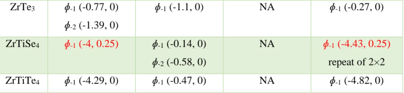
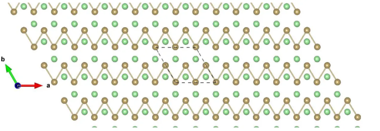
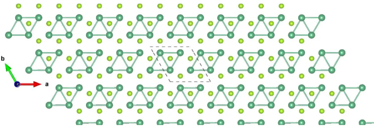
Figure S1: Top view of TaS2-T 3×3 ɸ-1. The brown and yellow balls represent the Ta and S atoms, respectively.
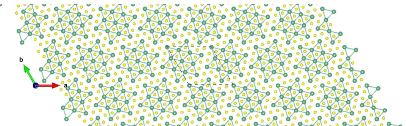
Figure S2: Top view of TaS2-T √13×√13 ɸ-1.
S4 Figure S3: Top view of TaS2-H 3×3 ɸ-1.
Figure S4: Top view of TaS2-H 4×4 ɸ-1.
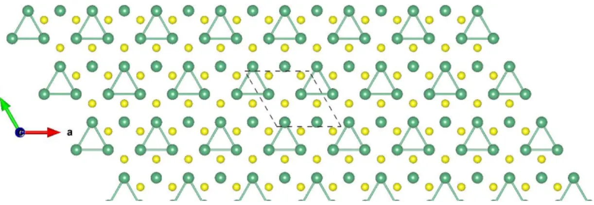
Figure S5: Top view of TaSe2-T 3×3 ɸ-1. The brown and green balls represent the Ta and Se atoms, respectively.
S5 Figure S6: Top view of TaSe2-T √13×√13 ɸ-1.
Figure S7: Top view of TaSe2-T 4×4 ɸ-1.
Figure S8: Top view of TaSe2-H 2×2 ɸ-1.
S6 Figure S9: Top view of TaSe2-H 2×2 ɸ-2.
Figure S10: Top view of TaSe2-H 3×3 ɸ-1.
Figure S11: Top view of TaSe2-H 3×3 ɸ-2.
S7 Figure S12: Top view of TaSe2-H 3×3 ɸ-3.
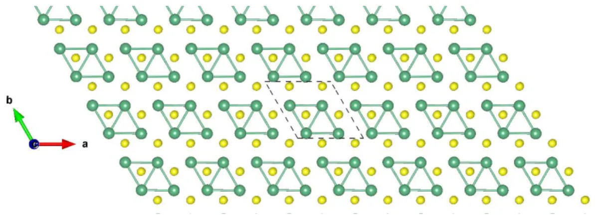
Figure S13: Top view of TaTe2-H 2×2 ɸ-1. The brown and dark green balls represent the Ta and Te atoms, respectively.
Figure S14: Top view of TaTe2-H 2×2 ɸ-2.
S8 Figure S15: Top view of TaTe2-H 3×3 ɸ-1.
Figure S16: Top view of TaTe2-H 3×3 ɸ-2.
Figure S17: Top view of TaTe2-H 4×4 ɸ-1.
S9
Figure S18: Top view of NbS2-H 2×2 ɸ-1. The dark green and yellow balls represent the Nb and S atoms, respectively.
Figure S19: Top view of NbS2-H 2×2 ɸ-2.
Figure S20: Top view of NbS2-H 2×2 ɸ-3.
S10 Figure S21: Top view of NbS2-H 3×3 ɸ-1.
Figure S22: Top view of NbS2-H 3×3 ɸ-2.
Figure S23: Top view of NbS2-T 3×3 ɸ-1.
S11 Figure S24: Top view of NbS2-T √13×√13 ɸ-1.
Figure S25: Top view of NbS2-T 4×4 ɸ-1.
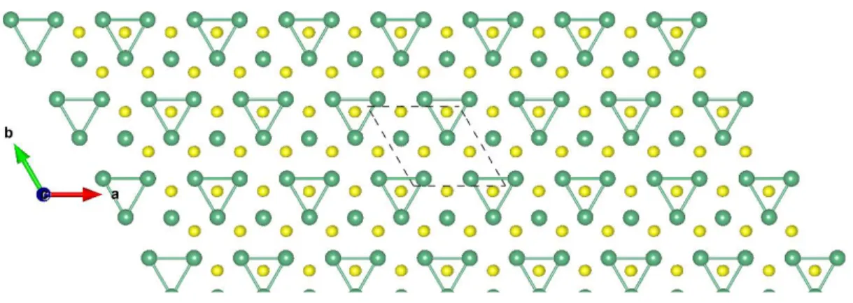
Figure S26: Top view of NbSe2-H 2×2 ɸ-1. The dark and light green balls represent the Nb and Se atoms, respectively.
S12 Figure S27: Top view of NbSe2-H 2×2 ɸ-2.
Figure S28: Top view of NbSe2-T 3×3 ɸ-1.
Figure S29: Top view of NbSe2-T √13×√13 ɸ-1.
S13
Figure S30: Top view of NbTe2-H 2×2 ɸ-1. The dark green and brown balls represent the Nb and Se atoms, respectively.
Figure S31: Top view of NbTe2-H 3×3 ɸ-1.
Figure S32: Top view of NbTe2-H √13×√13 ɸ-1.
S14 Figure S33: Top view of NbTe2-H √13×√13 ɸ-2.
Figure S34: Top view of NbTe2-H 4×4 ɸ-1.
Figure S35: Top view of NbTe2-T 3×3 ɸ-1.
S15 Figure S36: Top view of NbTe2-T 3×3 ɸ-2.
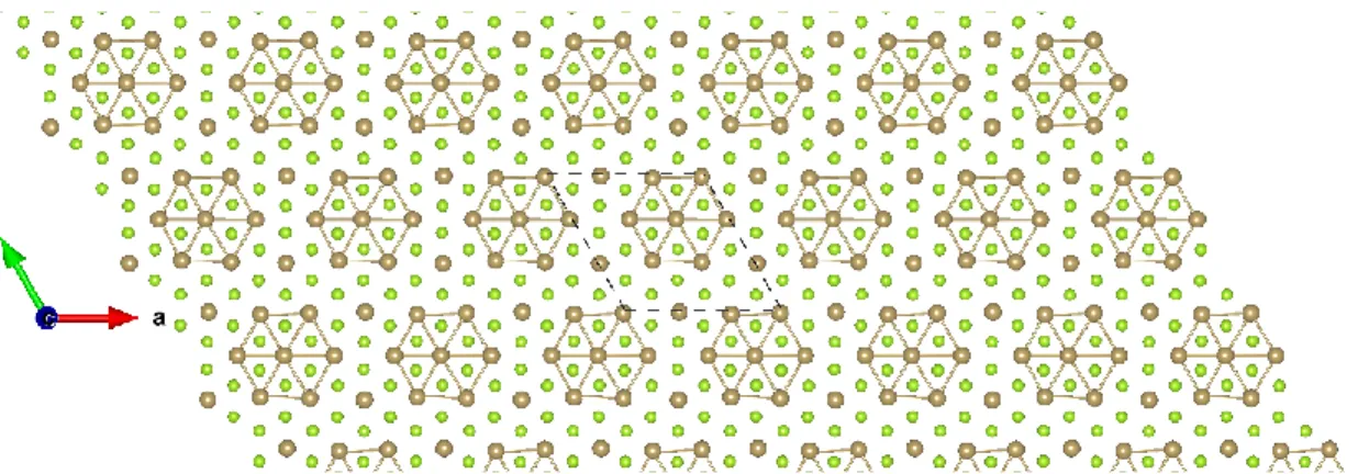
Figure S37: Top view of LaGeI 2×2 ɸ-1. The dark green, blue and purple balls represent the La, Ge, and I atoms, respectively.
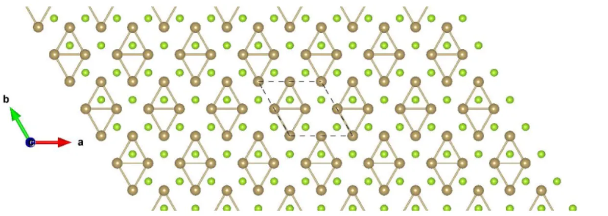
Figure S38: Top view of TiBr2 2×2 ɸ-1. The sky blue and brown balls represent the Ti and Br atoms, respectively.
S16 Figure S39: Top view of TiBr2 3×3 ɸ-1.
Figure S40: Top view of TiBr2 3×3 ɸ-2.
Figure S41: Top view of TiBr2 √13×√13 ɸ-1.
S17
Figure S42: Top view of TiCl2 3×3 ɸ-1. The sky blue and green balls represent the Ti and Cl atoms, respectively.
Figure S43: Top view of TiCl2 3×3 ɸ-2. The sky blue and green balls represent the Ti and Cl atoms, respectively.
Figure S44: Top view of TiOBr 2×2 ɸ-1. The sky blue, red, and brown balls represent the Ti, O, and Br atoms, respectively.
S18 Figure S45: Top view of TiOBr 2×2 ɸ-2.
Figure S46: Top view of TiOBr 3×3 ɸ-1.
Figure S47: Top view of TiOBr 4×4 ɸ-1.
S19
Figure S48: Top view of TiOCl 3×3 ɸ-1. The sky blue, red, and green balls represent the Ti, O, and Cl atoms, respectively.
Figure S49: Top view of TiOCl 4×4 ɸ-1.
Figure S50: Top view of TiS2 2×2 ɸ-1. The sky blue and yellow balls represent the Ti and S atoms, respectively.
S20 Figure S51: Top view of TiS2 3×3 ɸ-1.
Figure S52: Top view of TiSe2 3×3 ɸ-1. The sky blue and light green balls represent the Ti and Se atoms, respectively.
Figure S53: Top view of VOCl 2×2 ɸ-1. The royal blue, red, and light green balls represent the V, O, and Cl atoms, respectively.
S21 Figure S54: Top view of VOCl 2×2 ɸ-2.
Figure S55: Top view of VOCl 3×3 ɸ-1.
Figure S56: Top view of ZrTe2 2×2 ɸ-1. The orange and green balls represent the Zr and Te atoms, respectively.
S22 Figure S57: Top view of ZrTe2 2×2 ɸ-2.
Figure S58: Top view of ZrTe3 2×2 ɸ-1. The same color convention of the last 2 Figures has been used.
Figure S59: Top view of ZrTe3 2×2 ɸ-2.
S23 Figure S60: Top view of ZrTe3 3×3 ɸ-1.
Figure S61: Top view of ZrTiSe4 3×3 ɸ-1. The orange, blue, and green balls represent the Zr, Ti and Se atoms, respectively.
Figure S62: Top view of ZrTiSe4 3×3 ɸ-2.
S24
Figure S63: Band structure of 1T-TaS2 √13×√13 ɸ-2 (CCDW). Note that for this and all subsequent band structures, the supercell band structure is presented and thus, the effect of BZ folding is included.
S25 Figure S64: Band structure of 1T-TaSe2 √13×√13 ɸ-1.
S26 Figure S65: Band structure of 1T-NbSe2 √13×√13 ɸ-1.
S27 Figure S66: Band structure of 2H-NbTe2 √13×√13 ɸ-1.
S28 Figure S67: Band structure of 2H-NbTe2 √13×√13 ɸ-2.
S29 Figure S68: Band structure of TiBr2 2×2 ɸ-1.
S30 Figure S69: Band structure of TiBr2 3×3 ɸ-2.
S31 Figure S70: Band structure of TiBr2 √13×√13 ɸ-1.
S32 Figure S71: Band structure of TiCl2 2×2 ɸ-1.
S33 Figure S72: Band structure of TiCl2 3×3 ɸ-2.
S34 Figure S73: Band structure of TiCl2 √13×√13 ɸ-1.
S35 Figure S74: Band structure of TiOCl 4×4 ɸ-1.
S36 Figure S75: Band structure of TiS2 2×2 ɸ-1.
S37 Figure S76: Band structure of TiS2 3×3 ɸ-1.
S38 Figure S77: Band structure of VOCl 2×2 ɸ-2.
S39 Figure S78: Band structure of ZrTiSe4 2×2 ɸ-1.
S40
Computational Methods
DFT calculations are carried out using the generalized gradient approximation(GGA) as implemented in the code VASP1–4 with the PAW5 method using the Perdew−Burke−Ernzenhof (PBE)6 exchange-correlation functional. The pseudopotentials recommended by VASP have been used throughout. Sufficiently large cutoff energy of 550 eV is used to avoid any Pulay stress. For all structural relaxations, a > 30
𝑎 ×30
𝑏 × 1 Gamma-centered k-points grid is used to sample the Brillouin zone, where a and b are the lattice parameters of the particular supercell. A > 60
𝑎 ×60
𝑏 × 1 similar k-mesh is used for all static runs. The charge densities generated by these static runs have been used to perform the non-self-consistent band structure runs. Electronic convergence is set to be attained when the difference in energy of successive electronic steps becomes less than 10-6 eV, whereas the structural geometry is optimized until the maximum Hellmann–Feynman force on every atom falls below 0.01 eV/Å. A large vacuum space of ≥ 25 Å in the direction of c is applied to avoid any spurious interaction between periodically repeated layers.
For the ZrTiSe4 Fermi surface calculation, the code QuantumATK7 has been used in conjunction with the PBE functional, where the accuracy of the calculations mostly depends on the selection of norm-conserving pseudopotentials and numerical LCAO basis sets. The “SG15” norm- conserving pseudopotentials with “Medium” basis sets have been used. The optimized “SG15”
provides smooth pseudopotentials with multiple projectors and non-linear core corrections8,9. A 7×13×1 k-points sampling and cutoff energy of 75 Hartree has been employed for both structural relaxation, and band structure/Fermi-surface calculation. The obtained relaxed crystal and band structure is found to be almost identical to those produced by VASP, establishing transferability of the results across different DFT codes and methods.
Phonon calculations are done using the code Phonopy10, which uses the atomic forces calculated by VASP based on finite displacement method applied to 2×2 magnified cells employing a >
60 𝑎 ×60
𝑏 × 1 k-mesh and 10-8 eV electronic convergence criteria.
The “Shake & Relax” protocol of the package AIRSS11 interfaced with VASP has been used to produce the distorted structures. A minimum separation of 2 Å is kept between all atoms to minimize unphysical atomic overlaps. The same rigorous DFT relaxation criteria mentioned before
S41
have been implemented here. The AIRSS Shake & Relax algorithm and its highly parallel master- slave implementation are similar to that of our previous works12,13. To accelerate the DFT calculations, hardware-accelerators have been employed extensively. GPU version of VASP code14,15 is used, and regular CPU code is adapted for execution in Xeon-Phi (KNL)16.
To generate inputs, parse outputs and measure the RMS displacements, which have been taken as the measure of distortion, the package pymatgen17 is employed. The “Mean-shift” algorithm as implemented in the package scikit-learn18 is used to perform the unsupervised clustering. The bandwidth for the clustering process has been obtained with the “estimate_bandwidth” function which takes two inputs, the data-set and a quantile value (0.3-0.45). The band structure unfolding has been performed with the tool vaspkit19 interfaced with VASP. All crystal-structure images are generated using the tool VESTA20.
All CDW crystal structure files (cif) and their top-view images (png) are available at the OSF repository. (https://osf.io/by7et).
Supporting References
(1) Kresse, G.; Hafner, J. Ab Initio Molecular Dynamics for Liquid Metals. Phys. Rev. B 1993, 47 (1), 558–561.
(2) Kresse, G.; Hafner, J. Ab Initio Molecular-Dynamics Simulation of the Liquid-Metal-- Amorphous-Semiconductor Transition in Germanium. Phys. Rev. B 1994, 49 (20), 14251–
14269.
(3) Kresse, G.; Furthmüller, J. Efficient Iterative Schemes for Ab Initio Total-Energy Calculations Using a Plane-Wave Basis Set. Phys. Rev. B 1996, 54 (16), 11169–11186.
(4) Kresse, G.; Furthmüller, J. Efficiency of Ab-Initio Total Energy Calculations for Metals and Semiconductors Using a Plane-Wave Basis Set. Comput. Mater. Sci. 1996, 6 (1), 15–
50.
(5) Kresse, G.; Joubert, D. From Ultrasoft Pseudopotentials to the Projector Augmented- Wave Method. Phys. Rev. B 1999, 59 (3), 1758–1775.
S42
(6) Perdew, J. P.; Burke, K.; Ernzerhof, M. Generalized Gradient Approximation Made Simple. Phys. Rev. Lett. 1996, 77 (18), 3865–3868.
(7) QuantumATK with Virtual NanoLab, Synopsys Denmark, https://www.synopsys.com/silicon/quantumatk.html
(8) Hamann, D. R. Optimized Norm-Conserving Vanderbilt Pseudopotentials. Phys. Rev. B - Condens. Matter Mater. Phys. 2013, 88 (8), 085117.
(9) Schlipf, M.; Gygi, F. Optimization Algorithm for the Generation of ONCV Pseudopotentials. Comput. Phys. Commun. 2015, 196, 36–44.
(10) Togo, A.; Tanaka, I. First Principles Phonon Calculations in Materials Science. Scr.
Mater. 2015, 108, 1–5.
(11) Needs, C. J. P. and R. J. Ab Initio Random Structure Searching. J. Phys. Condens. Matter 2011, 23 (5), 53201.
(12) Kabiraj, A.; Mahapatra, S. High-Throughput First-Principles-Calculations Based Estimation of Lithium Ion Storage in Monolayer Rhenium Disulfide. Commun. Chem.
2018, 1 (1), 81.
(13) Kabiraj, A.; Mahapatra, S. Intercalation-Driven Reversible Switching of 2D Magnetism. J.
Phys. Chem. C 2020, 124 (1), 1146–1157.
(14) Hacene, M.; Anciaux-Sedrakian, A.; Rozanska, X.; Klahr, D.; Guignon, T.; Fleurat- Lessard, P. Accelerating VASP Electronic Structure Calculations Using Graphic Processing Units. J. Comput. Chem. 2012, 33 (32), 2581–2589.
(15) Hutchinson, M.; Widom, M. VASP on a GPU: Application to Exact-Exchange
Calculations of the Stability of Elemental Boron. Comput. Phys. Commun. 2012, 183 (7), 1422–1426.
(16) Zhao, Z.; Marsman, M.; Wende, F.; Kim, J. Performance of Hybrid MPI / OpenMP VASP on Cray XC 40 Based on Intel Knights Landing Many Integrated Core Architecture. CUG Conference proceedings 2015.
(17) Ong, S. P.; Richards, W. D.; Jain, A.; Hautier, G.; Kocher, M.; Cholia, S.; Gunter, D.;
S43
Chevrier, V. L.; Persson, K. A.; Ceder, G. Python Materials Genomics (Pymatgen): A Robust, Open-Source Python Library for Materials Analysis. Comput. Mater. Sci. 2013, 68, 314–319.
(18) Pedregosa, F.; Varoquaux, G.; Gramfort, A.; Michel, V.; Thirion, B.; Grisel, O.; Blondel, M.; Prettenhofer, P.; Weiss, R.; Dubourg, V.; Vanderplas, J.; Passos, A.; Cournapeau, D.;
Brucher, M.; Perrot, M.; Duchesnay, E. Scikit-Learn: Machine Learning in Python. J.
Mach. Learn. Res. 2011, 12, 2825–2830.
(19) Wang, V.; Xu, N.; Liu, J. C.; Tang, G.; Geng, W.-T. VASPKIT: A Pre- and Post- Processing Program for VASP Code.arXiv:1908.08269 2019.
(20) Momma, K.; Izumi, F. VESTA3 for Three-Dimensional Visualization of Crystal, Volumetric and Morphology Data. J. Appl. Crystallogr. 2011, 44 (6), 1272–1276.