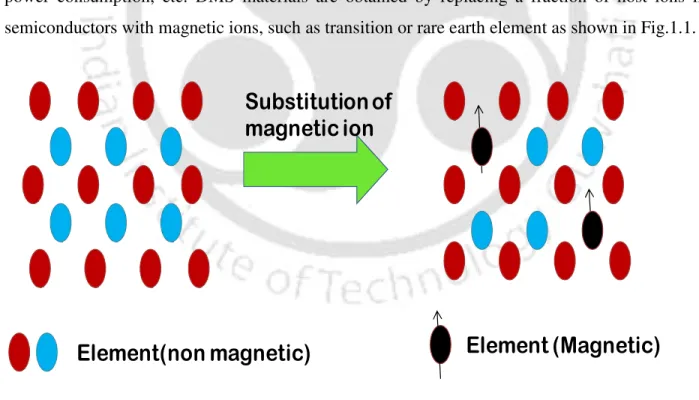
Diluted Magnetic Semiconductors in Spintronics
Enhanced Zeeman Splitting
In the presence of an external magnetic field, the degeneracy of electrons is canceled due to the interaction between the spin of electrons in the material and the magnetic field. This results in a massive Zeeman splitting of the conduction electrons, which is quite large compared to the conventional Zeeman effect in non-magnetic semiconductors[15, 48].
Spin Field Effect Transistor(Spin FET)
Photo Induced Ferromagnet
Spin-LED
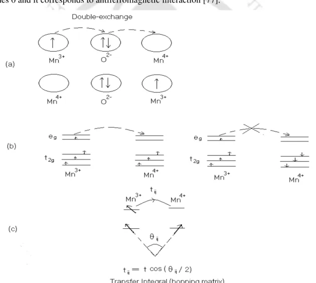
Net rotation for the strong field. The effective magnetic moment of an ion is calculated following Hund. 1.14 (a) Sketch of the double exchange mechanism involving two Mn ions and one O ion. b) Mobility of e.g. of electrons is described for parallel alignment of localized spins. For example, by increasing the Mn concentration from 2.2 to 30%, it was found that the magnetic moment per Mn atom drops from 4.8µB to 0.02µB [193]. FM Tc was found to be above room temperature for Mn.
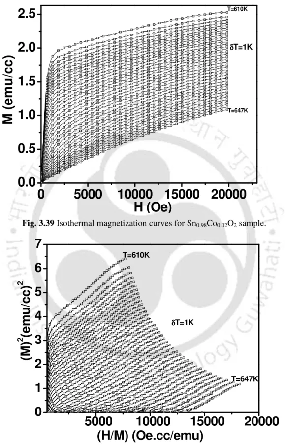
According to the calculation of Wang et al. [45], the presence of vacancies increases the magnetic moment of the TM ion. The calculations performed by Wang et al. show that without the presence of oxygen vacancy, .. the magnetic moment in 12.5 at % co-doped SnO2 is found to be of the order of 0.8 µB/Co-ion and that the value was found to be 2.3 µB/Co-ion by including the vacancy in the. For sample S1, in addition to the negative peak at high temperature, a broad negative peak-like structure is observed at T < 700 K. The low-temperature transition is smeared due to the presence of a dominant transition at high temperature and their possible overlap.
3.42 (a) Spontaneous magnetization (MS) as a function of temperature. b) Graph in logarithmic scale together with adjusted data.
Structural Properties
Crystal Structure
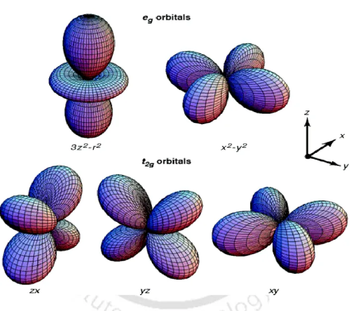
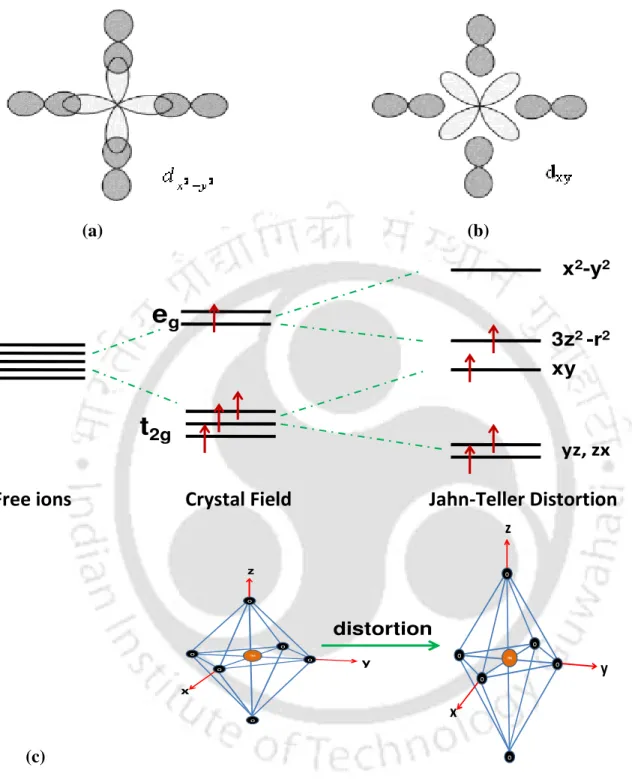
Crystal Field Effect in TM-ion
This effect is clearly seen in the splitting of the energy levels for the five d orbitals. 3d electrons will first fill between the energy of the crystal field and pairing In the presence of a weak crystal in the orbitals will take place according to Hund's rule, i.e.
Jahn-Teller Distortion
This induces a voltage in the pick-up coils which is proportional to the sample's magnetic moment. The critical exponents for the present sample are found to be comparable to those for DMS alloy (Ge,Mn)Te [143], however, they differ from the values corresponding to (Cd,Mn)Sb and (Cd,Mn)Te [144, 145].
Magnetic Ordering
Diamagnetism
Diamagnetism is a fundamental property of materials that try to resist an applied magnetic field, but it is usually very weak. However, when exposed to a magnetic field, the electrons are oriented in such a way that they try to oppose the applied magnetic field and thus they register negative magnetization and negative susceptibility.
Paramagnetism
If N is the number of atoms per unit volume, the volume magnetization M can be written as,.
Ferromagnetism
A related term is saturation magnetization and is the maximum induced magnetic moment per unit volume that can be obtained in a magnetic field (Hsat); beyond this field, no further increase in magnetization can occur. So the total magnetic field experienced by each dipole is the sum of the applied field Ba and the molecular field Bm.
Antiferromagnetism
Ferrimagnetism
Spin Glass Behavior
Magnetic Interactions
- Magnetic Dipole-Dipole Interaction
- Direct Exchange Interaction
- Superexchange Interaction
- RKKY Interaction
- Anisotropic Exchange Interaction
- Double Exchange Interaction
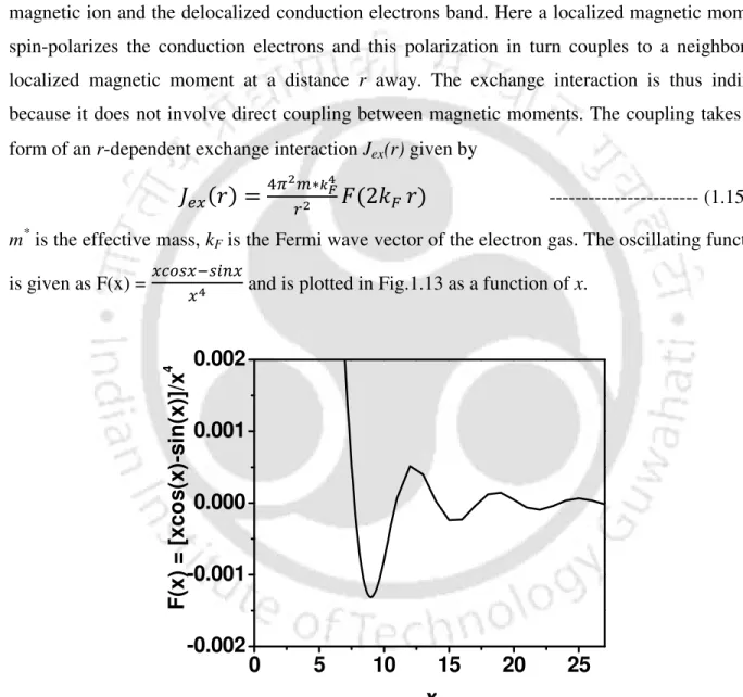
The above type of bond formation cannot occur if the spins of the cations are parallel. F(x) is proportional to the product of the Fermi wave vector and the distance from the localized moment.
Theoretical Models in DMS
Zener Model
Bound Magnetic Polarons
Here, K/ is the exchange constant of ionic carriers in the interstitial region (region between polaronic pairs) and K is the exchange constant of intrapolaronic ionic carriers. Here, M0 = Nms, N is the number of BMPs involved and ms is the effective spontaneous moment on the BMP.
Spin Split impurity band model
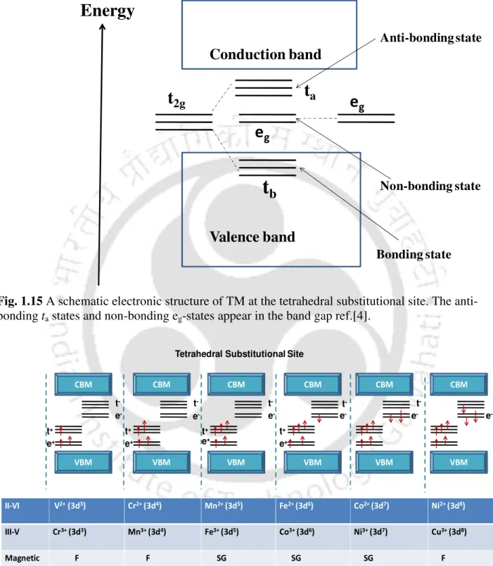
The electronic structure required for high Curie temperature together with the electronic structure for low Curie temperature is shown in Fig. Towards the end of the series, the 3d↓ levels overlap with the impurity band causing high Tc, i.e. The band pattern explains the high Tc observed in TM-doped oxide semiconductors.
Critical Exponents in Magnetic Transition
The list of critical exponents γ, β and δ predicted by various theoretical models is given below. The reported values of critical exponents in various colossal perovskite magnetoresistive materials are found to be different from the values corresponding to long- and short-range FM interactions. However, the values of the critical exponents corresponding to (Cd,Mn)Sb and (Cd,Mn)Te indicate the nearest neighbor Heisenberg interaction.
Electrical Resistivity of Semiconductors
Efros and Skhlovskii (ES) [149] modified the Mott-VRH model to take into account the Coulomb interaction between charge carriers and the corresponding resistance expression is, . Resistivity data were analyzed based on a combination of the thermal excitation model and the Mott-VRH model. Here, A and B are constants, Ed is the activation energy, and C is a constant related to the localized and hopping radii around the localized states.
Experimental Work on Oxide based DMS
Theodoropoulou et al.[199] reported FM with Tc~ 250 K in Mn implanted (3%) single crystal sample of Sn-doped ZnO. A giant magnetic moment of 6.1 µB/Co ion with a high Curie temperature of 790 K was reported by Song et al.[47] on Co-doped ZnO deposited on dielectric LiNbO3. The highest Ms value of 1.7µB/Co ion was measured by Stampe et al.[211] in 7 at % Co-doped sample on LaAlO3 substrate.
Motivation of the present thesis work
The FM Tc was found to be quite large and well above room temperature. In addition to the transition element doping, the oxygen vacancy was found to play an important role in the observed FM behavior. The critical behavior was studied from the detailed magnetization measurement in the vicinity of transition temperature and the estimated critical exponent values were found to be comparable to the Mean Field model prediction.
Experimental Techniques
Sample Preparation
- Solid state reaction
- Mechanical Alloying Technique
- Co-precipitation Technique
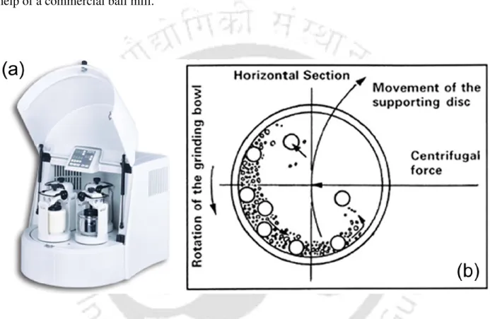
This causes the balls to collide with themselves and the wall of the bottle with high impact. Mixing the starting compounds together with the balls in the vial are subjected to repeated cold welding and breaking on the surfaces of the balls and the vial. The nature of the grinding bottle, balls and grinding media play an important role in the mechanical bonding process.
High Temperature Furnaces
The addition of NH3 was stopped when the pH of the solution reached 12, during which time precipitation has ceased. Finally, the crystalline Co-doped SnO2 powder was dried in an oven at 80ºC for several hours. An external on/off relay (15A capacity) was used to control the power supply to the heating wire.
X-ray Diffraction
Here, the occupation is the chemical occupation normalized to the multiplicity of the overall position of the group. Here yi is the observed (experimental) point and yc,i is the calculated point and n represents the number of data points. Here it is taken as 0.89 assuming circular particle shape, β = Full Width at Half Maximum (FWHM) intensity versus 2θ profile, λ is the wavelength of CuKα radiation and θ is the Bragg diffraction angle.
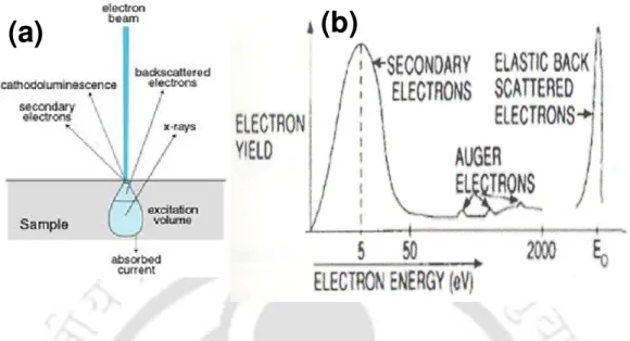
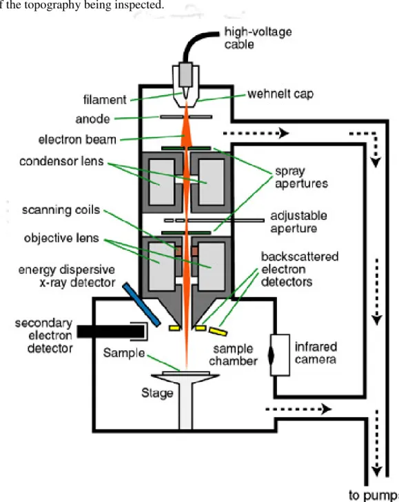
Scanning Electron Microscope (SEM)
These primary bombarding electrons on the surface of the sample remove electrons from the sample. These signals are amplified, analyzed and translated into images of the topography being inspected. By measuring the value of the energy of X-rays released by a sample during electron beam bombardment, the identity of the atoms present in the sample can be established.
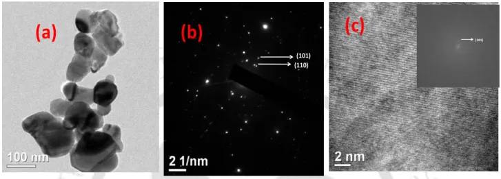
Transmission Electron Microscope (TEM)
This is done by placing appropriately sized apertures in the back focal plane of the objective lens. Here, we could do the exact centering of the diffraction ring and by choosing the right distance on the nm-1 scale, the exact value of the dhkl plane in real space could be determined. We first perform the fast Fourier transform of the HRTEM image which converts the real space crystal planes into imaginary spots in k-space, from this we may be able to determine the distinct plane dhkl.
FTIR and Raman Spectroscopy
- FTIR Spectrometer
- Raman Spectrometer
Half of the beam was reflected to a stationary mirror and returned to the splitter, while the other half was reflected back by a movable mirror. The position of the moving mirror is measured using a laser, as shown in Figure 2.8 (b). Furthermore, the beam was allowed to enter a charge coupling device, where it detects the change in polarizability of the sample due to the change in wavelength and converts it into the intensity.
Vibrating Sample Magnetometer
The temperature variation up to 20 K was obtained using an OXFORD make CCR cryostat (model X together with the temperature controller. Calibration of the vibrating sample magnetometer was done by measuring the magnetic moment of a standard pure Ni sample. The VSM is based on Faraday's law, according to which an emf is induced in a conductor by a time-varying magnetic flux.
Electron Spin Resonance
The microwave can be amplified by the Klystron and is allowed to move in one direction with the help of an isolator. Furthermore, the power of the microwave can be reduced with the help of the attenuator. The cavity is placed between the pole pieces of an electromagnet, and the magnetic field can be swept.
Electrical Resistivity Measurements
To summarize, I used various experimental facilities such as X-ray diffractometer, scanning electron microscope, transmission electron microscope, FTIR spectrometer, Raman spectrometer and ESR setup to characterize the samples. The electrical resistance as a function of temperature was measured using linear two probe technique with the help of SourceMeter unit.
Co doped SnO 2 based DMS
- Preparation and Characterization
- Magnetic Properties
- ESR Analysis
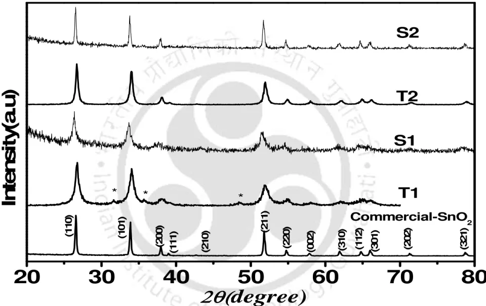
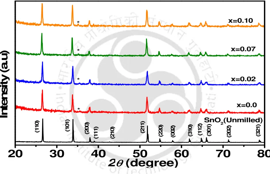
The lattice parameters are found to decrease marginally with increase in dopant concentration and can be understood in terms of Co2+ or Co3+ replacing Sn4+ ions. The expanded view of (110) peaks is shown in Figure 3.3, where one can see the shift in the peak position towards a higher 2θ value with an increase in doping concentration. For a given doping concentration, the M0 values are found to decrease with increase in temperature and this can be understood as a result of the decrease in ferromagnetic interaction with increase in temperature.
- Preparation and Characterization
- Magnetic Properties
- Electrical Resistivity Measurement
Compared to our solid state route prepared Co-doped SnO2, where the crystallite size was of the order of 60 nm as given in table-3.1, here the highest crystallite size was found to be 15 nm. The electrical resistance of air-annealed samples at room temperature is found to be in the order of 109 Ω-cm, and their temperature variation could not be measured due to large resistance beyond the measurement limit of the instrument used. On the other hand, the electrical resistance of nitrogen-annealed samples is found to be about two orders of magnitude smaller than that of the air-annealed material.
Ball Milled Pure SnO 2
- Sample Preparation and Characterization
- Magnetic Properties
- ESR Measurement
The observed peak at 475 cm-1 for samples T1 and S1 corresponds to the Eg mode of vibration. The observed ESR signal in T1 and S1 may be due to the polarized electron spin at the oxygen vacancy. Due to the presence of a large molecular field, the resonance occurs at a low applied field.
Co doped SnO 2 by Ball Milling
- Preparation and Characterization
- Magnetic Properties
The lattice parameters of spinel structural phase are found to be about 8.40 Å, and are comparable to the reported value of ferrites [263]. This can be understood in terms of Fe contamination due to the ball milling process using the steel vial. In contrast to x = 0 sample, no secondary transition is observed, and this may be mainly due to the strong FM signal of Co-doped samples.
Critical Behavior Studies
The values of the critical exponents β, γ and δ determined from the above analysis are given in Table 3.15. This suggests that the values of critical exponents and TC determined by analysis are quite accurate. It is also found that the experimental values of these critical exponents are quite close to the mean-field model.
Summary
It was found that the critical exponents obtained are comparable to the values predicted by the mean field model, i.e. We also estimated the critical exponent, γ, based on the Kouvel-Fisher method and found it to be consistent with the result of the MAP method. It was found that the temperature variation characteristic of the effective critical exponent γeff is comparable to the theoretical prediction of a disordered system.
Ni-doped SnO 2 Series
Ni-doped SnO 2 by solid state route
- Preparation and Characterization
- Magnetic Properties
- Resistivity Analysis
- ESR Measurement
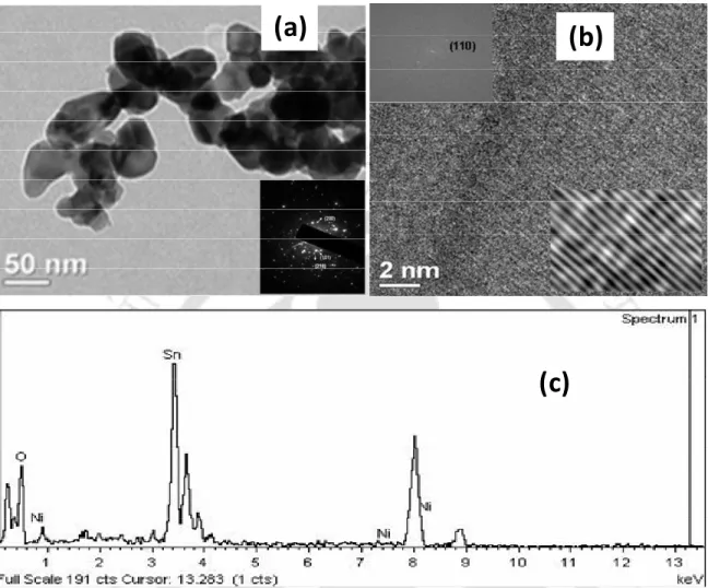
The cation ratio obtained by EDX analysis is given in Table 4.2 and is found to be comparable to the nominal initial composition. The mean radius of the BMP was estimated from the fitted value of meff and assuming a spherical shape of the BMP, and was found to be 60 Å for the x = 0.07 sample at 80 K. The values of meff were found to increase with temperature and this may be mainly due to the change in BMP size.
Ni-doped SnO 2 by ball milling
- Preparation and Characterization
- Magnetic Properties
- ESR Spectra
Summary