I also want to thank the coordinators of the National Program on Smart Materials Project, Dr.
Introduction
Silicon Integrated Passive Devices
Capacitors such as metal oxide semiconductor (MOS), i.e. polysilicon-gated capacitors on single-crystal silicon, metal insulator metal (MIM) and metal oxide metal (MOM) are offered in silicon technology. Passive devices are selected depending on the specifications related to the application area and the technology adopted for implementation.
On-Chip Inductor
This can be understood by considering the metal segments of the spiral inductor as microstrip transmission lines as shown in Fig 1.5. This electrically induced displacement current flows vertically, perpendicular to the plane of the coil inductor as shown in Fig 1.7.
![Figure 1.2: Planar inductor structures [1].](https://thumb-ap.123doks.com/thumbv2/azpdfnet/10344851.0/26.918.185.756.90.605/figure-planar-inductor-structures.webp)
Review of Si On-Chip Inductor Design and Opti- mizationmization
Spiral Inductor Structures
29] suggested that the series resistance of the inductor could be minimized by increasing the thickness of the metal by shunting multiple metal layers, as shown in Figure 1.8. This configuration of the inductor structure showed that the frequency at which the Q peaks can be changed by selectively shunting metal layers.
![Figure 1.8: Cross sectional view of a spiral inductor showing the shunting of metal layers M2, M3 and M4 in a four metal layer process and the metal underpass in metal layer M1 [3].](https://thumb-ap.123doks.com/thumbv2/azpdfnet/10344851.0/33.918.217.772.84.430/figure-cross-sectional-inductor-showing-shunting-process-underpass.webp)
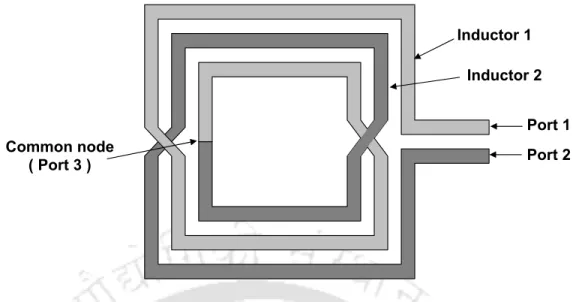
Common node ( Port 3 )
- Quality Factor Enhancement Techniques
- Inductor Design and Optimization Methods
- Motivation and Problem Description
- Organization of the Thesis
- Summary
- Introduction
- Bounding of Layout Parameters
The dependence of the quality factor and the inductance on these parameters has been studied in detail. ASITIC' (Analysis and Simulation of Spiral Inductors and Transformers for ICs) for design, optimization and modeling of spiral inductors and transformers.
Number of turns
Performance Study of Fixed Value Inductors using EM Simulator
- Area of the inductor
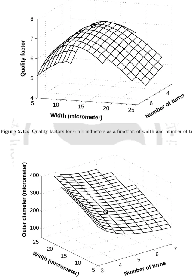
- Quality Factor Variation with the Number of turns
- Quality Factor Variation with the Metal Width
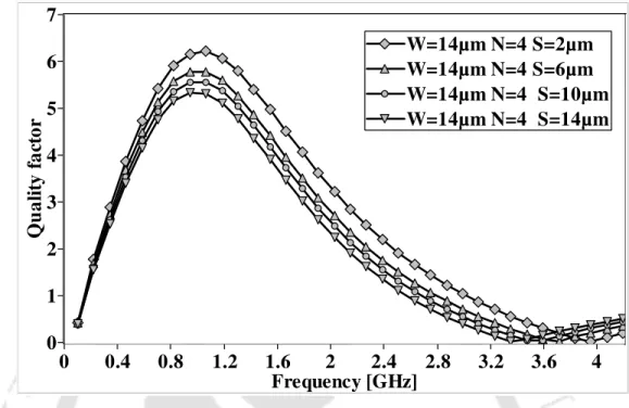
- Quality Factor Variation with the Spacing between the Metal TracksTracks
In other words, for a smaller number of turns since the inner diameter is large, the eddy current effect decreases and the quality factor increases. Thus, spiral inductors designed with a larger number of turns to save area will suffer from a low quality factor. However, further reducing the number of turns from 4 to 3 by increasing the inner diameter does not improve the quality factor, but instead increases the area (Dout × Dout) and the total length.
As the length increases, the series resistance of the coil increases and hence the quality factor decreases. Milling also increases with the number of revolutions when the width is fixed as the surface is reduced.
Efficient Optimization with Bounding of Layout Pa- rameters
- Lumped Element Model of a Planar Spiral Inductor
- Calculation of Figure of Merits
- Performance Evaluation with an Optimization Example
- Computational Speed
- Global Optimal Quality Factor Trade-off Curve
- Peak Quality Factor Variation with Inductance
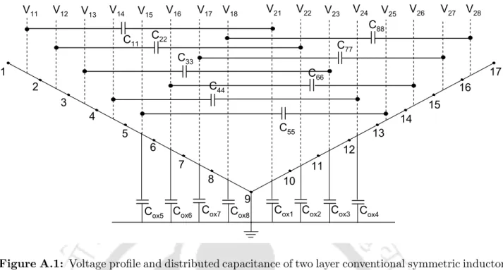
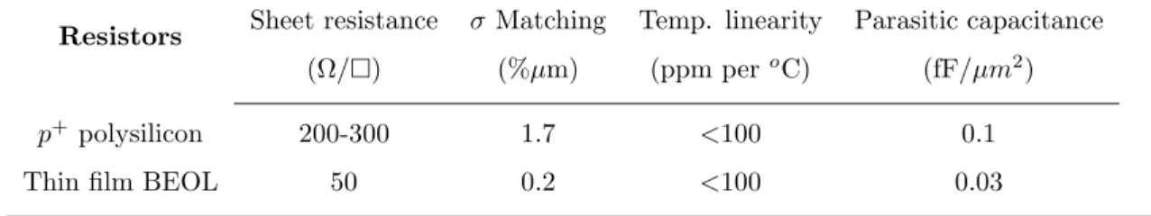
This increases the total length of the spiral and thus increases the parasitic series resistance, as can be seen in Figure 2.13, so the quality factor is highest at minimum spacing. The inductance and resistance of the coil and chassis are represented by the series inductance, Ls, and the series resistance, Rs. CSi and RSi are the capacitance and resistance of the silicon substrate, respectively, and Cox is the oxide capacitance between the coil and the silicon substrate, calculated as .
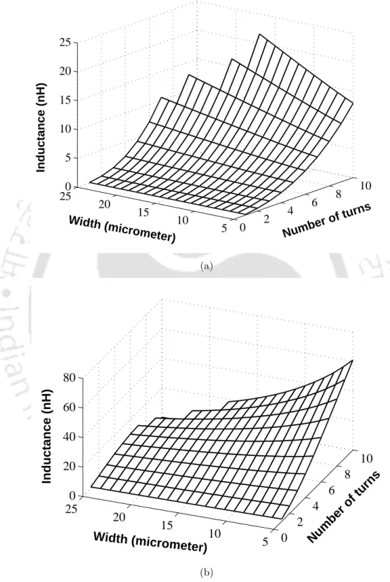
In the summation method, the time required for the optimization or the number of function evaluations will depend on the discretization of the design space (N, W and Dout). The trend of variation of the corresponding optimum width, number of turns and outer diameter is shown in Fig.
Optimization using EM simulator
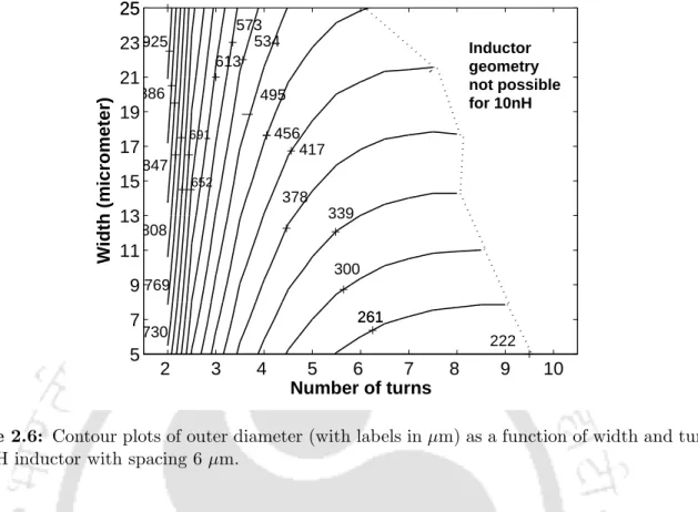
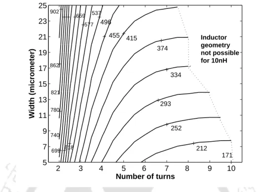
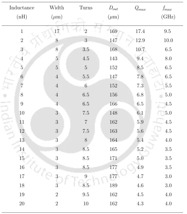
At the desired operating frequency, the width of the structure with the highest quality factor is the optimal width. An investigation into the trade-off between the quality factor and area can also be carried out. We find the optimum 10 nH inductor with quality factor of 5.9 at 1 GHz for the same technology in Table 2.2.
With a 5% decrease in the quality factor, we can choose the inductor with 7 turns as the optimal one, which saves an area of 41.2%. Therefore, for a given technology, the optimal combination of number of turns, width and inner diameter resulting in the highest quality factor at the desired operating frequency can be determined with certainty for each technology.
Summary
Since the feasible region for any desired inductance value is determined a priori, the optimization leads to a global solution and the method is very fast. Since limit curves can be adjusted to include all the desired range of inductance, the method is more advantageous when multiple inductors of different values need to be optimized. Several important fundamental deviations of the design such as quality factor and area, quality factor and inductance, quality factor and operating frequency, maximum quality factor and the peak frequency etc.
With layout-parameter bounding, the enumeration method has been shown to be as fast as other numerical algorithms. Therefore, optimal spiral inductors can be synthesized and analyzed in an easy and simple way in a matter of seconds.
Introduction
Design of the MPS Inductor Structure
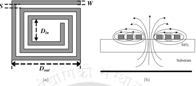
The second pyramidal spiral inductor starts winding from the bottom metal plane, M1 with the outer (first) turn and the second turn on M2 and repeats until it ends with the inner turn on M4. So for each inductor the turns of the metal track run in different metal layers and the inner diameter changes proportionally to avoid the overlapping of the turns and spirals up and down in a pyramidal fashion and hence the name. There will be coupling between these two inductors and the total inductance is given by the sum of its own and mutual inductances.
The jth turn of one inductor overlaps with the same jth turn of the other inductor as seen in Fig. Process technology top metal layers are used to avoid thinner bottom metal layers and associated substrate losses.
Lumped element model of the MPS Inductor Struc- tureture
The jth turn of one inductor overlaps with the same jth turn of the other inductor as shown in fig. 3.2, and winding up and down is achieved by means of two passes between adjacent metal layers. An inductor's self-resonance frequency is defined as the frequency at which the maximum magnetic energy becomes equal to the electrical energy, i.e. the inductive reactance and the capacitive reactance become equal and opposite. The voltage across each turn or segment of the inductor is denoted by Vij, where i is inductor 1 or 2 and j is the turn number 1, 2, 3 or 4 of each inductor.
Aj is the area of the jth turn in terms of outer diameter Dout, metal width W and offset Of f given by. Here, n represents the number of turns of the spiral inductor in each stacked layer and the number of turns of each inductor of the two-layer symmetrical inductor.

Characterization of the MPS Inductor Structure
- Performance trend of MPS inductors
- Comparison of MPS with its equivalent planar inductor struc- turestures
- Comparison of MPS with multilayer conventional symmetric and asymmetric stack structuresand asymmetric stack structures
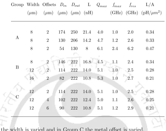
The inductance, peak quality factor and self-resonance frequency are also given in Table 3.1. The change in diameter in Group A results in a significant change in inductance and quality factor in contrast to the change in width and metal displacement. In group C, as the metal offset increases, the inductance decreases while the quality factor is almost constant.
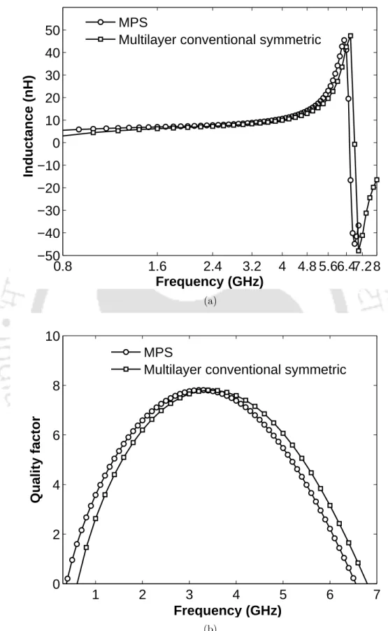
The effect of changing the process parameters on the inductance, quality factor and self-resonance frequency of the MPS inductors was also studied. At low frequency, the quality factor of the MPS inductor and the conventional symmetrical inductor are almost the same, but higher than the planar asymmetrical pair.
Experimental Verification
- Process Parameters
- Layout of MPS Inductors
- Deembedding Process
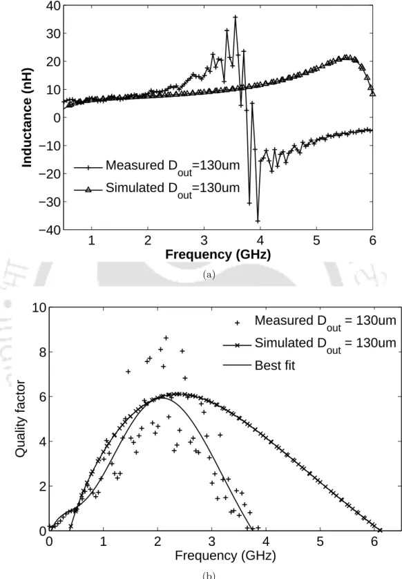
- Measured Results and Discussion
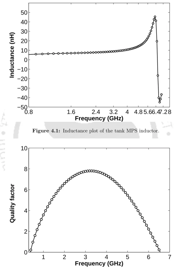
To evaluate the performance of the MPS inductors, we fabricated some MPS inductors and the layout parameters are given in Table 3.7. The 130 µm outer diameter inductor will be used in the tank of the VCO, which will be discussed in the next chapter. For accurate characterization on the device wafer, the deembedding process should be performed, subtracting the parasites due to the probe pads and the metal compounds from the measurement of the device under test (DUT), i.e. inductors in this case.
The embedding is therefore done in two steps, as shown below. i) The S parameters of the DUT in a luminaire are measured. The S parameters of the single short armature are measured and displayed by Senkele short armature.
Summary
To estimate the equivalent parasitic capacitance and self-resonant frequency, a compact model with a closed-form expression was also developed. The performance of MPS inductor was also compared with other reported symmetrical inductors in literature. With multilayer pyramidal symmetrical inductor, the area occupied by the inductor in integrated circuits will be significantly reduced and the cost will be minimized as a result.
The proposed four-layer structures with an outer diameter of 130 µm resulted in an inductance of 6.9 nH at 1 GHz with a peak quality factor of 6 at 2.1 GHz, while the inductor with an outer diameter of 222 µm has an inductance of 27 nH at 1 GHz with a peak quality factor of 3 at 1.1 GHz.
Introduction
Passive elements of the LC tank
- Inductor Design
- Varactor Design
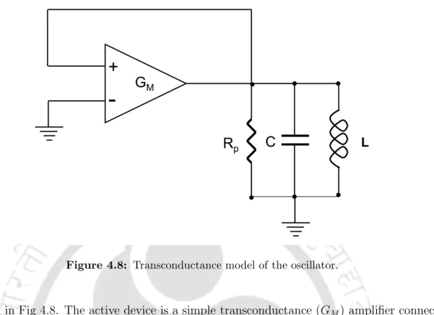
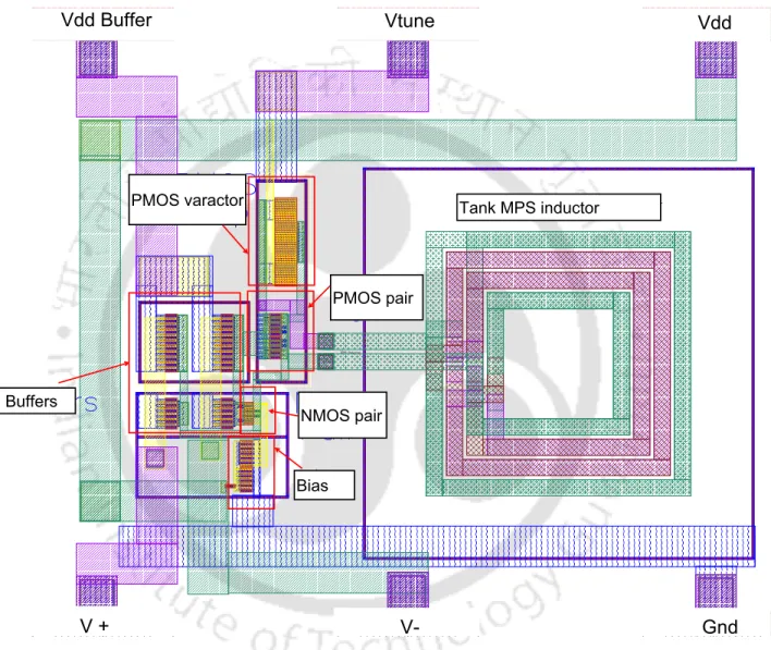
To minimize the area, the inductor of the LC tank is implemented with the new multilayer pyramidal symmetric inductor structure. The total capacitor of the LC tank includes the combination of the tank capacitor connected across the inductor, the NMOS and PMOS parasitic capacitances and the inductor's parasitic capacitance. The oscillator frequency will be set by changing the capacitance of the tank with a controlled voltage.
Due to the parasites, the width of the PMOS capacitor has been adjusted so that the circuit oscillates at 2.4 GHz. The variation of the total tank capacity with the control voltage connected to drain and source of each tank capacitor is shown in Fig 4.5.
VCO Circuit Design
According to Barkhausen's criteria for circuit oscillation, this negative resistance will exactly cancel out the equivalent parallel resistance of the tank circuit. In other words, the active device must add enough power to the circuit to cancel out the total tank circuit losses. This condition determines the minimum size of PMOS and NMOS transistors.
This tail current device can change the voltage swing across the tank circuit of the oscillator. The negative resistance seen across the tank circuit can be changed by changing this current and therefore the actual equivalent parallel resistance (Rp) of the resonator can be determined experimentally by finding the lowest bias current at which the circuit will oscillate.
VCO Simulation
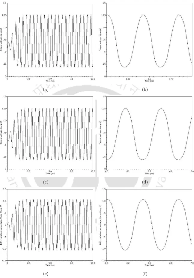
All the parasitic capacitance due to the bond pads, the parasitic bond wire inductance and the electrostatic discharge protection circuits are included in the simulation.
Measurement Results and Discussion
It can be noted that if the differential output were to be measured, the phase noise would be reduced by 6dBc as the oscillation amplitude would nearly double. The performance of the VCO with the new multilayer inductor can be compared to other oscillators based on the commonly used figure of merit (FOM) [94].
Summary
Conclusions
The performance trend of MPS inductors was demonstrated by varying their width, outer diameter and metal offsets. Two structures with an outer diameter of 130 µm and 222 µm and a width of 8 µm were fabricated in UMC 0.18 µm RFCMOS process and characterized on wafer. The proposed four-layer structures with an outer diameter of 130 µm resulted in an inductance of 6.9 nH at 1 GHz with a peak quality factor of 6 at 2.1 GHz, while the inductor with an outer diameter of 222 µm has an inductance of 27 nH at 1 GHz with a peak quality factor of 3 at 1.1 GHz.
The multilayer pyramidal symmetric inductor is implemented in the LC tank of a 2.4 GHz voltage controlled oscillator. The performance of the VCO meets the specifications for various applications in the 2.4 GHz to 2.5 GHz unlicensed ISM band and with the new inductor it will be beneficial with a large reduction in the chip area.
Directions for Future Research
Papananos, "Systematic Analysis and Modeling of Integrated Inductors and Transformers in RFIC Design," IEEE Trans. Bausells, “Improving the quality factor of RF integrated inductors through layout optimization,” IEEE Trans. Yeh, “Design and Fabrication of High Q Suspended Spiral Inductors Compatible with Deep Submicron CMOS Technology,” IEEE Trans.
Patra, “ANN and PSO-based synthesis of on-chip spiral inductors for RF ICs,” IEEE Trans. Do, “Physical Layout Design Optimization of Integrated Spiral Inductors for Silicon-Based RFIC,” IEEE Trans.