This is to prove that the thesis titled "Micro-Scale Power Management Interface Circuits for IoT Node" submitted by me to the Indian Institute of Technology Guwahati for the award of Doctor of Philosophy degree, a genuine work of carried out by me under the supervision of Prof.
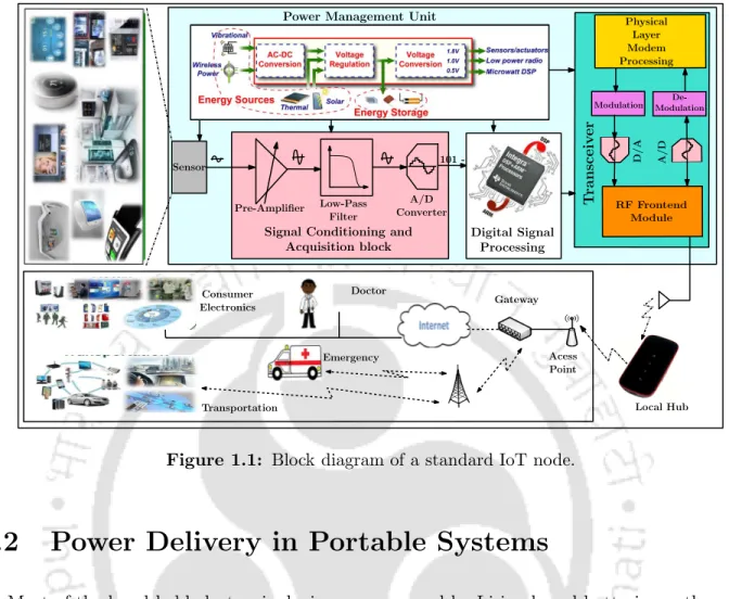
Introduction
Power Delivery in Portable Systems
To protect the battery from undervoltage (UV) and overtemperature (OT), a battery management unit is required. Since the battery is the only energy source, the system can be shut down when there are no load requirements.
Power Delivery in Self-Powered Systems
Scavenging Light Energy
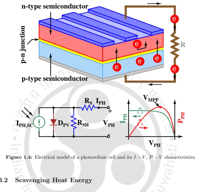
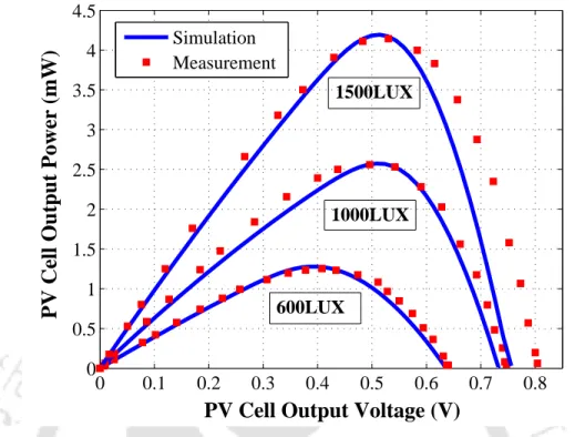
But in reality, there is some non-zero series resistance and final shunt resistance, which reduces the conversion efficiency of the solar cell. From the power-voltage characteristics of the PV cell, it is clear that the amount of extractable power depends on the cell voltage, VP H, and one can extract the maximum power by setting the PV cell voltage to the maximum power point (MPP) voltage, i.e. VP H =VM P P.
V MPP
V PHVPH
R SHD PV
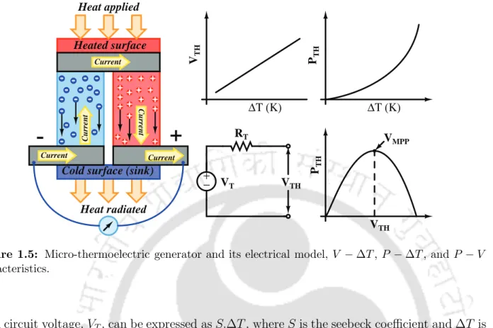
Scavenging Heat Energy
The variation of the output voltage, VT H , and the output power, PT H , with respect to ∆T and the variation of the output power with respect to the open-circuit voltage are also shown in Figure 1.5. Since the internal resistance is modeled by a resistor, a one-time resistance matching circuit is required to extract maximum power from the thermoelectric harvester.
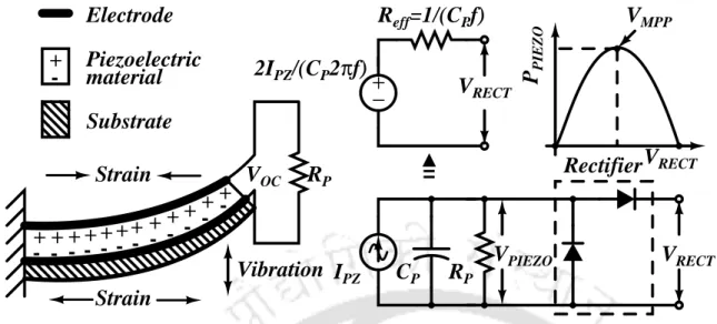
Scavenging Vibrational Energy
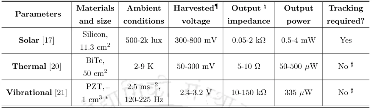
Even in the presence of diode non-idealities, voltage doubler usually provides higher output power compared to a full-bridge rectifier [19]. Therefore, systems giving typical power density in microwatts would be useful for portable applications, and typical power density of several milliwatts would be suitable for industrial applications.
Energy Storage Options for Portable Systems
- Why Do We Need a Storage Unit?
The typical input-output power characteristics of the sensor nodes and their differences are shown in Fig. 1.8. The curve in red indicates the power consumption of the sensor node for processing and transmitting the recorded data.
P OUT
P INPIN-POUT
- Conventional Batteries
- Thin Film Batteries
- Supercapacitor
- Motivation for this Work
- Problem Definition
- Thesis Contributions and Chapter Organization
- Introduction
- Linear Regulators
Moreover, the energy processing paths must be stable with respect to the source and load variations [5]. In order to get many independent power sources from a single energy source, regulators are essential to match scaled voltages to the respective loads.
Start-up
Feedback network
Current sense
LDO Regulator
Since, the pole ωP1 depends on the gain of the pass transistor AP, its frequency will change approximately by. On the contrary, the output impedance and gain will increase by reducing the load current, but the pole frequencies decrease and the phase difference degrades as the non-dominant pole moves close to the GBW. The slew rate of an LDO essentially depends on the gate capacitance of the pass transistor and the bias current of the error amplifier.
V OUTVREF
C LIL
Dominant Pole
Loop
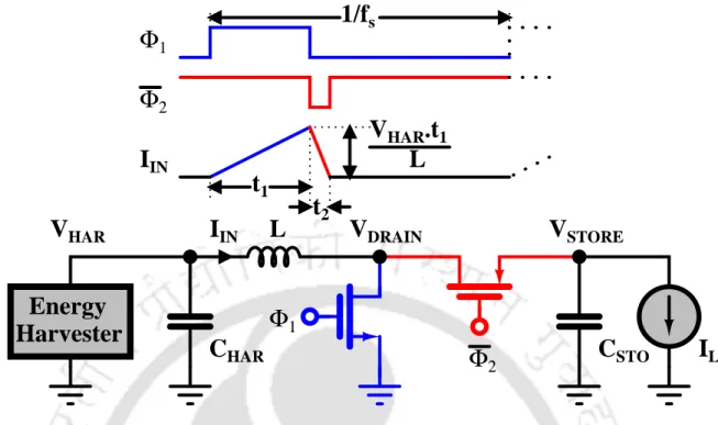
Inductor Based DC-DC Converter
Energy Harvester
C STOCHAR
V STORE
I LVHARIIN
Low-Side switch
High-Side switch
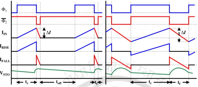
Discontinuous conduction mode boost converter
The output phase relationship of discontinuous conduction mode power is quite different from that of continuous conduction mode power phase. During the first switching phase Φ1, the inductor current increases to VHAR×t1/Ground during the second switching phase Φ2, the inductor current ramps.
V STOREL
Φ 2VDRAIN
I LVHAR
V HAR .t 1 L
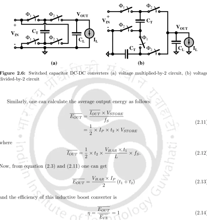
Switched Capacitor Based DC-DC Converter
Switched capacitor based DC-DC converter transfers energy by periodic charging and discharging of capacitors from the supply to the load. During the positive phase of Φ1, CT is connected to the power supply and is charged to VIN, while the load capacitor CL is connected to the load and discharged by the current load IL. Thus, in steady state one can expect twice the input voltage minus the loss due to the current through load, as given by. 2.15) where TS represents the duration of the clock cycle.
Summary and Conclusions
Ideally, an inductive boost converter will provide 100% efficiency, while a capacitive converter will only provide 100% efficiency at one point when the output voltage is equal to the open-circuit voltage of this topology. However, current manufacturing processes do not allow integration of high-performance inductors for power management applications, and thus conversion efficiency decreases linearly with technology node. However, they suffer from poor conversion efficiency as the load voltage moves further away from the open-circuit voltage, and one can mitigate this problem by including converters with multiple gain settings and by choosing one whose open-circuit voltage is closer to the desired load voltage . .
Introduction
Literature Survey
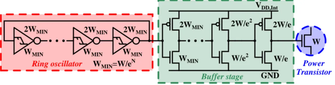
CTS) to eliminate the charge transfer loss due to VT H-drop as shown in Fig. 47] proposed a tree topology QP similar to Ming QP, to meet the minimum supply voltage constraints as shown in Fig. 48 shown to mitigate] replace the non-overlapping clock signals with a single-phase charge pump as in Fig.
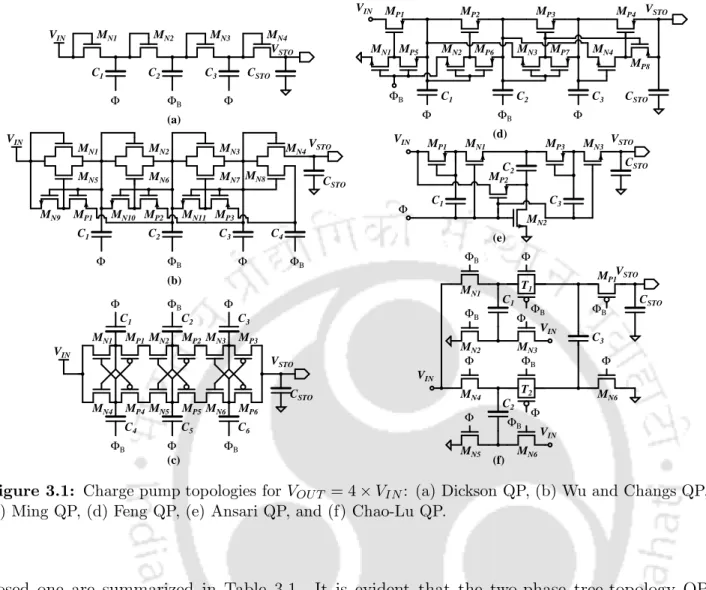
Proposed Tree-Topology Charge Pump Circuit
The maximum output voltage that can be achieved for a number N of phases can be estimated as. 3.1) and the average output current will be. Since the number of stages plays a critical role to maximize the net harvested power and minimize the silicon area, the optimal number of stages can be expressed using the analysis presented in [49] or [50], that is. 3.3) With the help of the optimal number of phases, the required value of C for a single-phase QP tree topology is obtained.
Power Transfer Loss from a System Level Perspec- tive
- Conduction power loss
- Switching power loss
To achieve higher efficiency, these interface circuit power losses must be minimized. PSW B, LOSS ≈NCOX(W L)nVDD,Int2 fclk. 3.7) Switching power loss due to ring oscillator is. Since the width of the transistor is directly proportional to the switching loss and inversely proportional to the conduction loss, an optimal width of the transistor must be found such that the power transfer loss is minimal.
Measurement and Simulation Results
- Photovoltaic harvester
- Tree-topology single-clock charge pump
Therefore, the optimal power transfer loss of a power harvesting interface circuit is obtained at PLOSS,OP =PBIAS,LOSS+ (NN + 2NP)IONVDD,IntLn. The power transfer loss and the optimal width of the power transistor increase as the VDS drop increases. The output power of the proposed QP circuit with different input voltages is much higher than the chow-Lu QP circuit, since the power transfer loss is minimal.
Summary and Conclusions
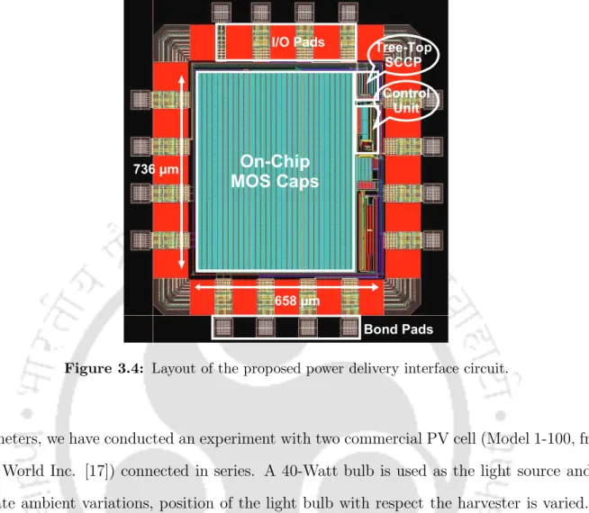
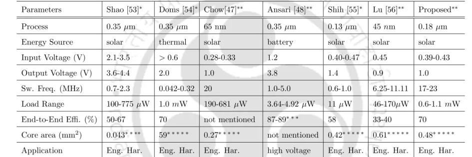
On-chip measured results;∗∗Postlayout simulation results;∗∗∗Power transfer losses are not considered;∗∗∗∗without pump capacitors; ∗∗∗∗∗with pump capacitors; Scary.
Introduction
Literature Survey
Therefore, this type of scheme is also a one-time design and implementation scheme for a specific PV cell and not an adaptive scheme. In this method, a variable disturbance is given in the operating ratio of a power inverter, which will disturb the current of the PV cell and effectively change the operating voltage in the PV cell. Moreover, this scheme requires power-hungry current/voltage sensors, analog and digital comparators, flip-flops, microcontrollers, etc.
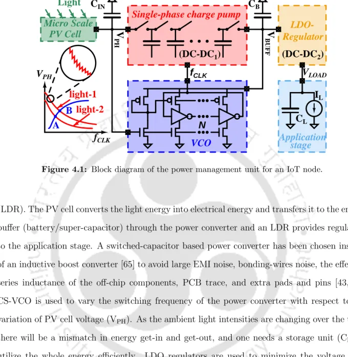
Overall Energy Harvesting System
The PV cell converts the light energy into electrical energy and transfers it to the energy buffer (battery/super capacitor) through the current converter and an LDR provides regulation to the application stage. The CS-VCO is used to vary the switching frequency of the power inverter with respect to the variation of the PV cell voltage (VPH). When the input impedance of the power converter is matched to the impedance of the harvester, maximum power transfer will occur from the harvester to the interface circuit.
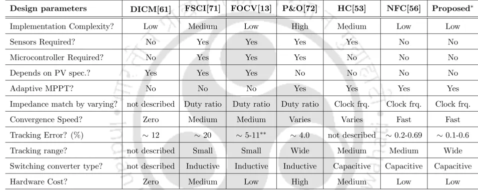
MPPT Schemes Suitable for IoT Applications
No No No Yes Yes Yes Yes. not described Duty ratio Duty ratio Duty ratio Clock frq. Zero Average Average Varies Varies Fast Fast. not described Small Small Wide Medium Medium Wide. not described Inductive Inductive Inductive Capacitive Capacitive Capacitive.
Switching freq. (f CLK) PV cell output voltage (V PH )
A Blight-1
V MPP2
V MPP1
Equation (4.5) Equation (4.6)
Analytical Modeling for Proposed MPPT Scheme
The effect of load condition can be visualized by writing an expression for VBU F F from equation (4.1) by replacing IOU T with IL as given in equation (4.2). When the PV cell is connected to this charge pump, the input current and voltage will be the output current (IPH) and voltage (VPH) of the PV cell. The maximum power transfer occurs when the input impedance of the power converter matches the PV cell impedances.
MPP V PH
Measurement and Simulation Results
- Photovoltaic harvester, CS-VCO, and power converter
- MPPT Transients
- CL-LDO voltage regulator
- Complete system simulation
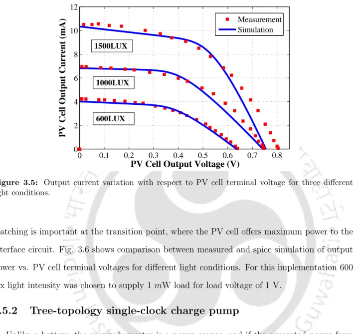
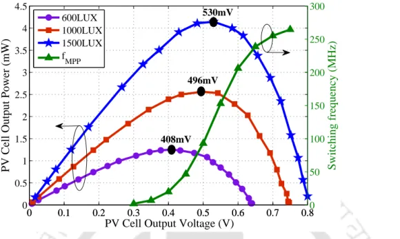
The variation of the output power with respect to the connection voltage of the PV cell for three different lighting conditions (600 lux, 1000 lux and 1500 lux) is shown in figure. Initially, the PV cell provides maximum output voltage with minimum output current to the CS-VCO and power converter circuits. To emulate the light irradiation, the photocurrent, IPH, is varied from 3.30 mA to 4.01 mA and the corresponding variation of the PV cell terminal voltage, switching frequency, buffer voltage and load voltages are shown in Fig.
Summary and Conclusions
Tracking speed not described not described not described not described ~30 s ~4.5-7.0 µs ~12 µs MPPT overhead MCU, PS, Comp. PS: photosensors; CS: current sensor; ZCD: Zero Current Detector; Comp.: Comparator; SC: supercapacitor; IBC: Inductive Boost Converter; CBC: capacitive boost converter; PV-PC: PV pilot cell; TG: Portable door; P-VCO: polynomial VCO; tCH: inductor charging time; tDCH: inductor discharge time;♠: nF capacitor was chosen to reduce simulation time;¶: consider MCU and PS;.
Introduction
Traditional Power Management Architecture
A cold start block is incorporated to bring the system from the sleep state to an active state when the harvest output voltage is lower than the threshold voltage of the MOSFET. Therefore, improving the efficiency of one of these two converters will improve the efficiency of the system and conversely, it will degrade the efficiency of the system. Extensive research has been conducted and a number of articles have been reported on switching regulators and LDO regulators (LDR) [9, 78] for power management applications.
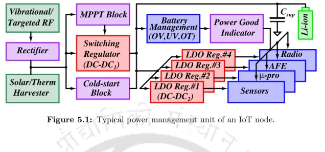
Proposed Architecture
The proposed architecture uses a single DC-DC converter to maintain regulation at the input and output. To provide regulated power when there is enough ambient energy to power the load, a reduced version of the load voltage is compared to internal reference voltages, VR1 and VR2. Conversely, if there is not enough environmental energy to supply the load, ie. VL < VR2, the control signals will couple the charge pump and buffer stage (inverter mode) to the application stage to maintain load regulation.
Circuit Implementation
During the positive half cycle of clock Φ, capacitor C2 will be charged from the stripper and capacitor C1 will be discharged to the capacitor C3. To generate these control signals, Comp1 compares VDIV with VREF1 and activates either VM8 or VM9 during the negative half cycle of Φ, and their corresponding timing diagrams are shown in Figs. showed. If VDIV is lower than VREF1 during the negative half cycle of Φ , VM8 will activate the M8 transistor and VM9 will turn off both M9 and M11 transistors to maintain load regulation.
Start-up mechanism of the Proposed Power Man- agement Unit
When the load voltage reaches the trigger voltage of the detector (D1), the control signal S1 changes its state and disconnects the start-up charge pump from the load capacitor and the ring oscillator, establishing two connections: one, between the ring oscillator and the DC-DC converter, and another between the load capacitor and the ring oscillator. This is the warm-up mode where the DC-DC converter charges the load capacitor. When the DC-DC converter begins to transfer charges from the harvester to the load capacitor, the load voltage increases, which will trigger the D2 detector to make connections to supply the load circuit and to start the controller.
Measurement and simulation results
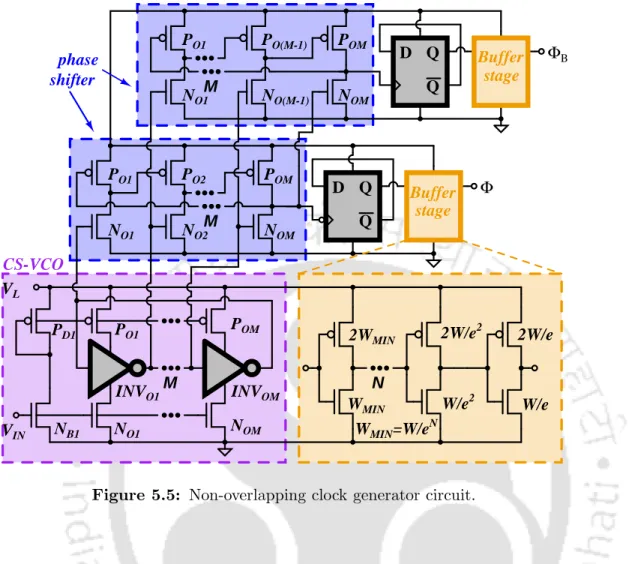
- Non-overlapping clock generator
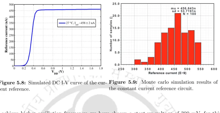
- CMOS current reference circuit
- Voltage detector
- Tree-topology charge pump circuit
- Complete System Simulation
It should be noted that the input impedance of the power converter depends on its switching frequency, and thus one must choose a switching frequency so that the harvester can transmit maximum power to the harvester. Therefore, an appropriate triggering of the control signals takes place to provide better load regulation. Once the interface circuit provides regulation at the load, the overall efficiency of the system is calculated.
PMUDMM
PVLM
- Experiment results
- Summary and Conclusions
- Conclusions
- Summary of Contributions
- Future Directions
Otis, "An inductorless dc-dc converter for energy harvesting with a 1.2-µW bandgap reference output controller," IEEE Transactions on Circuits and Systems II: Express Briefs, vol. Paily, "An efficient on-chip switched-capacitor -based power converter for microscale energy transducer,” IEEE T. Venchi, “An interface circuit for low-voltage-low-current energy harvesting systems,” IEEE Transactions on Power Electronics , vol.