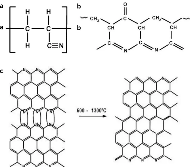
In particular, nitrogen-doped graphene (N-doped graphene) is expected for industrial use due to the widening of the graphene band gap and the potential to offer a catalytic site for oxygen reduction reaction, ultracapacitor, etc. Polyacrylonitrile (PAN), which is a well-known precursor of carbon fiber, is a suitable material for the commercialization of N-doped graphene because it is already produced by many companies. The stabilization process is an important factor to consider in order to obtain continuous N-doped graphene films.
An atomic force microscope and a scanning electron microscope confirmed that N-doped graphene forms a continuous, single-layer film. The stabilized PAN structure.3 (c) Structure changes for PAN precursor during carbonization.4.. a) Experimental process of conversion of PAN to N-doped graphene using CVD. The spectrum of the blue line is the N-doped graphene. a) XPS spectrum of the N-doped graphene on SiO2 (300 nm)/Si substrate.
The inset image shows the XPS N1s spectrum of the cleaned SiO2/Si substrate. a) XPS N 1s spectra of N-doped graphene with temperature. configuration of graphene nitrogen with temp. Optical image of different concentrations of PAN after the same conversion conditions without Pt but Cu. Raman spectra of PAN after the same conversion conditions using Cu. a) Schematic of an N-doped graphene FET device.
Introduction: Research background for the conversion of polyacrylonitrile to N-doped graphene Graphene is a single-layer carbon film with honeycomb lattices.
Introduction: Research background for conversion of polyacrylonitrile to N-doped graphene
- Properties of graphene
- Properties of N-doped graphene
- Synthesis methods of graphene
- Synthesis of graphene using polymers as precursor
- Synthesis of N-doped graphene
- Future of graphene
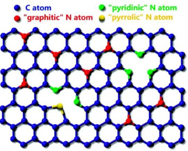
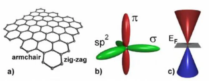
Graphene is considered a promising material to replace silicon due to its outstanding electronic properties. It is difficult to use in industry due to the absence of the band gap essential for semiconductor switching in pristine graphene. As a result, doped graphene shows a change in its electronic structure, widening its band gap.14 There are three substitution sites when a nitrogen atom is doped into graphene (Figure 2).15 The first is the pyridine N, which is located at defects or edges in graphene.
When nitrogen atoms replace carbon atoms in graphene lattice, the nitrogen atoms prefer pyrrolic-N or pyridinic-N sites due to stable thermal energy.16. There are four main methods to obtain graphene, namely, mechanical exfoliation method,5 chemical vapor deposition (CVD) using gas or solid precursors on catalyst substrates,17-18 reduction of graphene oxide,19 and epitaxial graphene growth using SiC -substrates.20 It is well known that graphene synthesis method affects graphene quality and scale. For example, mechanical filling methods produce high-quality graphene, but this technique has limitations in growing large areas and large amounts of graphene.
Graphene growth using CVD is used in many laboratories and is a popular growth method for obtaining graphene. The choice of polymers as graphene precursors is an option towards the commercialization of graphene. Furthermore, polymers are suitable for graphene industrialization because they are easily coated on substrates, such as by spin-coating and the Langmuir-Blodgett method.
Recently, many scientists have reported N-doped graphene growth and its application.29-32 There are two main methods for the synthesis of doped graphene: the first is growth in CVD method, and the second is post-synthesis treatment. Luo, Z group showed that the nitrogen content of graphene can be modulated by nitrogen/methane flow rate.33 However, this method is dangerous due to the use of ammonia, which is dangerous for humans. In addition, Panchokarla's group reported the synthesis of boron- and nitrogen-doped graphene by an arc discharge method.34 However, the arc discharge method has the possibility of damaging graphene.
Graphene is one of the promising materials that will revolutionize industries tremendously due to its excellent properties. Due to its excellent flexibility, it can also be used for flexible electronics.37 In addition, it can be used in fuel cells. For example, N-doped graphene could be used to increase the performance of lithium-ion batteries due to its high surface area, flexibility and high electrical electronic properties.
The Wang group reported N-doped graphene containing 2% nitrogen that showed reversible capacity of 900 mAh/g with a current density of 42 mA.39 Furthermore, Reddy et al. Moreover, N-doped graphene usually exhibits a high spin density. suggested a two- and four-way ORR mechanism in N-doped graphene.41-42 Recently, N-doped graphene reached over 20%. diffusion-limited current density compared to the Pt/C electrode.32 Shao et al. demonstrated high nitrogen-doped stability during ORR compared to commercial Pt.36. Furthermore, N-doped graphene can be used as photocatalysts,43 ultracapacitors29, etc.
Conversion of polyacrylonitrile to N-doped graphene
Experimental section
- Conversion of polyacrylonitrile to N-doped graphene using CVD
- Transfer method
- FET fabrication
- Characterization
For cleaning, the SiO2 (300 nm)/Si substrate was sonicated in an acetone solution for 5 minutes and in an isopropyl alcohol solution for 5 minutes. The sample was used as the cathode and the pure Pt foil as the anode. After the PMMA/graphene was exfoliated from the Pt foil, the sample was cleaned 2 times with deionized water to remove the NaOH.
After that, the sample was air-dried and then immersed in an acetone solution to remove the PMMA. Au (55 nm)/(Ti 5 nm) was deposited on the source-drain pattern using an E-beam evaporator. The manufactured sample was heated at 300 °C for 1 hour to achieve good contact and remove polymer residues.
The electrical properties of the samples were characterized using a four-tip probe station (4200-SCS, KEITHLEY). b) Stabilized PAN structure.3 (c) Changes in PAN precursor structure during carbonization.4.
Result and discussion
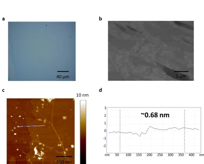
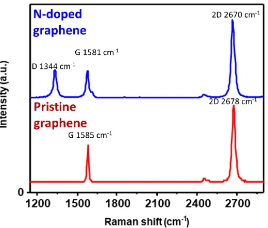
The AFM image shows that the thickness of the N-doped graphene is approx. 0.68 nm, suggesting that it consists of a monolayer film (Figure 7c, 7d). In the Raman spectra, the D band is one of the evidences that nitrogen is doped to graphene because nitrogen causes vacancies and bond disorder in the graphene lattice. The intensity ratio of the G band to the 2D band (I2D/IG) and the 2D band full width at half maximum (FWHM) are used to determine the graphene layers.
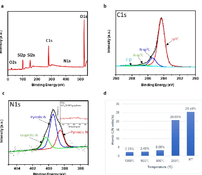
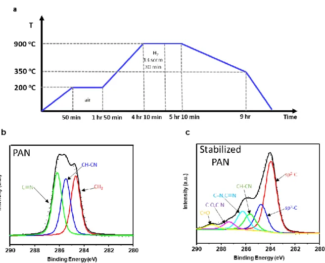
To investigate the bonding configurations of N-doped graphene and the N/C atomic ratio, the samples were examined by XPS. It is also clear that nitrogen is incorporated into the sample compared to N-doped graphene and clean SiO2/Si substrates (inset of Figure 9c, 9c). The main peak, located at 284.2 eV, is assigned to graphitic sp2 carbon.
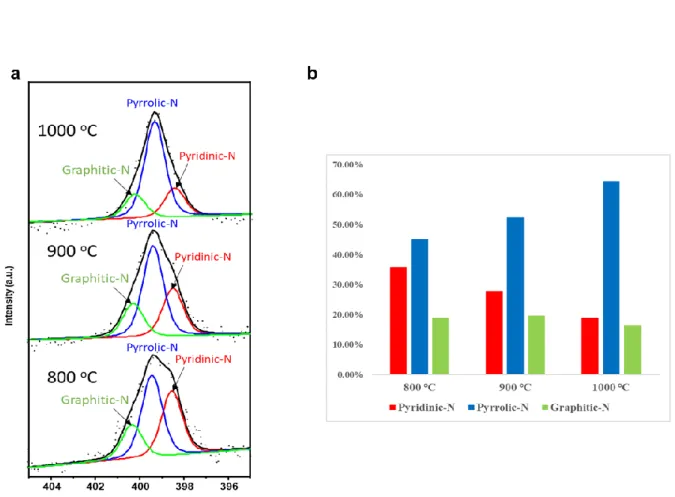
This can be attributed to physisorbed oxygen on N-doped graphene or the incompleteness of deoxidation during the carbonization process. In our spectra, the intensities of pyridinic-N and pyrrolic-N are greater than the intensity of graphitic-N. The result agrees with previous theoretical prediction, which is that nitrogen atoms are more stable at the edges of graphene lattice than at the centers of graphene lattice.16 Figure 9d shows the changes in the ratio of carbon to nitrogen with the conversion temperature. The inset image displays XPS N1s spectrum of cleaned SiO2/Si substrate. a) XPS N 1s spectra of N-doped graphene with temperature.
Red and blue lines were used as 0.5 and 5% PAN solution. a) Schematic of the N-doped graphene FET device. The denitrogenation takes place at the pyridinic N sites during the formation of HCN and NH3.47 The ratio of pyrrolic N and temperature are proportional to each other, which is similar to the relationship obtained in the previous report.56-57. To investigate whether other graphene catalysts could convert PAN to N-doped graphene under our conditions, we attempted to convert PAN to N-doped graphene using copper with the same experimental process.
The reasons why PAN is not successfully converted to N-doped graphene may be due to oxygen in polymers as air changes copper to copper oxide, which has a rare catalytic effect to form graphene, or because copper has a weaker graphitization ability compared to Pt.58 -59. We fabricated the bottom gate effect transistors (FETs) from N-doped graphene to identify electrical properties of nitrogen doping effects. The result indicates ohmic contact forming between the N-doped graphene and the Au/Ti pads, which act as a source and drain.
The figure shows that the Ids decrease as the Vg decreases, which is consistent with n-type behavior. 𝑊𝐶𝑜𝑥𝑉𝑑𝑠 (1) where L and W denote the channel length and channel width, respectively, and Cox is the capacitance per unit area of the gate insulator, which is SiO2 (300 nm) in the sample.
Conclusion
B.; Maiyalagan, T.; Wang, X., Review of recent advances in nitrogen-doped graphene: synthesis, characterization and its potential applications. Cho, K., Heterogeneous solid carbon source-assisted growth of high-quality graphene via CVD at low temperatures. ONE.; Tanemura, M., Field emission characteristics of pristine and N-doped graphene measured by in-situ transmission electron microscopy.
C.; Chen, P.; Wang, X., Electrodeposition of Pt on three-dimensionally interconnected graphene as a free-standing electrode for fuel cell application. Guigon, M.; Oberlin, A., Heat Treatment of Pan-Based High Tensile Carbon Fibers - Microtexture, Structure and Mechanical Properties. Kaburagi, Y.; Hishiyama, Y., Highly crystallized graphite films prepared by high temperature heat treatment from carbonized aromatic polyimide films.
Setnescu, R.; Jipa, S.; Setnescu, T.; Kappel, W.; Kobayashi, S.; Osawa, Z., IR and X-ray characterization of the ferromagnetic phase of pyrolyzed polyacrylonitrile.