Introduction
Motivation
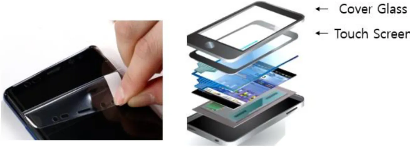
In case of mobile phone, in-display fingerprint recognition is one of the security systems for the bezel-less device. And for portable devices such as smartwatch provides it user recognition without the use of numeric keypad. With the transparent fingerprint sensor it was possible, but some problems appear to adopt the sensor on the screen.
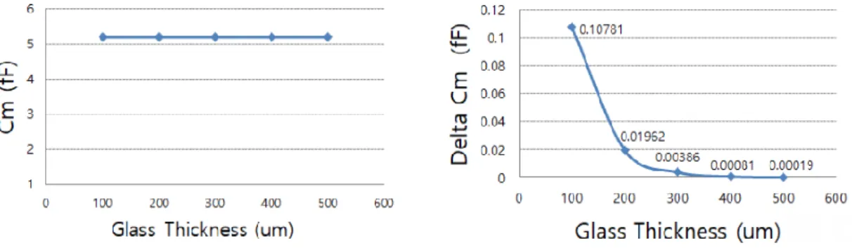
There are other ways of user recognition for mobile devices, such as face ID, optical fingerprint and ultrasonic fingerprint, but they still want to display fingerprint. Cover glass (window) to protect the display panel increases the physical distance of TFPS to user's fingerprint. So, it is necessary to have a high resolution ROIC, because the CVR is very small, but the static capacitance is as large as 5-fF.
Thesis Organization
Research on Conventional ROIC for Mutual Capacitive Sensor
Conventional ROIC
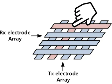
- Self / Mutual Capacitive Sensor for Transparent Fingerprint Recognition
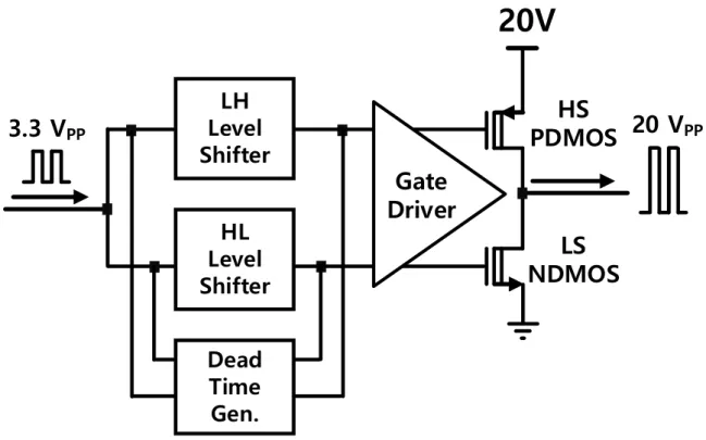
- High Voltage TX Driver
- Lock-in Scheme (RX)
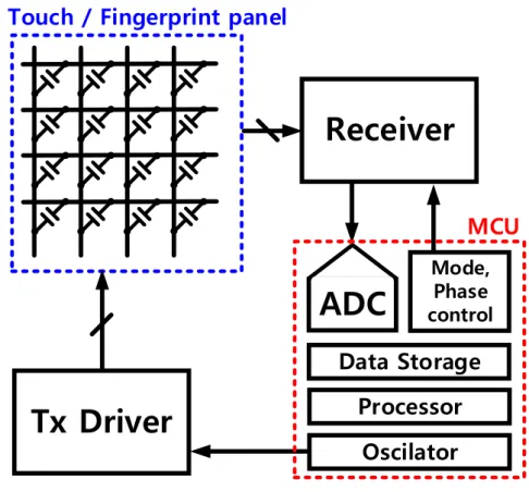
But increasing the number of channels and screen size, the self-capacitive sensor could not get much screen resolution (ppi, pixels per inch). The high voltage Tx driver receives data, such as input frequency and drive mode, from the MCU. The high voltage Tx driver increases the amplitude of the signal when the sensor senses touch and recognizes fingerprints.
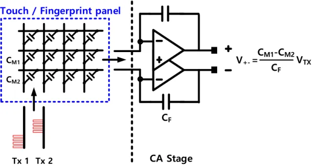
8 The output signal is related to the capacity difference of the adjacent channel @ TISM. Second is the Code Division Multiple Sensing (CDMS) method. And there is no DC offset from two adjacent Tx drivers because the adjacent Tx driver has opposite polarity. And it has advantages of charge amplifier saturation problem, low power consumption and simple circuits compared with CDMS method.
In this thesis, we use the DM-TISM method to drive the sensor and we will compare other Tx steering methods. So the noise of the screen affects the touch and fingerprint sensors with the driving frequency of the screen. It is converted to the output voltage of the charge amplifier, the relative junction capacitance (Cc) and the floating screen driving voltage. [2.5].
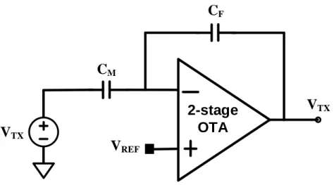
To make this structure of the circuit diagram, it is necessary to analyze the structure of the mutual capacitive sensor and the load amplifier block, the first stage of the receiver. But in case of low feedback capacitor value, there is feedback capacitor process variation problem and load amplifier output node saturation problem. Also, there is the problem of the large feedback resistance value area to make the appropriate cutoff frequency for the passband of the TX signal.
It is possible to cancel global noise as external noise by using fully differentiated structure.
Touch / Fingerprint Environment Noise
Performance Evaluation
First, to detect fingerprint information on the display panel, it is necessary to overcome the cover glass between the finger and the sensor. Considering the latest cover glass thickness of mobile device and the thickness of protective film, it is necessary ROIC to detect the difference of few atto-farads capacitance. Considering these issues, the proposed MCSM method reduces the ROIC area of the receiver around the number of clustered electrodes.
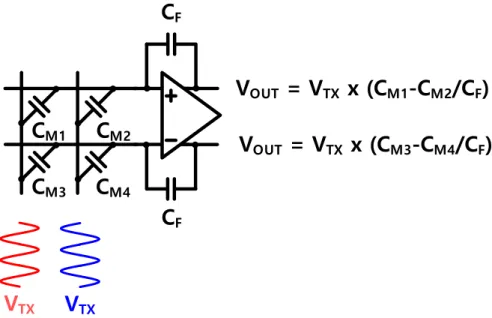
So it is impossible to reduce this AC compensation by lock-in scheme and fully differential structure. In conventional TISM mode TX and RX cases, each charge amplifier output is proportional to CM/CF. To adapt DM-TISM method, each charge amplifier output is proportional to delta CM, not CM.
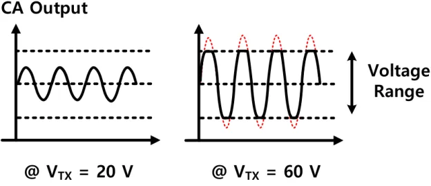
It has a small output swing of the charge amplifier compared to the TISM method, such as few femto-farads. But due to the uniformity problem, it is difficult to reduce CF to less than a few hundred femto-farads. With this DM-TISM method, this thesis suggests an MCSM method to increase the SNR via the noise averaging method.
A proposed ROIC system consists of a modified high-voltage TX driver, Lock-in scheme, a fully differential gain amplifier and MCSM method. In the charge amplifier phase, the signal is amplified via the feedback capacitor to the output of the amplifier. In addition, to control the gain of the charge amplifier stage, a capacitor, which is the same size as the feedback capacitor, is connected in parallel with the feedback capacitor.
The common output is connected to the high-voltage amplitude of the TX signal and the gain of the charge amplifier, the differential gain amplifier and the low-pass filter. An additional differential gain amplifier stage and gain modification can be considered to increase the output amplitude. Adopting the MCSM method therefore results in better SNR and frame rate than recent works without compromising on area and power.
High Resolution Read-out IC for Mutual Capacitive Sensor
Design Issues for High Resolution ROIC in a TFPS
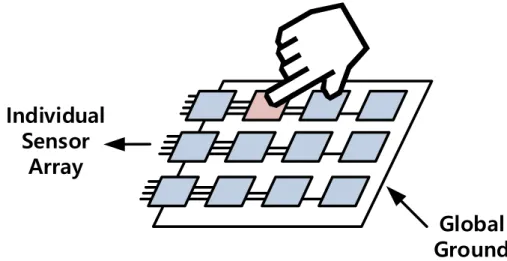
Also, according to the user's taste, additional protective film is one of the reasons to reduce the signal. Secondly, in order to detect fingerprint information, it needs two-dimensional information with standard area and resolution. The increase in the area of 1 ROIC channel of the receiver affects the total area of the entire chip size 100 times more.
Third, the effect of various external noise and ROIC internal noise in the sensor environment on the screen. These noises can be eliminated using lock-in scheme with modulation and demodulation of signal. Fully differential amplifier structure also reduces a lot of common mode noise like VDD and external noise.
Proposed Approach
Given a situation where CONT<0> is high, the equivalent circuit is on the right. One at the left end is delta C1 and one at the right end is delta C6. However, to detect the same number of capacitances, MCSM still has the advantage of SNR and AREA.
The value of Time Area efficiency is highest at MCSM_6 to fuse more electrodes, the efficiency decreases after MCSM_6.
A Proposed Multi Channel Selective Merge (MCSM) System Architecture
The proposed TX driver of ROIC is manufactured by HV BCD 0.18um process for high voltage driving. The HV TX driver consists of buffer, LH switch, HL switch, mode control unit, code generation unit, HS switch and LS switch. To compare with other driving methods, the TX driver adopts the code generator to drive the CDMS method.
RX stage consists of programmed T/G array, charge amplifier, differential amplifier and low pass filter. Also, to detect capacitance variation of the 6th input channel and next ROIC channel's 1st input channel, channel difference detection phase is introduced. In the differential amplifier stage, to satisfy the gain of 30, the gain capacitor and DGA feedback capacitor are introduced.
During demodulation, the time of the cutoff frequency of the next low-pass filter is determined. To meet the frame rate of 40 Hz, the proposed system has a cutoff frequency of 10 us as 5 τ. The DC output signal, after the low-pass filter, goes to ADC and then to the stored MCU.
Simulation Result
Summary
1.1] Beyeong Wan An, et al, "A transparent and flexible fingerprint sensor array with multiplexed sensing of tactile pressure and skin temperature.", Nature Communications, 2018. 2.2] Sanghyun Heo, et al, "Differentially encoded multiple signal method with fully differential TSP Mutual Capacitive Fingerprint Receiver", IEEE Transactions on Circuits and System I: Regular papers, 2019. 2.3] Noriyuki Miura, et al, "1 mm Pitch 80 x 80 Channel 322 Hz Frame-Rate Multitouch Distribution Sensor With Two-Step Dual-Mode Capacitance Scan", IEEE Journal of Solid-State Circuits, vol.
2.4] Jiheon Park, et al, "Touch Readout Mutual Capacitive IC with 64% Reduced Power Adiabatic Driving via Strongly Coupled Touch Screen", IEEE Journal of Solid-State Circuits, vol.