Work function (measured by UPS and KPFM) and conductivity (measured by 4-point probe) of PEDOT:PSS films with and without CD-Ag NPs. Device characteristics of P3HT: PCBM-based PSCs with free Ag NPs and CD-Ag NPs.
Introduction
History of Organic Solar Cells (OSCs)
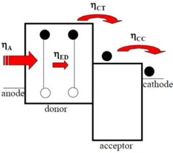
Physics of OSCs
- Principle of OSCs
- Characterization of OSCs
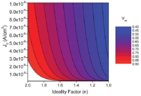
From such curves, open circuit voltage (Voc), short circuit current density (Jsc) and fill factor (FF) can be obtained. Solving for the current density, the string voltage equation (equation 1.3) at J=0 and V= VOC can be derived as equation 1.4.
Development of Polymer Solar Cells (PSCs)
- Molecular designs
- Interfacial engineering
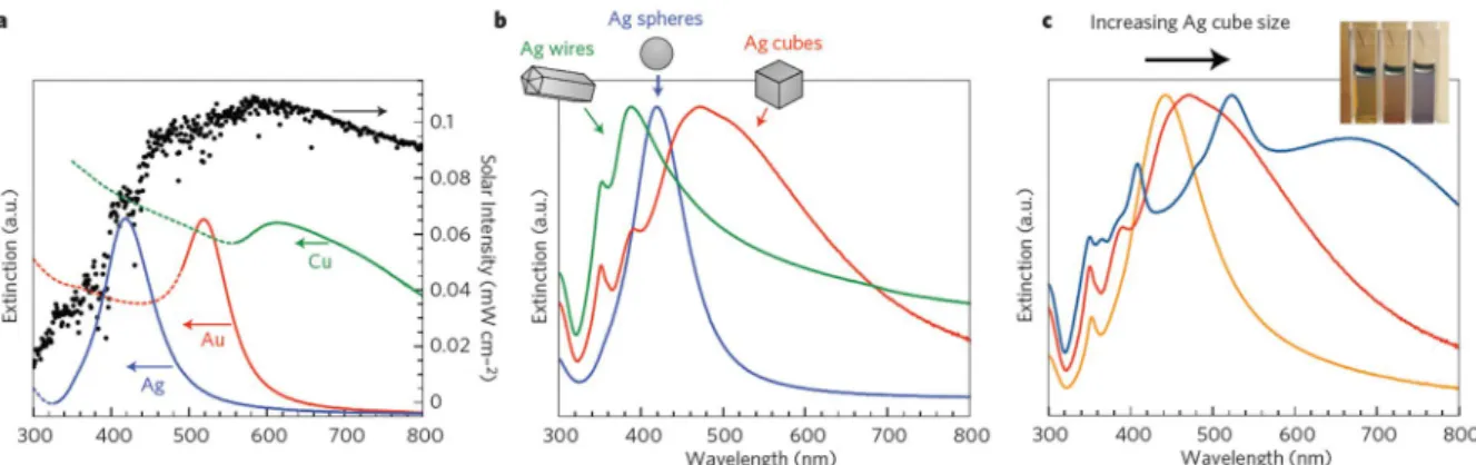
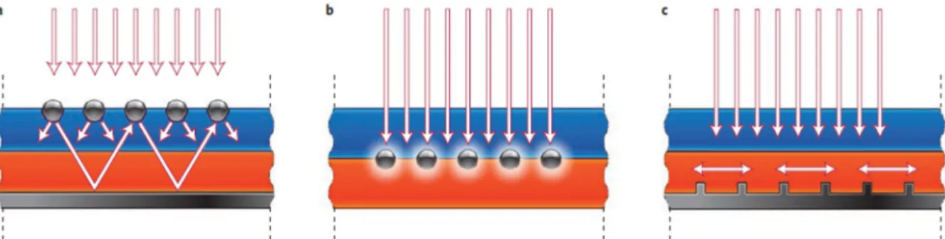
- Surface plasmon resonance effect
In addition, the morphology of the upper active layer is affected by the change in surface energy by SAM. The introduction of a second series of metal nanoparticles or nanodies on the other side of the active layer, as illustrated in Figure 1.15e, led to further improvement in the optical absorption of the active organic layer.
Research Overview and Objective
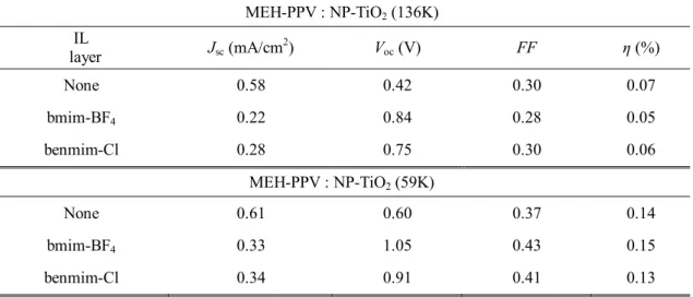
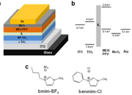
Enhanced Open-Circuit Voltage by Hydrophilic Ionic Liquids in Polymer-Titanium
- Research background
- Experimental
- Results and discussion
- Conclusion
In both MEH-PPV:NP-TiO2 films, the absorption intensity of MEH-PPV decreases slightly with the introduction of the IL layers. This indicates that IL reduces the amount of MEH-PPV that can be penetrated into the pores by flattening the surface of NP-TiO2. Before infiltration treatment, MEH-PPV:NP-TiO2 (136K) films exhibit approximately 60% PL extinction and MEH-PPV:NP-TiO2 (59K) films exhibit 40% PL extinction compared to that of pristine MEH-PPV film .
This indicates that photoinduced charge transfer indeed occurred from MEH-PPV to TiO2. The working principle of MEH-PPV:NP-TiO2 HSC can be described by the following steps. IL layers were used to modify the NP-TiO2 surface to fabricate MEH-PPV:NP-TiO2 HSCs.
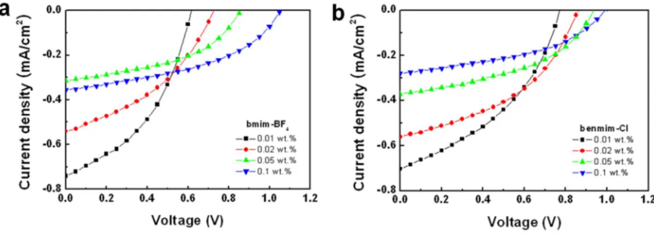
Device features of MEH-PPV: NP-TiO2 based devices with different NP-TiO2 and ionic liquids. The effect of IL concentration on device performance was investigated in MEH-PPV/IL/NP-TiO2 HSCs.
Combination of Titanium Oxide and Conjugated Polyelectrolyte for High-
- Research background
- Experimental
- Results and discussion
- Conclusion
- Research background
- Experimental
- Results and discussion
- Conclusion
The surface properties and morphology of the TiOx films with and without the CPE layer were characterized by contact angle measurements (DSA100) and atomic force microscopy (AFM). The photoluminescence spectra of the TiOx/(CPE)/P3HT films were measured on a Cary Eclipse spectrofluorometer with a xenon lamp excitation source. Chemical structure of CPE, cationic poly(9,9'-bis(6''-N,N,N-trimethylammoniumhexyl)-fluorene-co-alt-phenylene) with bromide counterions (FPQ-Br). b) Schematic energy diagrams for flat band conditions at the TiOx/(CPE)/active layer junction with and without the CPE layer.
In addition, the surface of the TiOx/CPE layer is smoother than the surface of pristine TiOx as confirmed by atomic force microscopy (AFM) (Figure 3.3). The smoother and more hydrophobic surface of the TiOx/CPE layer improves the compatibility between the organic active layer and inorganic TiOx and induces better contact between them. Clearly, the FF value of 0.70 is the highest so far recorded in iPSCs.[15] The CPE layer minimizes the contact resistance between TiOx and the organic active layer due to the improved compatibility between the two layers as confirmed by electrical impedance spectroscopy (Figure 3.6). a) J-V characteristics and (b) EQE of P3HT:PCBM inverted solar cells of FTO/TiOx/(CPE)/active layer/MoO3/Au with and without the CPE layer.
A pronounced PL quenching (∼15%) of PTBT was observed after incorporating bis-FSAMs at the PTBT/TiOX interface compared to that with pristine TiOX. The film with BA-SAM showed negligible PL quenching compared to that without SAM. Topographic images (left side) and contact angle measurements (right side) of (a) pristine TiOX, (b) mono-FSAM, and (c) bis-FSAM thin film on top of the TiOX layer.

Surface plasmon resonance of carbon dot-supported silver nanoparticles: Versatility
Research Background
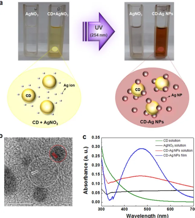
Here, we demonstrate highly efficient PLEDs and PSCs using surface plasmon resonance (SPR) enhancement with CD-supported silver nanoparticles (CD-Ag NPs). First, excellent electron-donating ability of photoexcited CD enables rapid reduction of metal salts to corresponding metal NPs on the surface of CD.289 During this process, the CD also acts as a template, leading to metal NPs- decorated surface of CD. Second, the synthesis of the CD-Ag NPs is simple and requires only basic equipment (i.e., a 20 min exposure to UV lamp).
Third, the aggregation effect of Ag NPs in CD results in extensive light absorption by the increase of the electric field in the gap between Ag NPs without any change of the size and shape of Ag NPs. Fourth, due to their low-temperature solution processability, CD-Ag NPs are compatible with large-area mass production techniques and are suitable for printed electronic devices.
Experimental
Free Ag NPs prepared in this way had an average diameter of 3 nm, equal to the diameters of Ag NPs synthesized with CDs. XPS and Raman spectroscopy: The functional groups of CD and CD-Ag NPs were analyzed by XPS (K-alpha, Thermo Fisher). The size of CD-Ag NPs composites was measured using a JEM-2100F (Cs corrector) high-resolution transmission electron microscope (HR-TEM).
The work function of PEDOT:PSS films with and without CD-Ag NPs were obtained via ultraviolet photoelectron spectroscopy using the He I radiation line (21.22 eV) from a discharge lamp and a Park Systems XE-70 Kelvin Probe force microscope in contactless mode. For fluorescence enhancement experiments, 15 mW of 473 nm output in the diode type was used. In this simulation, we assumed that the Ag NPs were uniformly distributed in the x-y plane of the CD surface and embedded in a background environment of PEDOT:PSS.
The device architecture used for PLEDs and PSCs was ITO/CD-Ag NPs/PEDOT:PSS/emissive or active layer/(LiF)/Al. The electrical properties of the PLEDs were measured using a Keithley 2400 source measurement unit equipped with a Minolta CS2000 under ambient conditions.
Results and Discussion
For comparison, the PEDOT:PSS/SY films with and without CD-Ag NPs on glass substrates were included. The inset in (a) represents confocal scanning microscope images of the SY film (bottom) without and (top) with CD-Ag NPs. We investigated the use of CD-Ag NPs as plasmonic materials in PLEDs and PSCs.
The device structure used was glass/indium tin oxide (ITO)/CD-Ag NPs/PEDOT:PSS/SY/LiF/Al (Figure 5.10a). The device structure used was a glass/ITO/CD-Ag NPs/PEDOT:PSS/PTB7:PC71BM/Al (Figure 5.10e). Device properties of SY-based PLEDs and PTB7:PC71BM-based PSCs with and without CD-Ag NPs.
Photoemission threshold region obtained via UPS for PEDOT:PSS films with and without CD-Ag NPs. The blue and red solid lines indicate the UV-vis absorption of free Ag NPs and CD-Ag NPs, respectively.
Conclusion
Multi-Positional Silica-Coated Silver Nanoparticles for High-Performance Polymer
Research Background
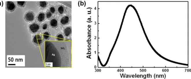
Here, we report high-performance PSCs utilizing the SPR effect via multipositional silica-coated silver NPs (Ag@SiO2). The silica shell in Ag@SiO2 preserves the SPR effect of Ag NPs by preventing oxidation of Ag core under ambient conditions and also eliminates the concern of exciton quenching by avoiding direct contact between Ag cores and the active layer. Multipositional property of Ag@SiO2 originating from silica shell allows it to be introduced at both ITO/PEDOT:PSS (type I) and PEDOT:PSS/active layer (type II) interfaces in polymer:fullerene-based BHJ PSC' is.
Experimental
Compared to bare Ag NPs of the same size (about 50 nm), Ag@SiO2 showed a red-shifted SPR peak at 450 nm caused by silica (Figure 6.3). This result indicates that the active layer as the surrounding matrix has a greater influence on the electric field enhancement of Ag@SiO2 than the PEDOT:PSS layer. More than 150 devices were fabricated to optimize device performance by controlling Ag@SiO2 concentration in PTB7:PC70BM-based PSCs with Type I and Type II (Figure 6.7 and Table 6.2).
Device characteristics of PTB7:PC70BM-based PSCs with types I and II as a function of Ag@SiO2 solution concentration. The device without Ag@SiO2 shows a maximum EQE of 69.4%, while the devices with type I and type II show an improved EQE of 77.3%. The calculated work functions were 5.3 eV for all PEDOT:PSS films with and without Ag@SiO2.
Comparison of the EQE enhancement (Δ EQE) with absorption change (Δ absorption) caused by different Ag@SiO2 position. To compare the effect of Ag@SiO2 and bare Ag NPs on device performance, PTB7:PC70BM-based PSCs were fabricated in which Ag@SiO2 NPs were replaced with bare Ag NPs in both type I and II device architectures.
Conclusion
Summary
Finally, I demonstrated highly efficient inverted polymer solar cells (iPSCs) using fullerene-based self-assembled monolayers (FSAMs) as an interface between the organic active layer and the inorganic TiOX layer. The device with pristine TiOX layer shows an energy conversion efficiency (PCE) of 3.28%, while the device with bis-4-(2-ethylhexyloxy)-[6,6]-phenyl C61-butyric acid (bis-p- EHO-PCBA) shows a remarkably improved PCE of 5.13%. Compared with previous plasmonic materials, CD-Ag NPs led to broad light absorption, originating from the ensemble of plasmon coupling effects caused by the clustering of Ag NPs into CD-Ag NPs.
Furthermore, the incorporation of Ag@SiO2 between the hole transport layer and the active layer led to significant improvement in device efficiency, caused by increased light absorption and scattering through enhanced electric field distribution. In addition, Ag@NMP-based ITO-free PSCs and PLEDs showed improved device performance resulting from the SPR effect and improved electrical conductivity from Ag NPs. The collective surface plasmon ensemble of CD-Ag NPs allows for individual surface plasmon coupling with significant improvement in device performance; thus achieving a greatly improved current efficiency (CE) of 27.16 cd A-1 and luminous efficiency (LE) of 18.54 lm W-1 in PLEDs, and power conversion efficiency (PCE) of 8, 31% in PSC, compared to those of devices without CD-Ag NPs (CE = 11.65 cd A-1 and LE = 6.33 lm W-1 in PLED, and PCE = 7.53 % in PSC).
To our knowledge, this LE in PLEDs with CD-Ag NPs is one of the highest values in fluorescent PLEDs based on the solution process. The device incorporating nanoparticles between the hole transport layer and the active layer achieves a power conversion efficiency of 8.92% with an external quantum efficiency of 81.5%.
6.5% Efficiency of Polymer Solar Cells Based on Poly(3-hexylthiophene) and Indene-C(60) Bisadduct by Device Optimization. Efficient, air-stable Bulk Heterojunction Polymer Solar Cells using Moox as the anode interface layer.
Acknowledgements