저작자표시-비영리-변경금지 2.0 대한민국 이용자는 아래의 조건을 따르는 경우에 한하여 자유롭게
l 이 저작물을 복제, 배포, 전송, 전시, 공연 및 방송할 수 있습니다. 다음과 같은 조건을 따라야 합니다:
l 귀하는, 이 저작물의 재이용이나 배포의 경우, 이 저작물에 적용된 이용허락조건 을 명확하게 나타내어야 합니다.
l 저작권자로부터 별도의 허가를 받으면 이러한 조건들은 적용되지 않습니다.
저작권법에 따른 이용자의 권리는 위의 내용에 의하여 영향을 받지 않습니다. 이것은 이용허락규약(Legal Code)을 이해하기 쉽게 요약한 것입니다.
Disclaimer
저작자표시. 귀하는 원저작자를 표시하여야 합니다.
비영리. 귀하는 이 저작물을 영리 목적으로 이용할 수 없습니다.
변경금지. 귀하는 이 저작물을 개작, 변형 또는 가공할 수 없습니다.
Investigation of Plasmonics Based on Transparent Conducting Oxide
Seong-Min Kang Department of Physics
Graduate School of UNIST
2017
Investigation of Plasmonics Based on Transparent Conducting Oxide
Seong-Min Kang
Department of Physics Graduate School of UNIST
Investigation of Plasmonics Based on Transparent Conducting Oxide
A thesis Submitted to the Graduate School of UNIST
In partial fulfillment of the requirements for the degree of- Master of Science
Seong-Min Kang
01. 19. 2017 of submission Approved by
______________
Advisor
Min-Suk Kwon
Investigation of Plasmonics Based on Transparent Conducting Oxide
Seong-Min Kang
This certifies that the thesis of Seong Min Kang is approved.
01. 19. 2017 of submission Signature
___________________________
Advisor: Min Suk Kwon
Signature
___________________________
Ki bog Park: Thesis Committee Member #1
Signature
___________________________
Min Sup Hur: Thesis Committee Member #2
Abstract
The mid-infrared is the spectral range between 2 m and 20 m. It is useful for chemical, biological, or environmental sensing since molecules have their own absorption spectra, called fingerprints, in the mid-infrared. Surface enhanced infrared absorption is a mechanism which many mid-infrared sensors are based on. It can be usually obtained from a plasmonic resonance around a metal nano-structure.
Transparent conducting oxides (TCOs) behave like a metal in the mid-infrared. TCO nano-particles are superior to metal nano-particles since the former have more strongly confined plasmonic resonance modes than the latter. Therefore, TCO nano-particle arrays may be suitable for mid-infrared sensors.
This thesis theoretically investigates the characteristics of indium-tin-oxide (ITO), which is a representative TCO, nano-particle arrays. The investigated ITO nano-particle arrays can be realized by using plasma surface treatment of a polymer film and deposition of ITO on the film. The array consists of a thin ITO film, a square or hexagonal lattice of ITO circular posts, and ITO nano-spheres sitting on the posts. It is analyzed how the characteristics depend on the diameter of the ITO nano-sphere, the spacing between the adjacent ITO nano-spheres, the dimensions of the post, and the carrier concentration in ITO. The analysis demonstrates that the ITO nano-particle arrays possess strong absorption of more than 50 % in the mid-infrared. The ITO nano-particle arrays may be used as a simply-realizable, low-cost platform for mid-infrared sensors based on surface enhanced infrared absorption.
Contents
Ⅰ. Introduction………...1
1.1 Mid Infrared ……….1
1.2 Surface Enhanced Infrared Absorption ………2
1.3 Dielectric Constant of ITO………3
1.4 Scattering and Absorption of ITO, Au………..4
1.5 ITO-Based SEIRA……….5
1.6 Investigated ITO Nanostructure………6
Ⅱ. ITO nanostructure………..7
2.1 Simulation Model and Parameters……….7
2.2 Square or Hexagonal Lattice Structure & Simulation Setup……….8
Ⅲ. Properties depending on structural parameters………...9
3.1 Transmission, Reflection, and Absorption……….9
3.2 Absorption Spectra Depending on L………11
3.3 Absorption Spectra for rs = 30 and 70nm………..12
3.4 Absorption Spectra Depending on rs………13
3.5 Absorption Spectra Depending on rp and hp……….14
3.6 Absorption Spectra Depending on tf……….15
3.7 Absorption cross section and Scattering cross section Depending on N………..16
3.8 Absorption Spectra Depending on N………17
3.9 Hexagonal Lattice Structure Results……….18
IV. Conclusion………..19
List of Figures
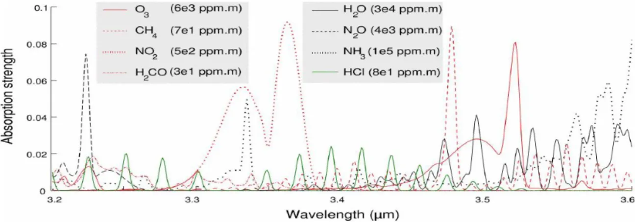
Figure 1-1 Absorption spectra of the 4 gas components present in the mixture (red curves) and of 4 other chemicals of the spectral database (black and green curves). The green curve corresponds to the absorption spectrum of HCL. [1]
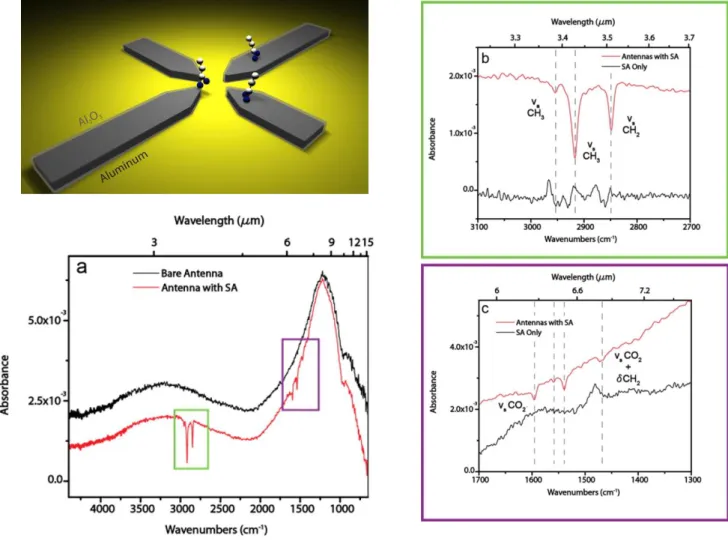
Figure 1-2 Cross section of Asymmetric Aluminum Antenna (a) Comparison of spectra from a 3 x 3 Al antenna array (𝐿1 and 𝐿2 = 1800 and 650nm) before and after stearic acid (SA) functionalization in a 2mM solution. (b) Expanded view of the C-H group region molecular signal on the antennas and a reference spectrum of a stearic acid SAM on bulk aluminum film (scaled for visibility), with prominent vibrations at 2850, 2920, and 2950𝑐𝑚−1 labeled (c) Expanded view of CO vibration region with the vibrations indicated at 1464 and 1592𝑐𝑚−1, as well as a pair of mixed-strength C-O bonds at 1540 and 1560𝑐𝑚−1, indicating different types of bonding between the carboylate headgroup and the alumina surface. [2]
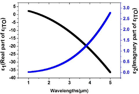
Figure 1-3 Real (ε1, black) and imaginary (ε2, blue) parts of the dielectric function of ITO. ITO material parameters (𝜀∞,𝐼𝑇𝑂 = 3.9, 𝜔𝑝,𝐼𝑇𝑂 = 2.4 × 10¹⁵rad/s, Γ𝐼𝑇𝑂 = 2.6 × 10¹³rad/s)
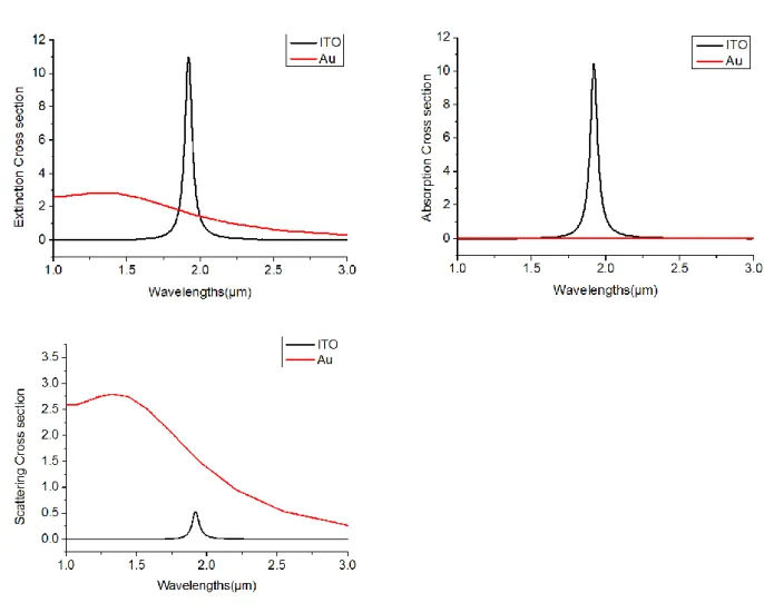
Figure 1-4 (a) Extinction, (b) absorption, (c) scattering cross sections for isolated ITO sphere and Au sphere
Figure 1-5 (a) SEM images of ITO antenna arrays, (b) Infrared transmission spectra of ITO antenna arrays, (c) SEIRS spectra, SEIRS Enhancement
Figure 1-6 (a), (b), (c) FE-SEM images of ITO nano arrays under various conditions (Left figure) High-angle annular-dark-field image of an ITO nanoarray (Right figure)
Figure 2-1 Simulation Model and Parameters rs (sphere radius), rp( post radius), hp(post height), tf( film thickness), L(Period).
Figure 2-2 the top view of the unit cell of square lattice structure and hexagonal lattice structure is shown in Fig.2-2 (a), (c). Schematic view of ITO nanostructure in two cases is shown in Fig.2 (b), (d)
Figure 3-1 (a) Calculated transmission, reflection, absorption forrs = 50 nm, L = 160nm
(Gap = 60nm), rp = 60nm, hp = 40nm, tf = 50nm. (b) Calculated extinction cross section (black, left axis) and absorptance (blue, right axis). (c) Electric field distribution in the xz plane at absorption peak. (d) Electric field distribution in the xy plane at absorption peak.
Figure 3-2 (a),(b) absorption spectra varied with period forrs = 50 nm,rp = 30nm, hp = 40nm, tf =
50nm. (c) Electric field distribution in the xz plane at absorption peak ( = 1.9m) for L=110nm (d) Electric field distribution in the xy plane at absorption peak ( = 2.3m) for L=110nm.
Figure 3-3 (a), (b) absorption spectra varied with period forrs = 30 nm,rp = 10nm, hp = 20nm, tf = 50nm. (c), (d) absorption spectra varied with period forrs = 70 nm,rp = 30nm, hp = 40nm, tf = 50nm.
Figure 3-4 absorption spectra varied with sphere radius for(a) gap = 60nm, (b) gap = 10nm.
Figure 3-5 absorption spectra varied with (a) post radius, (b) post height
Figure 3-6 (a) absorption spectra varied with film thickness for rs = 50 nm, L = 150nm, rp = 30nm, hp
= 40nm, tf = 50nm. (b) Electric field distribution in the xz plane at absorption peak ( = 1.9m) for L=150nm. (c) Electric field distribution in the xy plane at absorption peak ( = 2.3m) for L=150nm.
Figure 3-7 Extinction, absorption, scattering cross sections for isolated ITO sphere varied with carrier concentration.
Figure 3-8 Extinction, absorption, scattering cross sections for isolated ITO sphere varied with carrier concentration for(a) gap = 10nm, (b) gap = 60nm.
Figure 3-9 absorption spectra varied with period for (a) hexagonal structure, (b) square structure.
(R=50nm).
Nomenclature
Mid-IR Mid-Infrared
SEIRA Surface Enhanced Infrared Absorption
ITO Indium Tin Oxide
SEM Scanning electron microscope
FDTD Finite difference time domain
PML Perfectly matched layer
LSPR Localized surface plasmon resonance
Chapter1. Introduction 1.1 Mid-Infrared
The mid-infrared is the spectral range between 2 m and 20 m. It is useful for chemical, biological, or environmental sensing since molecules have their own absorption spectra, called fingerprints, in the mid-infrared. The mid-infrared spectral region contains strong characteristic vibrational transitions of many important molecules. Recently, selectivity molecular detection at nanoscale level in fingerprint region is in great demand for various applications.[1] Complex vibrational characteristics of molecules in bulk materials can be effectively distinguished to enable unambiguous identification of molecular structures and species [1],[2]. Fig. 1.1 show absorption spectra of diverse chemicals [1]. The mid- infrared spectroscopy take advantage of diverse areas such as thermal imaging and chemical sensing.
Especially, Mid-infrared spectroscopy is a widely used technique for material identification in chemical sensing. The enhancement of vibrational modes of molecules in the infrared “chemical fingerprinting”
region of the spectrum, known as Surface-enhanced infrared absorption (SEIRA) spectroscopy, is a topic of rapidly increasing interest. Surface enhanced infrared absorption is a mechanism which many mid-infrared sensors are based on. It can be usually obtained from a plasmonic resonance around a metal nano-structure.
Fig. 1.1. Absorption spectra of the 4 gas components present in the mixture (red curves) and of 4 other chemicals of the spectral database (black and green curves). The green curve corresponds to the absorption spectrum of HCL. [1]
1.2 Surface Enhanced Infrared absorption
SEIRS is a spectroscopic technique used to identify molecular fingerprints by resonant detection of infrared vibrational modes through coupling with the plasmonic modes of an antenna. [3]
SEIRA is based on the coupling between IR vibrational modes and plasmonic modes. Nanoparticle Antenna arrays can be using the application for identification of molecular fingerprints. [3] In specific wavelengths it is occur resonance peak. Figure. 1.2 show cross section of Asymmetric Aluminum Antenna for self-Calibrating Surface-Enhanced Infrared absorption Spectroscopy. [4]
Fig. 1.2. Cross section of Asymmetric Aluminum Antenna for Self-Calibrating Surface- Enhanced Infrared Absorption Spectroscopy (a) Comparison of spectra from a 3 x 3 Al antenna array (𝐿1 and 𝐿2 = 1800 and 650nm) before and after stearic acid (SA) functionalization in a 2mM solution. (b) Expanded view of the C-H group region molecular signal on the antennas and a reference spectrum of a stearic acid SAM on bulk aluminum film (scaled for visibility), with prominent vibrations at 2850, 2920, and 2950𝑐𝑚−1 labeled (c) Expanded view of CO vibration region with the vibrations indicated at 1464 and 1592𝑐𝑚−1, as well as a pair of mixed-strength C-O bonds at 1540 and 1560𝑐𝑚−1, indicating different types of bonding between the carboylate headgroup and the alumina surface. [4]
1.3 Dielectric Constant of ITO
Dielectric function is given by Drude model. Also, plasma frequency is expressed by the function of carrier concentration. When the carrier concentration is changed, optical properties are changed. In addition, Transparent conducting oxides (TCOs) behave like a metal in the mid-infrared. So TCO may be suitable for mid-infrared sensors.
𝜀𝐼𝑇𝑂 = 𝜀∞− 𝜔𝑝2 𝜔2+ 𝑖𝜔𝛤
Dielectric function of ITO is given by Drude model. 𝜀𝐼𝑇𝑂 is permittivity of ITO, 𝜔𝑝 is the plasma frequency, 𝛤 is relaxation rate.
𝜔𝑝2= 𝑁𝑞2 𝜀∞𝑚∗
Plasma frequency is given by the function of carrier concentration. N is carrier concentration, q is electron charge, 𝑚∗is effective electron mass.
(1.1)
(1.2)
Fig. 1-3.Real (ε1, black) and imaginary (ε2, blue) parts of the dielectric function of ITO obtained using Drude model fittings to experimental data from Johnson and Christy. ITO material parameters (𝜀∞,𝐼𝑇𝑂 = 3.9, 𝜔𝑝,𝐼𝑇𝑂 = 2.4 × 10¹⁵rad/s, Γ𝐼𝑇𝑂= 2.6 × 10¹³rad/s)
1.4 Scattering and Absorption – ITO vs Au
As simulation results, Fig. 1-4 show spectrum of extinction, absorption, scattering cross section with isolated ITO sphere and Au sphere in wavelength region from 1m to 3m. In case of Au sphere, it has large radius for the plasmonic mode. And then extinction mainly is caused by scattering in Au sphere.
In case of the Au sphere, it is not occur effectively absorption. Comparing to ITO sphere, Au sphere have smaller absorption cross section than ITO sphere in Mid-IR. But extinction mainly is caused by absorbing in ITO sphere. So ITO nanoparticles are more suitable for SEIRA than Au nanoparticles.
Fig. 1-4 (a) Extinction, (b) absorption, (c) scattering cross sections for isolated ITO sphere and Au sphere
1.5 ITO-Based SEIRA
In the content of the reference papar [3], Fig. 1.5 show SEM images of ITO antenna arrays with with L
= 0.5 m for spacings s = 600nm and s = 300nm.[3] Fig. 1.5(b) show Infrared transmission spectra of ITO antenna arrays dependent on array geometries presented in (a) and for various nanorod lengths L.[3]
Transparent conducting oxides (TCOs) are large bandgap dielectric with a density of free carriers in between that of doped semi-conductors and noble metals. [3] So Optical property of ITO nano-particle arrays can be utilized in diverse areas such as sensing, spectroscopy. Also, ITO-Based SEIRA can be used in a variety of areas such as sensing, spectroscopy.
Fig. 1-5. (a) SEM images of ITO antenna arrays with L = 0.5 m for spacings s = 600nm (i) and s = 300nm (ii). (b) Infrared transmission spectra of ITO antenna arrays corresponding to typical array geometries presented in (a) and for various nanorod lengths L. The arrays were covered with a 50nm PMMA layer, resulting in sharp SEIRS features due to plasmon coupling with vibrational resonances. [3]
Nano Lett.14, 346 (2014)
(b)
(a) (c)
1.6 Investigated ITO Nanostructure
In reference paper, Fig. 1-6 (a) schematically show FE-SEM images demonstrating the evolution of the ITO nanoarrays on the surfaces of polymer substrates that were pretreated under various condition.[5]
Fig. 1-6 (b) (left figure) show a compact ITO nanoarray on a polymer surface that was pretreated for a relatively short period of 1min.[5] In Fig. 1-6 (c), it is shown for a loose ITO nanoarray on a polymer surface that was pretreated for an extended period of 3 min.[5] The investigated ITO nano-particle arrays can be realized by using plasma surface treatment of a polymer film and deposition of ITO on the film.
ACS Appl. Mater. Interfaces 5, 164 (2013)
Fig. 1-6. (Left) FE-SEM images demonstrating the evolution of the ITO nanoarrays on the surfaces of polymer substrates (a) a continuous ITO layer on a pristine, untreated polymer surface, (b) a compact ITO nanoarray on a polymer surface that was pretreated for a relatively short period of 1 min, and (c) a loose ITO nanoarray on a polymer surface that was pretreated for an extended period of 3 min. (Right) high-angle annular-dark-field image of an ITO nanoarray coated on a PET surface. [5]
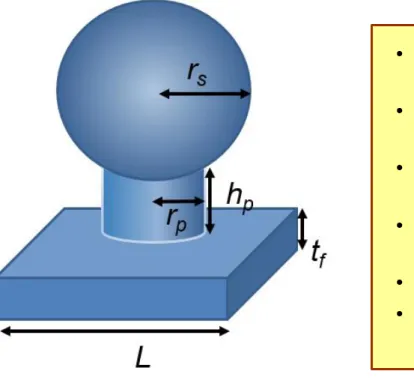
2.1 Simulation Model and Parameter
It is given by parameter which are rs (sphere radius), rp(post radius), hp(post height), tf(film thickness), (Period). Gap between ITO nanoparticles is expressed by Lgap= L - 2r.
As changed by the parameters, we analyze the absorption spectrum of ITO nanostructure. The array consists of a thin ITO film, a square or hexagonal lattice of ITO circular posts, and ITO nano-spheres sitting on the posts. It is analyzed how the characteristics depend on the diameter of the ITO nano- sphere, the spacing between the adjacent ITO nano-spheres, the dimensions of the post, and the carrier concentration in ITO
Fig. 2-1 Simulation Model and Parameters
rs (sphere radius), rp( post radius), hp(post height), tf ( film thickness), L(Period)
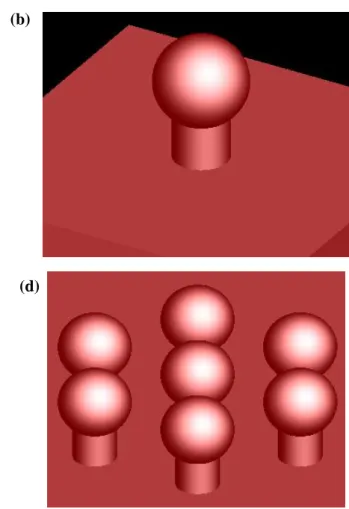
2.2 Square or Hexagonal Lattice Structure
We simulate that absorption spectrum of a periodic array of ITO nanostructure in two cases which are square and hexagonal structure. The top view of the unit cell of square lattice structure and hexagonal lattice structure is shown in Fig.2-2 (a), (c). Schematic view of ITO nanostructure in two cases is shown in Fig.2 (b), (d). We analyzed how the characteristics depend on the ITO nano-sphere, the spacing between the adjacent ITO nano-spheres, the dimensions of the post , and the carrier concentration in ITO. The finite difference time-domain method (FDTD Solutions, Lumerical Inc.) was used for simulations. Fine mesh sizes of 1nm in ITO structure region were used to ensure convergence. Normal incident plane wave source was used to the simulation. It is broadband light from 0.3m to 5m. We applied periodic boundary condition in x, y direction and PML (perfectly matched layer) boundary condition in z direction.
Unit cell
Unit cell
(b)
(c) (d)
(a)
Fig. 2-2 (a) Unit cell of square lattice of ITO (b) Square lattice structure (c) Unit cell of hexagonal lattice of ITO (d) Hexagonal lattice structure
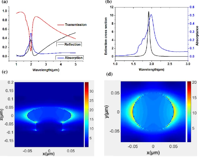
3.1 Transmission, Reflection, and Absorption of ITO nanostructures
Fig. 3-1 (a) shows spectrum of calculated transmission, reflection, absorption in ITO nanostructure for rs = 50nm,L = 160nm (Lgap = 60nm), rp = 60nm, hp = 40nm, tf = 50nm.
As can be seen from Fig.3-1(a), the peak wavelength position of transmission, reflection, absorption spectrum correspond approximately. Fig. 3-1 (b) shows spectrum of calculated extinction cross section and absorption. The peak wavelength position of spectrum of extinction cross section and absorption is a bit of a difference, but the peak wavelength position is similar to wavelength region.
As shown for Fig. 3-1 (b), the resonant peak position of extinction cross section for ITO is related to the carrier concentration. Fig. 3-1 (c) shows electric field distribution in the xz plane at absorption peak.
Fig. 3-1 (a) Calculated transmission, reflection, absorption for rs = 50 nm, L = 160nm
(Gap = 60nm), rp = 60nm, hp = 40nm, tf = 50nm. (b) Calculated extinction cross section (black, left axis) and absorptance (blue, right axis). (c) Electric field distribution in the xz plane at absorption peak. (d) Electric field distribution in the xy plane at absorption peak.
(c) (d)
(b) (a)
(d) (c)
A strong electromagnetic field is induced in both sides of the ITO structure. The localized surface plasmon resonance occur in both sides of the ITO structure. The field pattern with dipole resonance is similar to that when LSPR is excited, which is occurred by oscillating plasmons and strongest field.[6], [8] Fig. 3-1 (d) shows electric field distribution in the xy plane at absorption peak. A strong electromagnetic field is induced in both sides of the ITO structure. Also, the localized surface plasmon resonance occur in both sides of the ITO structure.[9] The LSPR occurred from this structure is similar to dipole resonance.
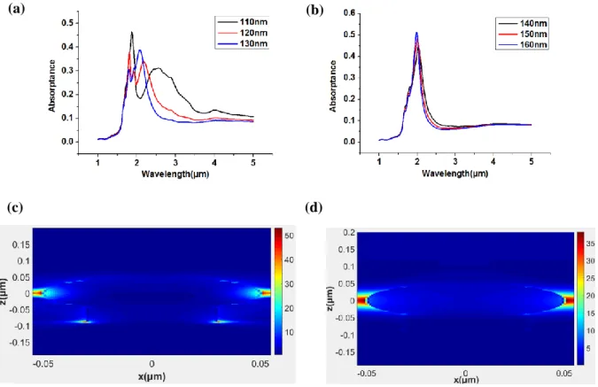
3.2 Absorption Spectra Depending on period (L)
Fig. 3-1 show absorption spectra varied with period for rs = 50nm, rp = 30nm, hp = 40nm, tf = 50nm.
It is shown that the resonance peak is separated to the two resonance wavelengths when the period is below 130nm. To understand the behavior of the absorption peak, we check the electromagnetic field profile at resonance wavelengths. Fig. 3-1 show the electromagnetic field distribution at = 1.9m,
= 2.3m. The strong absorption at resonance wavelengths show the strong local field enhancement when dipole resonance is excited in both sides of the ITO structure.
(b) (a)
(d) (c)
Fig. 3-2 (a), (b) absorption spectra varied with period for rs = 50 nm, rp = 30nm, hp = 40nm,
tf = 50nm. (c) Electric field distribution in the xz plane at absorption peak ( = 1.9m) for L=110nm. (d) Electric field distribution in the xy plane at absorption peak ( = 2.3m) for L=110nm.
(c) (d)
3.3 Absorption Spectra for r
s= 30 nm and 70 nm
It was shown for absorption spectrum with varied period when sphere radius is 30nm and 70nm in Fig. 3-2. As shown in Fig. 2-5 (a), the resonance peak is blue shifts when period between
nanoparticles increase from 70nm to 90nm. But we show that the resonance peak nearly doesn’t change when period between nanoparticles increase 100nm to 120nm in Fig. 2-5 (b). We analyze that resonance wavelengths nearly doesn’t change because particle to particle interaction is weak when period is above 100nm. In addition, as shown in Fig. 3-2 (c), we show that the resonance peak nearly doesn’t change when period between nanoparticles increase 180nm to 200nm. But, we analyze that resonance wavelengths largely doesn’t change because particle to particle interaction is weak when period is above 180nm. And then, as shown in Fig.3-2 (b), (d), it is shown for the one resonance peak when gap between nanoparticles is above about 40nm. On the other hand, when gap is smaller than about 40nm in case of Fig. 3-2 (a), (c), it is shown for the two resonance peak.
(d) (b)
(c) (a)
Fig. 3-3 (a), (b) absorption spectra varied with period for rs = 30 nm, rp = 10nm, hp = 20nm, tf = 50nm.
(c), (d) absorption spectra varied with period for rs = 70 nm, rp = 30nm, hp = 40nm, tf = 50nm.
3.4 Absorption Spectra Depending on r
sFig. 3-4 (a) show the absorption spectra with varied sphere radius when gap length is fixed at Lgap = 60nm. Fig. 3-4 (b) show the absorption spectra with varied sphere radius when gap length is fixed at Lgap = 10nm. Fig. 3-4 (c) show resonance peak position with varied sphere radius when gap length is fixed at Lgap = 60nm.The resonance wavelength is redshift when sphere radius is increase from 30nm to 70nm. In case of Lgap = 10nm, the resonance wavelengths also is redshift when sphere radius is increase from 30nm to 70nm.
(d) (b)
(c) (a)
Fig. 3-4 (a), (b) absorption spectra varied with period at Lgap = 60nm, Lgap = 10nm. (c), (d) resonance peak position varied with sphere radius at Lgap = 60nm, Lgap = 10nm.
3.5 Absorption Spectra Depending on t
fFig. 3-5 is shown for the absorption spectra varied with (a) post radius, (b) post height.
As indicated for Fig. 3-5, we analyze that the influence of rp or hp on the resonance is weak.
Fig. 3-5 absorption spectra varied with (a) post radius, (b) post height
(b) (a)
3.6 Absorption Spectra Depending on t
fIt was shown for absorption spectra varied with film thickness for rs = 50 nm, L = 150nm, rp = 30nm, hp = 40nm, tf = 50nm. It is shown for the one resonance peak when film thickness is below 100nm.
But it is shown that the resonance peak is separated to the two resonance wavelengths when film thickness is above 150nm. Fig. 3-6(b), (c) is shown for the electromagnetic field distribution at = 1.9m, = 2.3m. The strong selective absorption at resonance wavelengths show the strong local field enhancement when dipole resonance is excited in both sides of the ITO structure. The geometric effects on the LSPR obviously show that the peak wavelengths of selective strongly depend on the period of the nanoparticles.[6], [7], [9]
Fig. 3-6 (a) absorption spectra varied with film thickness for rs = 50 nm, L = 150nm,
rp = 30nm, hp = 40nm, tf = 50nm. (b) Electric field distribution in the xz plane at absorption peak ( = 1.9m) for L=150nm. (c) Electric field distribution in the xy plane at absorption peak ( = 2.3m) for L=150nm.
(c) (d)
Electric field distribution at = 1.9m
Electric field distribution at = 2.7m
(b)
(c) (a)
3.7 Absorption and Scattering Depending on N
Extinction, absorption, scattering cross sections are shown in Fig. 3-7 (a), (b), (c) for isolated ITO sphere varied with carrier concentration. Carrier concentration of N2, N4, N6 is 2 × 10²⁰, 4 × 10²⁰, 6 ×
𝑵𝟐: 𝟐 × 𝟏𝟎
𝟐𝟎𝒄𝒎
−𝟑𝑵𝟒: 𝟒 × 𝟏𝟎
𝟐𝟎𝒄𝒎
−𝟑𝑵𝟔: 𝟔 × 𝟏𝟎
𝟐𝟎𝒄𝒎
−𝟑Fig. 3-7 (a) Extinction, (b) absorption, (c) scattering cross sections for isolated ITO sphere varied with carrier concentration.
1020(𝑐𝑚−3). When the carrier concentration is increase, resonance peak wavelengths is blue shift. It is related to permittivity of ITO. Real part of dielectric function of ITO is shift in the short wavelength region.
3.8 Absorption Spectra Depending on N
Fig. 3-8 show the spectrum of extinction, absorption, scattering cross sections for isolated ITO sphere varied with carrier concentration for (a) gap = 10nm, (b) gap = 60nm. It is shown for the two resonance peak when gap length between nanoparticles is 10nm. On the other hand, it is shown for the one resonance peak when gap length is 60nm. In both cases which is spectrum at gap = 10nm, gap = 60nm, the resonance peak is blue shifts when the carrier concentration is increase from 2 × 10²⁰/𝑐𝑚−3 to 6 × 10²⁰/𝑐𝑚−3.
𝑵𝟐: 𝟐 × 𝟏𝟎
𝟐𝟎𝒄𝒎
−𝟑𝑵𝟒: 𝟒 × 𝟏𝟎
𝟐𝟎𝒄𝒎
−𝟑𝑵𝟔: 𝟔 × 𝟏𝟎
𝟐𝟎𝒄𝒎
−𝟑Fig. 3-8 Extinction, absorption, scattering cross sections for isolated ITO sphere varied with carrier concentration for (a) gap = 10nm, (b) gap = 60nm.
We analyze that resonance wavelengths nearly doesn’t change because particle to particle interaction is weak when gap length is 60nm. But compared to absorption spectrum at gap = 60nm, resonance wavelengths is split because particle to particle interaction is relatively stronger. We know that absorption spectrum have strong dependence on gap length between particles. [15], [16]
3.9 Hexagonal Lattice Structure Results
Comparing hexagonal structure to square structure, it is similar the absorption spectrum in two cases.
But we show that the resonance peak nearly doesn’t change when period between nanoparticles increase 140nm to 160nm in Fig. 3-9 (b). We analyze that resonance wavelengths nearly doesn’t change because particle to particle interaction is weak when period is above 100nm. So it is shown for the one resonance peak when gap between nanoparticles is above about 40nm. On the other hand, when gap is smaller than about 40nm in case of Fig. 3-9 (a), (b), it is shown for the two resonance peak.
Fig. 3-9 absorption spectra varied with period for (a) hexagonal structure, (b) square structure. (R=50nm)
We analyze that absorption spectra have dependence on period due to effects of interaction between nanoparticles.
4. Summary & Conclusion
It can be usually obtained from a plasmonic resonance around a metal nano-structure. Transparent conducting oxides (TCOs) behave like a metal in the mid-infrared. TCO nano-particles are superior to metal nano-particles since the former have more strongly confined plasmonic resonance modes than the latter. Therefore, TCO nano-particle arrays may be suitable for mid-infrared sensors. This thesis theoretically investigates the characteristics of indium-tin-oxide (ITO), which is a representative TCO, nano-particle arrays. The investigated ITO nano-particle arrays can be realized by using plasma surface treatment of a polymer film and deposition of ITO on the film. The array consists of a thin ITO film, a square or hexagonal lattice of ITO circular posts, and ITO nano-spheres sitting on the posts. It is analyzed how the characteristics depend on the diameter of the ITO nano-sphere, the spacing between the adjacent ITO nano-spheres, the dimensions of the post, and the carrier
concentration in ITO. We analyzed that resonance wavelengths nearly doesn’t change because particle to particle interaction is weak when gap length is 60nm. But compared to absorption spectrum at gap
= 60nm, resonance mode are split because particle to particle interaction is relatively stronger. We figure out that absorption spectrum have strong dependence on gap length between particles. Also, depending on post radius or post height of ITO nanostructure, resonance peak position is changed little. Though these results, we recognize the influence of post radius or post height on the resonance is weak. When the film thickness is above 100nm, resonance mode are split. When the carrier concentration is increase, resonance peak position is blue shift. It is related to permittivity of ITO. If the carrier concentration is increase, real part of dielectric function of ITO is shift in the short wavelength region. So its characteristics can be tuned by controlling the carrier concentration.
Comparing hexagonal structure to square structure, it is similar the absorption spectrum in two cases.
Absorption spectra have dependence on period due to effects of interaction between ITO
nanoparticles. The analysis demonstrates that the ITO nano-particle arrays possess strong absorption of more than 50 % in the mid-infrared. The ITO nano-particle arrays may be used as a simply- realizable, low-cost platform for mid-infrared sensors based on surface enhanced infrared absorption.
REFERENCES
1. Julien Fade, Sidonie Lefebvre, and Nicolas Cezard, Minimum Description Length approach for unsupervised spectral unmixing of multiple interfering gas species, OPTICS EXPRESS Vol. 19, No. 15
2. Hai Hu, Xiaoxia Yang, Feng Zhai, Far-field nanoscale infrared spectroscopy of vibrational fingerprints of molecules with graphene plasmons. nature communications7, Article number:
12334 (2016)
3. Martina Abb., Yudong Wang, Nikitas Papasimakis, Surface-Enhanced Infrared Spectroscopy Using Metal Oxide Plasmonic Antenna Arrays. Nano Letters, 2014, 14 (1)., pp 346-352
4. Benjamin Cerjan, Xiao Yang, Peter Nordlander, ACS Photonics, 2016, 3(3), pp 354-360 Asymmetric Aluminum Antennas for Self-Calibrating Surface-Enhanced Infrared Absorption Spectroscopy
5. Jungheum Yun, Yeon Hyun Park, Tae-Sung Bae, ACS Appl. Mater. Interfaces 5, 164 (2013) Fabrication of a Completely Transparent and Highly Flexible ITO Nanoparticle Electrode at Room Temperature.
6. Hao wang, Kieran O’Dea, and Liping Wang*, Selective absorption of visible light in film- coupled nanoparticles by exciting magnetic resonance, Optics letter Vol. 39, No.6 (2014)
7. C. Hagglund, G. Zeltzer, R. Ruiz, Thomann, H. Lee, M. L. Brongersma, and S. F. Bent, Self – Assembly Based Plasmonic Arrays Tuned by Atomic Layer Deposition for Extreme Visible Light Absorption Nano Lett. 13, 3352(2013).
8. E. Hutter and J. H. Fendler, Adv. Mater. 16, 1685 (2004).
9. J. Dai, F. Ye, Y. Chen, M. Muhammed, M. Qiu, and M. Yan, Light absorber based on nano- sphere on a substrate reflector, Opt. Express 21, 6697 (2013)
10. C. Ciraci, R. T. Hill, A. Degiron, S. Zauscher, A. Chillkoti, and D. R. Smith, Probing the
Ultimate Limits of Plasmonic Enhancement, Smith, Science 337, 1072 (2012).
11. E. D. Palik, Handbook of Optical Constants of Solids (Academic, 1985) .
12. Z. M. Zhang, Nano/Microscale Heat Transfer (McGraw-Hill, 2007).
13. S. A. Maier, Plasmonics: Fundamentals and Applications (Springer, 2007).
14. Stephanie Law, Lan Yu, All-semiconductor Plamonic Nanoantennas for Infrared Sensing, Nano Lett., 2013, 13 (9), pp 4569-4574
15. Moskovits, M. Rev. Mod. Surface-enhanced spectroscopy Phys 1985, 57, 783-826
16. Naomi J. Halas, Surbhi Lal , Plasmons in Strongly Coupled Metallic Nanostructures, Chem. Rev. 2011. 111 (6). pp3913-3961
![= 0.5 m for spacings s = 600nm and s = 300nm.[3] Fig. 1.5(b) show Infrared transmission spectra of ITO antenna arrays dependent on array geometries presented in (a) and for various nanorod lengths L.[3]](https://thumb-ap.123doks.com/thumbv2/123dokinfo/10529623.0/16.892.97.787.464.888/spacings-infrared-transmission-spectra-antenna-dependent-geometries-presented.webp)
![Fig. 1-6 (b) (left figure) show a compact ITO nanoarray on a polymer surface that was pretreated for a relatively short period of 1min.[5] In Fig](https://thumb-ap.123doks.com/thumbv2/123dokinfo/10529623.0/17.892.116.532.400.829/figure-compact-nanoarray-polymer-surface-pretreated-relatively-period.webp)