Outline
Theoretical background
- Surface Plasmon Polaritons
- Localized Surface Plasmons
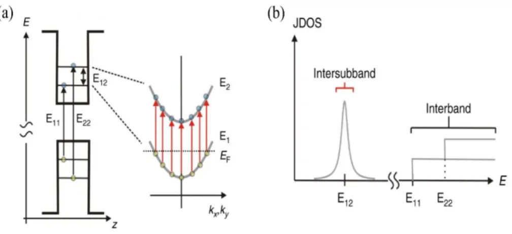
- Intersubband Transitions in a Quantum Well
- Nonlinear Optical Properties from Intersubband Transition
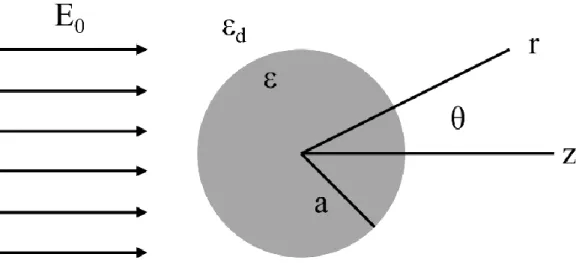
When the external field is applied to the dielectric material, the electrons and the nucleus have polarization. These EM surface waves are excited through the coupling of the free electron plasma oscillation and the EM field. The simplest case of SPPs is shown in Figure 2.2, which is the interface between metal and dielectric.
To obtain the dispersion relation in SPP, we assume that the incident wave is a transverse magnetic (TM) mode. When the TM mode wave is incident light, the plasmons are confined to the surface and can propagate across the surface. This resonance is the LSP and leads to field amplification within and in the near field outside the particles.
Finally, we get the absorption coefficient of IST when the incident wave is TM polarization (𝑒̂ = 𝑧̂). When the fermi level is between E1 and E2, the absorption coefficient is proportional to the doping concentration. The above black line means the conduction band of a quantum well and the other means the valance band of a quantum well.
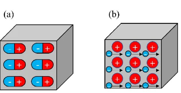
The transition is generated when the incident light is polarized along the direction of quantum confinement and the n quantum well is doped. Nonlinear optics (NL) describes the characteristic of light in nonlinear media, whose constituent parameters are a function of the applied field. Second harmonic generation (SHG) is one of the frequency mixing processes, which generates light at twice the frequency of the incident light.
The black dashed and solid lines represent the energy states of the electrons, and the colored arrows show the transition in the energy states. Therefore, the orientation of the nonlinear materials and the polarization of the incident field must be taken into account. Iω is the intensity of the input source, χ(2) is the second-order sensitivity, and d is the thickness of the nonlinear medium.
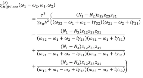
However, the second-order nonlinear susceptibility from IST[30] is about 104 times that of a conventional nonlinear material and can be expressed as .
Electrically reconfigurable difference-frequency-generation from polaritonic metasurface
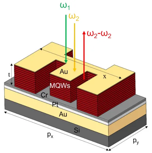
Design of Multiple Quantum Well and Polaritonic Metasurface
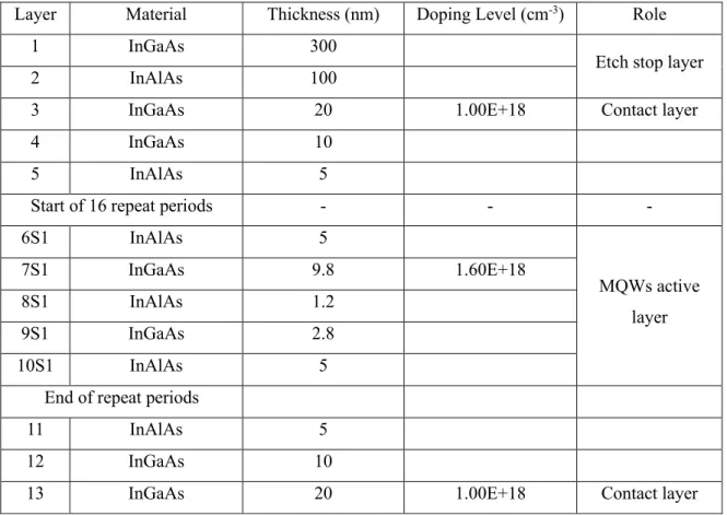
We designed the MQWs using the self-consistent Schrodinger-Poisson solver [40], which calculated under three equations iteratively. V(z), φn(z) and n(z) are calculated by self-consistent Schrodinger-Poisson solver, and Figure 3.1 shows the results of the MQWs for DFG. The MQWs have an asymmetric structure where the first well width is much larger than the second well.
The conduction band is tilted when the external bias is applied to the MQWs by a quantum-confined Stark effect. Therefore, the energy states of the first well (Figure 3.1), which has a larger well width, change larger than the second well. We calculated the permittivity of the above MQWs after designing and fabricating the MQWs for the DFG.
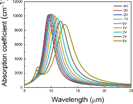
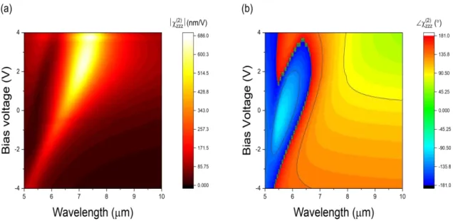
Permissibility depends on IST energy and IST energy is changed by QCSE. On the other hand, the graphs shift to shorter wavelengths (blue shift) when the applied voltage decreases. After calculating the permittivity of the MQWs, we can also calculate the absorption coefficient of the MQWs and Figure 3.2.3 shows the result.
In the case of values of wavelength around 6 μm and 10.6 μm, large and narrow absorption are calculated. Therefore, not only the magnitude of nonlinear second-order sensitivity, but also the phase of nonlinear second-order sensitivity is changed by external bias. In the second-order susceptibility equation, the complex terms make the phase shift.
When the external bias voltage increases, the second-order sensitivity of the MQW also increases. The peak value shifts to a longer wavelength when the external bias voltage increases. The second-order sensitivity of MQWs depends on the external bias voltage, so we can design electrically reconfigurable nonlinear metasurface.
Simulation and Calculation of Nonlinear Optical Responses
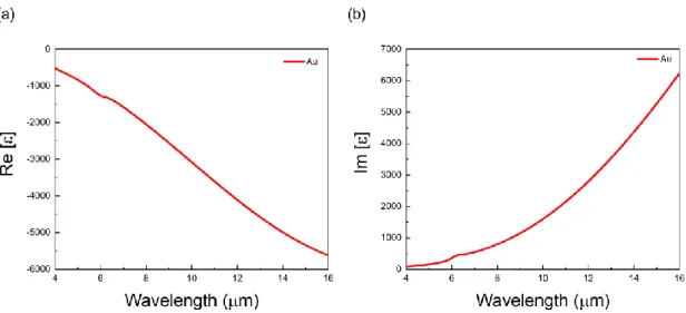
The permittivity of gold (Au) is modeled by the Drude model (equation 2.9) and entered into the program called 'Au (Gold) - Palik'. The permittivity of the MQWs (Figure 3.2.2), which we have already calculated with the Lorentz oscillator model, is entered into the software. The external bias voltage was from −4 V to +4 V and the polarization of the light is (a) x-polarization and (b) y-polarization.
We know that when the external bias voltage is increased, the wavelength is also increased by QCSE from the Figure 3.2.2. However, in Figure 3.3.3 (b), the peak is not greatly changed when the external bias voltage is applied to the DFG metasurface. As we can see the equation 2.25, the intensity of DFG is proportional to the effective second order susceptibility.
From the FDTD simulation, we also simulated the E field on the DFG metasurface and calculated the field broadening factors ( On the other hand, when the light (6.1 μm) is y-polarized, the Ez field induced the side and bottom of the T shape. The largest size The second-order sensitivity peak is 207.336 nm/V when the external bias voltage is 0 V and the wavelength is 6.25 μm.
However, when the external bias is applied to the DFG metasurface, the effective second-order sensitivity is reduced. This is because the second-order sensitivity of MQWs and field enhancement factor are reduced. Finally, the DFG conversion efficiency was calculated by dividing the DFG intensity by the input intensity, and Figure 3.3.6 shows the result.
As we know from Figure 3.3.5 (a), when the external bias is applied to the DFG meat surface, the effective second-order susceptibility is reduced. The DFG conversion efficiency can be calculated by dividing the DFG intensity by the input laser intensity.
Fabrication of Polaritonic Metasurface
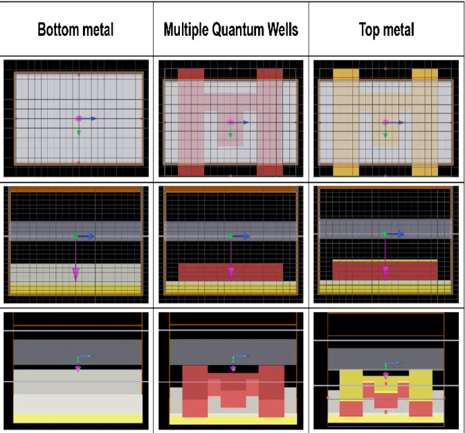
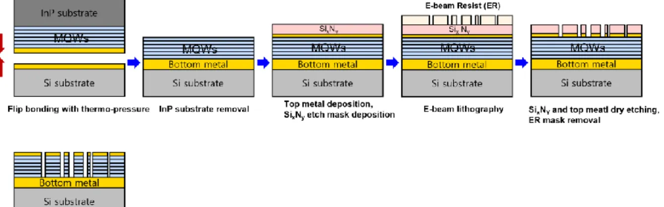
We did Flip bonding, wet etching, dry etching, electron beam lithography and deposition process to make DFG passive metasurface. With these passive fabrication steps, we fabricated the DFG passive metasurface which had no electrode. The dark layer at the bottom is the bottom metal which consists of Cr, Pt and Au.
For mesa patterning, the SixNy mask layer was deposited and the photoresist mask (PR mask) was spin-coated onto the sample. After photolithography (PL) with a size of 300 μm × 300 μm for protecting the array, the sample was dry etched to the bottom metal by ICP-RIE. Finally, before applying bias to the MQW, the top contact pad was deposited with Cr with a thickness of 20 nm, Cu with a thickness of 300 nm, Cr with a thickness of 10 nm, and Au with an electron beam evaporator.
We did wet etching, dry etching, photolithography and deposition process to make passive DFG metasurface. In Figure 3.4.4 (a), the purple layer is the bottom metal layer and the yellow T-shaped layer is a contact pad which can apply bias to the DFG metasurface. The large square is made by mesa etching and another is made by passivation pattern.
Experimental Results
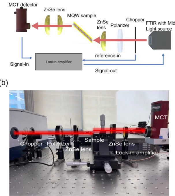
The light was detected by an MCT detector and the analog data is processed by a lock-in amplifier. From section 3.4, we fabricated the DFG metasurface by nanofabrication, such as flip-bonding, deposition, etching and others. The DFG metasurface was fabricated as a two-dimensional 100 μm by 100 μm array of the nanoresonator structure.
Using a 10.6 μm CO2 laser light source and a 6.1 μm to 6.9 μm QCL light source collimated in free space, a 14 μm to 20 μm irradiated wide range of difference frequency generation (DFG). in free space. Therefore, we fabricated the metasurface to meet the conditions and measured the reflectance spectra using FTIR. The passive DFG metasurface is designed to have strong absorption peak at 6, 10.6 and 14 μm (b) and (c) are experimental results of the reflectance spectra when the polarization of the incident light is (b) x- and (c) y- polarization.
The strong absorption peak was calculated near 6 μm wavelength in the incident x polarization of the incident light. On the other hand, in the case of y polarization, there were two absorption peaks at 10 μm and 14 μm wavelengths. After measuring the reflectance spectra of the passive DFG metasurface, we fabricated the active DFG metasurface as Figure 3.4.3.
One is connected to the contact pad which is connected to the top metal and the other to the bottom metal. A bias voltage of -4 V to +3 V was applied to the DFG metasurface with a step of +1 V and the x- and y-polarized reflection spectra were measured with an FTIR spectrometer. An external bias voltage was applied from −4 V to +3 V, and the light polarization is (a) x-polarization and (b) y-polarization.
Conclusion
Ultrafast quantum well photodetectors operating at 10 μm with a flat frequency response up to 70 GHz at room temperature.