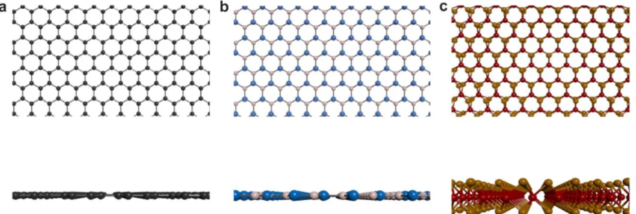
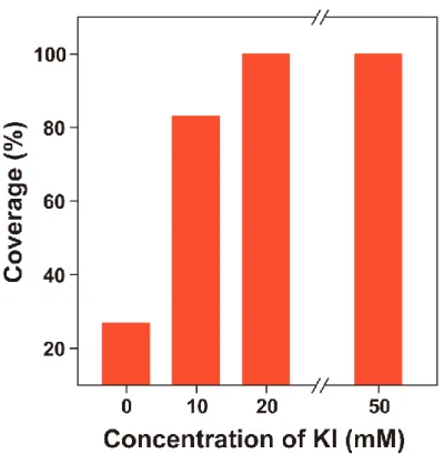
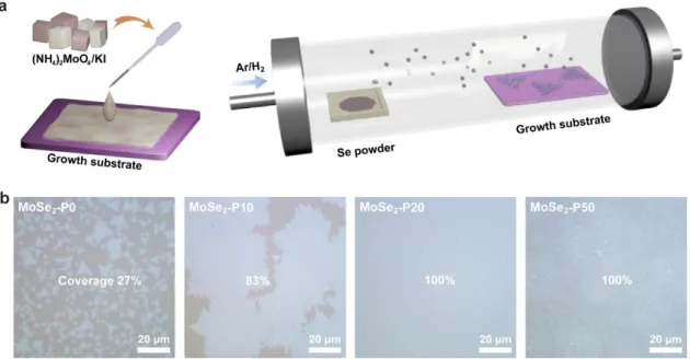
Summary of the field-effect mobility and current on/off ratio based on TMDs grown by liquid-phase precursor-based CVD in the literature. Synthesis of MoSe2 via promoter-assisted liquid phase CVD process. a) Schematic of the synthesis process for MoSe2 using liquid phase precursors. The coverage of MoSe2 on the growth substrate (sapphire) varies from 27% to 100% with increasing potassium iodide concentrations.
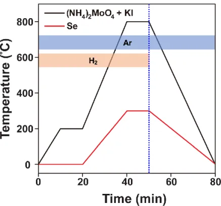
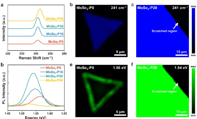
Temperature profiles of the promoter-assisted liquid-phase CVD process for the synthesis of MoSe2. AFM images and height profiles of (a) MoSe2-P0, (b) MoSe2-P10, (c) MoSe2-P20, and (d) MoSe2-P50 synthesized on sapphire substrate with different concentrations of potassium iodide. Spectroscopic characterizations of MoSe2 monolayer synthesized in different concentrations of potassium iodide. a) Raman spectra of MoSe2 with different growth promoter concentrations.
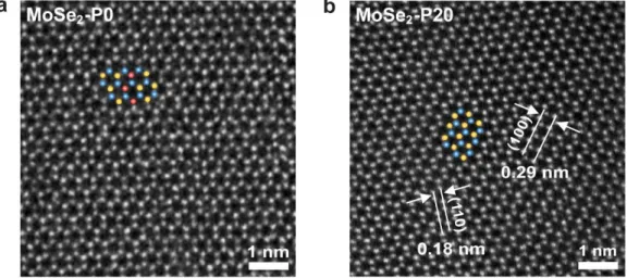
From the fitting, we achieved a binding energy of 24.8 meV for X−. Atomic structure analysis of MoSe2 monolayer grown at different concentrations of potassium iodide. a, b) STEM images of MoSe2-P0 and MoSe2-P20, respectively, showing the highly crystalline hexagonal structure of MoSe2-P20 with negligible selenium vacancies. Large-scale synthesis of MoSe2 monolayer film. a) Digital image of a uniform continuous large-scale MoSe2 layer synthesized on a 3 cm × 3 cm sapphire substrate. OM images of (a) MoS2, (b) WS2, and (c) WSe2 films synthesized on scratched sapphire substrates.
AFM images and height profiles of (a) MoS2, (b) WS2, and (c) WSe2 films synthesized via the promoter-assisted liquid-phase CVD process. a, b) Analysis of Raman and PL spectra of three types of monolayer TMDs films, showing the characteristic peaks for each corresponding TMDs.
Introduction
Synthesis of TMDs films via promoter-assisted liquid-phase CVD
Research background
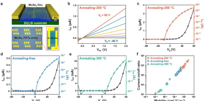
It can also reduce the energy barriers of the chalcogenization process at the edges.26-28 As a result, the uniform monolayer film of high-quality molybdenum diselenide (MoSe2) can be successfully synthesized on a 3 cm × 3 cm sapphire substrate. . Additionally, the electrical transport performance of the MoSe2 monolayer film was evaluated by fabricating field-effect transistors (FETs), achieving electron mobilities of up to 2.5 cm2 V−1 s−1 with an on/off ratio of up to 105. both of which are significantly higher than previously reported CVD-grown TMDs based on liquid-phase precursors. Our new strategy provides insight into wafer-scale uniform growth of high-quality monolayer TMD film and sheds light on their practical applications in electronics and optoelectronics.
Experimental section
A 532-nm continuous wave excitation laser was focused on the sample through a microscope objective lens (100×, NA = 0.7, Mitutoyo) and the PL signal was collected with the same lens. Then the signal was sent to a spectrometer (grating of 150 grooves/mm) with an InGaAs array CCD (Princeton Instrument) to obtain the desired spectra. Prior to device fabrication, the monolayer MoSe2 films were transferred onto a heavily doped, 300-nm-thick SiO2/Si substrate via the conventional poly(methyl methacrylate) (PMMA) assisted wet transfer method.
The PMMA support layer was removed with acetone and then annealed at 200 °C and 300 °C in an Ar atmosphere. MoSe2 FET devices were fabricated by standard photolithography, reactive ion etching (O2 100 sccm, 100 W, 20 s) and thermal evaporation of Cr/Au (5 nm/40 nm) source/drain electrodes. The thermal annealing treatment was further performed at 200 °C in a tube furnace for 1 h in an Ar atmosphere after depositing the source/drain electrodes.
The surface morphology of the TMD monolayers was characterized by optical microscopy (OM) (Eclipse LV150, Nikon) and AFM (DI-3100, Veeco). The Raman and PL spectra were acquired under ambient conditions using the Alpha300R spectrometer (WITec) with a laser excitation wavelength of 532 nm. The electrical properties of the films were measured in a vacuum (7 × 10⁻⁵ torr) at room temperature using a probe station (M6VC, MSTECH) with the Keithley SCS-4200 semiconductor parameter analyzer.
Synthesis of monolayer MoSe 2
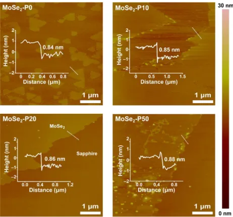
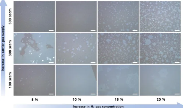
AFM images and height profiles of MoSe2 synthesized on the sapphire substrate with varying potassium iodide concentrations. The morphology of MoSe2 synthesized by promoter-assisted liquid-phase CVD technique was investigated at different hydrogen gas concentrations and the amount of carrier gas to determine the optimized synthesis conditions (Figure 2.5). The supply of hydrogen gas was known to promote the growth of TMDs in the CVD process, including MoSe2 WS2, and WSe2, by enhancing chemical reactivity between transition metal oxide and chalcogenides.
However, in the case of excessive supply of hydrogen gas, a decrease in TMD's domain size or unintended growth may be generated due to the hydrogen etching effect. Furthermore, the flow rate of carrier gas is essential for TMDs growth as it can modify the precursor vapor pressure. We introduced the total amount of carrier gas with 100, 300 and 500 sccm and increased the hydrogen ratio from 5 to 20% for each condition.
First, when 5% hydrogen was used in the total carrier gas of 100 sccm, a small flake size was observed, while a continuous MoSe2 film was formed as the amount of hydrogen increased. Moreover, it has been confirmed that multilayer MoSe2 flakes exist on a continuous film under high hydrogen gas concentration conditions (15 and 20%). At the lowest concentration of hydrogen gas (5%), too little hydrogen gas was supplied to insufficiently promote the evaporation of the precursor.
The synthesis of MoSe2 was therefore rare, resulting in the formation of very small flakes in some parts. At the high hydrogen gas concentration, the chalcogen precursor evaporated rapidly to promote selenization, forming a continuous layer with an additional layer on the film, similar to excessive treatment with potassium iodide (MoSe2-P50). Secondly, we analyzed the influence of the total amount of carrier gas on the growth of TMDs by controlling the delivered rate of carrier gas under the CVD condition.
When the hydrogen concentration was fixed at 10, 15, and 20% while the amount of carrier gas increased to 300 and 500 sccm, the floc size gradually decreased while the nucleation density increased significantly. This suggests that the etching effect occurred as the absolute amount of hydrogen gas increased. We therefore determined the optimal CVD condition for synthesizing a uniform monolayer MoSe2 continuous film with negligible few-layer areas at a hydrogen gas concentration of 10% with a total carrier gas of 100 sccm.
Characterization analysis of monolayer MoSe 2
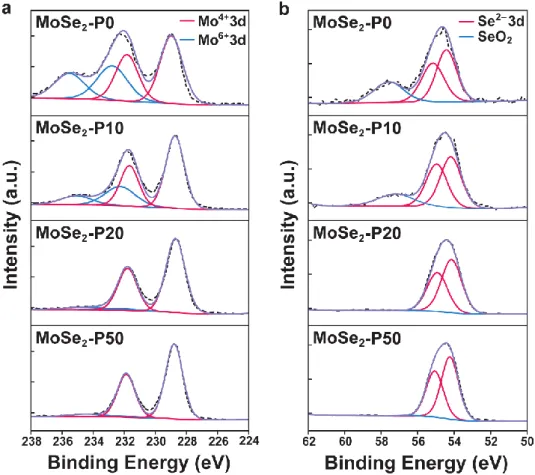
In addition, the oxidation state, SeO2 peak, was analyzed to investigate the quality of MoSe2 and showed similar behavior to the Mo6+ peak (Figure 2.6b). We investigated the quality of MoSe2 samples grown with different concentrations of potassium iodide through Raman and PL spectroscopy. The typical Raman spectrum of MoSe2 in Figure 2.7a shows the characteristic peak, which is the A1g phonon mode (out-of-plane vibrational mode).
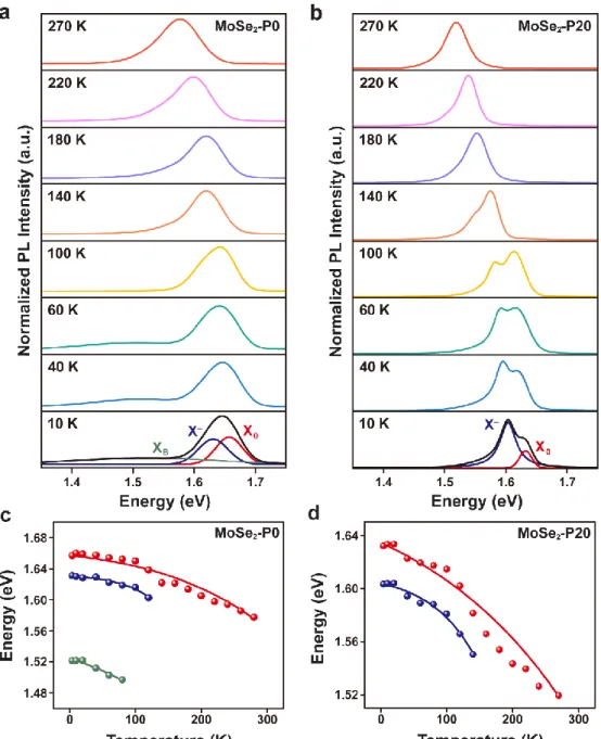
It is known that the n-doping effect of monolayer TMDs caused by the chalcogen vacancy causes the Raman intensity to decrease due to the softening of A1g. The PL intensity rapidly decayed from the boundary to the middle region of MoSe2. Temperature-dependent PL analysis was performed with temperature decreased from 270 to 10 K to identify whether the optimal concentration of potassium iodide (MoSe2-P20) promotes excitonic emission and suppresses defect-related emission.
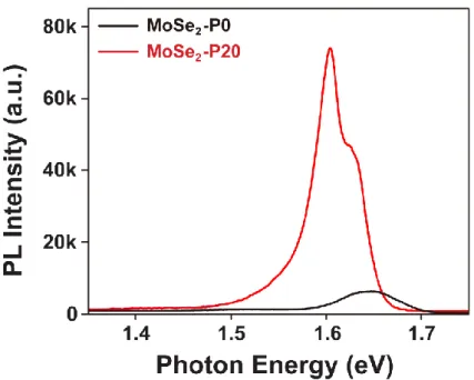
In addition, the difference in binding energy between the X0 and X− peaks shows 30 meV, indicating the intrinsic emission of the MoSe2 exciton. The temperature dependence of the position of the peaks X0, X− and XB, which is extracted from Figure 2.8a, b, is shown in Figure 2.8c, d. Therefore, the observed temperature-dependent optical characteristics of MoSe2 grown by the liquid-phase CVD technique, including high brightness, narrow linewidth, and reduced defect-related emission, contributed to the improvement of the crystalline quality of MoSe2 at the optimal potassium iodide concentration. a, b) Temperature-dependent PL spectra of MoSe2-P0 and MoSe2-P20, respectively. MoSe2-P20 shows a strong PL intensity and a narrow linewidth compared to MoSe2-P0, indicating that the quality of the MoSe2 crystals was improved by the potassium iodide treatment.
In STEM images, the brightness of atoms is directly related to atomic number. Thus, the regions of the Se atom (Z = 34) where the overlap of two Se atoms is observed are relatively brighter than the regions of the Mo atom (Z = 42).38 As shown in Figure 2.11a, some Se vacancies (red spheres ) are in some regions, although the hexagonal crystal structure of MoSe2 clearly appeared in the MoSe2 lattice without potassium iodide. Meanwhile, we note that the lattice spacing of 0.29 and 0.17 nm assigned to the (100) and (110) planes of hexagonal crystal structures is defect-free in the STEM image of MoSe2-P20 samples and demonstrates that the monolayer film of high was MoS. achieved (Figure 2.11b).
In addition, the SAED pattern of MoSe2-P20 clearly shows the hexagonal diffraction pattern in Figure 2.12. As shown in Figure 2.13, EDS analysis was also performed to determine the elemental composition of the MoSe2 (MoSe2-P20) monolayer film based on the white box region shown in the left figure. The Se/Mo atomic ratio for MoSe2 was calculated to be 1.94 (Table 2.1), indicating the successful formation of MoSe2 with negligible Se vacancies (Figure 2.13).
Large-scale growth of monolayer MoSe 2
To obtain information about the lattice structure of monolayer MoSe2, STEM was performed on MoSe2-P0 and MoSe2-P20 samples. Atomic structure analysis of monolayer MoSe2 grown at different concentrations of potassium iodide. a, b) STEM images of MoSe2-P0 and MoSe2-P20, respectively, showing a highly crystalline hexagonal structure of MoSe2-P20 with negligible selenium vacancies. EDS spectrum of monolayer MoSe2 film measured from the white boxed areas in the left TEM image.
The Se/Mo atomic ratio of MoSe2 was calculated to be 1.94, confirming the successful formation of MoSe2 with negligible Se vacancies.
Electrical properties of monolayer MoSe 2
Universality of the promoter-assisted liquid-phase CVD
The inset shows the OM image of MoSe2 devices with a channel length of 25 μm (scale bar: 10 μm).
Conclusions
Ultrasensitive surface plasmon-free enhanced Raman spectroscopy with femtomolar detection limit from 2D van der Waals heterostructures. Many-body simulation of two-dimensional electron spectroscopy of excitons and trions in single-layer transition metal dichalcogenides. Wafer-scale synthesis of thickness-controllable MoS2 films via solution processing using a dimethylformamide/n-butylamine/2-aminoethanol solvent system.