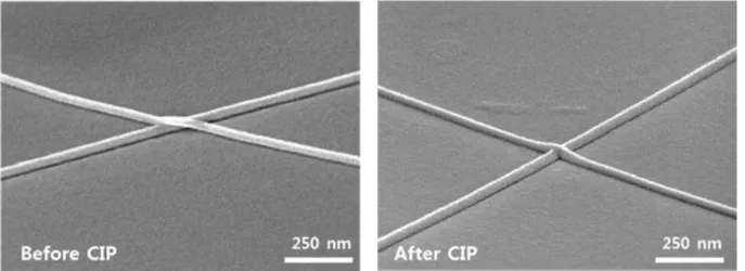
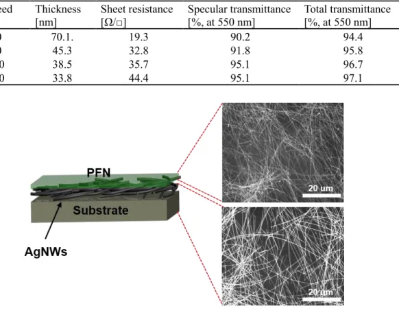
Inset shows an optical image of the PET/ITO film after bending with a radius of 4.5 mm. Differences in the optical transmission of the CIP-treated AgNW electrodes formed under different spin speeds.
Introduction
- Solar Energy
- Photovoltaic Devices
- Flexible Photovoltaic Devices
- Understanding of Photovoltaic Devices
- Organic Solar Cells (OSCs)
- Issue of OSCs
- Flexible OSCs
- Interlayer
- Transparent Electrodes
- Inorganic-Organic Hybrid Perovskite Solar Cells (IOHP)
- Objective and Scopes
The current-voltage curve of the solar cell can be added together with the diode current-voltage curve and the photogeneration current in the dark state. In this case, the ratio of the light energy incident on the unit area to the output of the solar cell is defined as η.

Background and Literature Survey
History of OSCs
Physics of OSCs
- Principle of OSCs
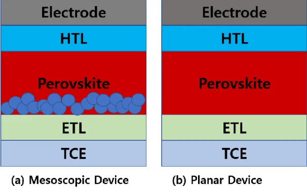
- Structure of OSCs
This structure is unique to the OSCs and differs from the p-n junction structure of the primary inorganic solar cell. If the thickness of the photoactive layer is thin, it obviously cannot completely absorb the light.

Electron Transport Materials (ETMs)
- Metal Oxide
- Polymer Electrolyte
As mentioned earlier, the thickness of the photoactive layer of the OSCs is about 100 nm, which is the thinnest structure of all solar cells currently called "nano-solar cell". For this reason, it can affect all solar cell elements, from FF to VOC, even JSC, of the solar cell.27 In the Y.
Transparent Conducting Materials (TCMs)
- Polymer based Materials
- Carbon based Materials
- Metal based Materials
Thus, it was evaluated as an active ETL capable of not only transporting electrons to the cathode but also acting as an ejector. Carbon nanotubes (CNTs) and graphene, which are produced by applying carbon, have relatively low conductivity compared to metal electrodes, but have excellent flexibility and transparency.29 Recently, many efforts have been made to increase the conductivity of this carbon-based electrodes using chemical treatment techniques or by forming hybrid structures with other transparent conductive materials. Since the physical flexibility and transparency of CNTs have been discovered, various studies have been conducted on the next generation of TCE.
Attracting attention as a next-generation transparent electrode in optoelectronics, graphene is a material suitable for flexible devices due to its excellent intrinsic mobility, Young's modulus, and high thermal conductivity.30 So far, various methods of graphene growth, such as chemical vapor deposition and epitaxial deposition, have been studied growth and studied useful devices. Therefore, CNTs, graphene, metal mesh, and AgNWs during TCE have been confirmed to maintain stable mechanical and electrical properties due to deformation, such as bending property, and have been intensively studied. However, since the fabrication is based on a semiconductor processing system such as patterning, deposition, and etching, it has the disadvantages of high manufacturing cost and process time.
Perovskite Solar Cells
- Perovskite Light Absorbing Material
- Device Structure and Working Principle
- Solvent Engineering in Perovskite Solar Cells
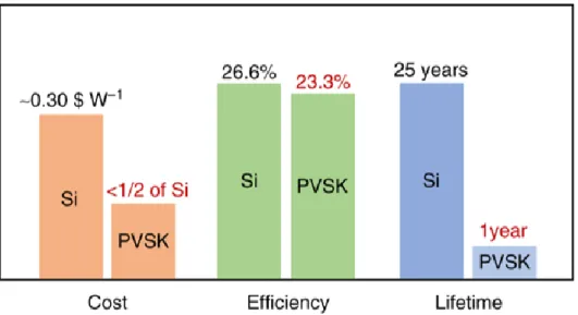
More than 90% of the current market for commercialized solar cells is occupied by crystalline silicon solar cells. Since then, research on the physical properties of IOHP materials has progressed, and the structure of the solar cells has gradually changed. From this point of view, the development history of PCE of perovskite solar cells can be considered as a history of film formation control technology of IOHP materials.
Subsequently, a technique for coating the perovskite solution with an additive has been reported as a method of controlling the density and uniformity of the perovskite thin film formed by such a single solution coating process.37,38 The additive retarded the crystallization during the formation of the perovskite thin film, and a relatively uniform thin film was obtained. A solvent engineering method was then used to produce a more uniform, planar and dense perovskite thin film.41 This process led to the formation of the intermediate phase by adding toluene as an anti-solvent to the spincasting step of the perovskite solution. Above, several technologies have been introduced and efforts are underway to develop the high PCEs of the perovskite solar cells through the low-temperature solution process.
Introduction
The technology using this low-temperature process is expected to be applied not only to electronic paper, which has been shown to be an essential material for next-generation displays, but also to technologies such as tandem structure that aim for high PCE.
Experimental
- Fabrication of IOSCs
- Bending Test
- Characterization
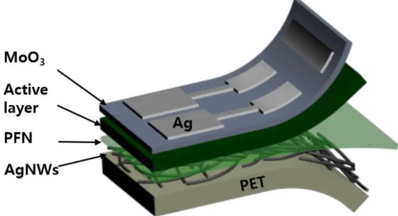
The AgNWs dispersion (Nanopyxis lnc.) was formed into a film by a spin-coating process with a speed range of 600–1200 rpm for 40 seconds. For subsequent ETL formation, the PFN interlayer material is formed to a thickness of less than 10 nm by a spin coating process. MoO3 (7 nm) and Ag (100 nm) with shadow mask are deposited on top of the device by thermal evaporation method.
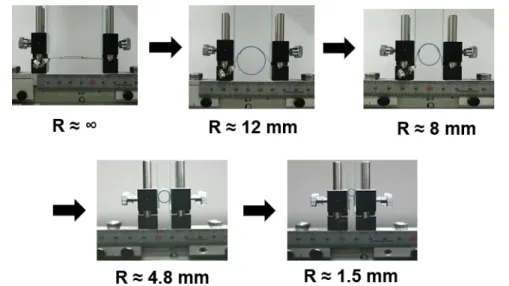
It was used to evaluate the resistance properties of the excellent radii of PET/ITO and PET/AgNWs/ZnO and PET/AgNWs/PFN films. It was also used to evaluate the performance characteristics of the fabricated flexible devices (PET/ITO, PET/AgNWs/PFN) after bending tests. The characterization of the IOSCs was performed in a nitrogen-filled glove box with simulated AM 1.5 illumination with light irradiance of 100 mW cm-2 using a high-quality optical fiber connected to a xenon arc lamp.
Optoelectrical Characterization of Interface Engineering using PFN Thin Film on Silver
- Optical and Electrical Measurement of PFN/AgNWs electrode
- Ultraviolet photoelectron spectroscopy (UPS) measurement
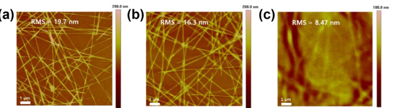
In Figure 3.6, AgNW films with a rougher surface than flat commercial ITO films showed a roughness reduction of 4 nm by coating the PFN layer, and the roughness of the surface covered with ZnO layer on AgNWs was also confirmed. For a better study of PFN/AgNWs in the solution process, the flexible IOSCs were fabricated using photoactive materials;. I first collected information about the work functions of AgNWs, ZnO/AgNWs and PFN/AgNWs films through UPS measurements in Figure 3.7.
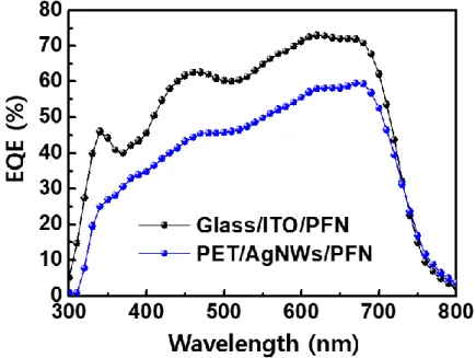
The binding energy of the secondary electron cutoff and the Fermi level measured from the injected energy (21.22 eV in our experiment) can be calculated using the following formula (φm = hν-(EF-ESC)). It can be concluded that PFN/AgNWs induce electron transport and electron collection with more effective energy matching at the LUMO level of PC71BM, the acceptor material for. The reason for this is that the PFN interlayer is located on the surface of the AgNWs, and the work function can be activated by charge matching from the photoactive due to the permanent interface dipole formation.
Photovoltaic Performance
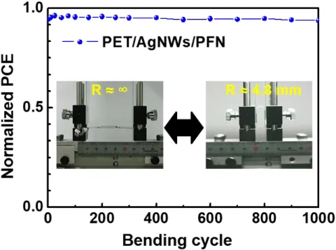
Measured changes in the resistances of the electrodes based on ITO/PET and PFN/AgNWs/PET films as a function of the bending radius. In Figure 3.12, the different characteristics of the AgNWs-based IOSC are compared with the ITO-based COSC at different bending radii. The excellent bending stability of the IOSC based on PFN/AgNWs allows the original VF to be maintained.
Like FF, the JSC of the ITO-based COSC is inversely proportional to the change in the bending radius and shows a reduction of about 34% at R 1.5 mm compared to the initial value. Conversely, the RDK of the PFN/AgNWs-based IOSC does not change up to bending radius R 4.8 mm, but only 7% at R 1.5 mm compared to the initial value. The VOC of the IOSC is not significantly affected by the bending radius, as shown in Figure 3.12 (c).

Conclusion
Transparent Conducting Electrode (TCE): Rational Design of AgNWs Cathode for
- Introduction
- Experimental
- Preparation of Cold-Isostatic Pressing (CIP)-AgNW Electrodes
- Preparation of ZnO nanoparticles
- Fabrication of flexible IOSCs and Characterization
- Observation of AgNWs Fabricated by CIP using an Electron Microscope
- Photovoltaic Performance
- Conclusion
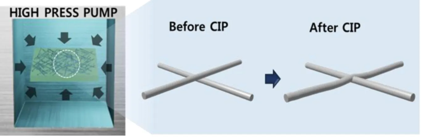
The shapes of the untreated AgNWs and CIP-treated AgNWs were measured by SEM (Hitachi S-4800), AFM (Veeco microscope), and transmission electron microscope (TEM, Cs-corrected STEM, 300kV). As shown in Figure 4.12, the surface roughness of the untreated AgNWs electrode formed on the PET substrate is generally large-scale in the flexible device structure, so the two electrodes (cathode and anode) of the device are often connected together. The untreated electrode has a root mean square (RMS) surface roughness of 42 nm, but the surface roughness of the CIP electrode is 26.7 nm (Figure 4.13).
In Figure 4.16, the current-voltage curves of the electrodes were measured to compare the electrical characteristics of the AgNW electrodes (untreated, annealed and CIP treated). This indicates that the internal resistance of the CIP electrode is the lowest among the electrodes to be compared. And the thermally annealed AgNWs have a higher resistance than the CIP electrode because the surface of the NWs can be oxidized during the thermal treatment.
To demonstrate the applicability of the CIP electrodes in flexible IOSCs, the devices were fabricated on flexible PET substrates. This slight reduction in the JSC and FF values will be caused by imperfections in the mechanical stability of the AgNWs electrode.
Solvent Additive Engineering in Perovskite Solar Cells: The Solvent-Coordination
- Introduction
- Experimental
- Preparation of Tin dioxide (SnO 2 ) film
- Solar cell fabrication and Characterization
- Thin Film Formation through Interaction of Perovskite Precursor with Solvent
- Photovoltaic Performance
- Conclusion
In addition, the photoluminescence (PL) analysis was used to determine the photovoltaic properties of the perovskite films. The reduction of charge recombination contributes to the improvement of the electrical performance of the perovskite solar cells. The perovskite solar cells with the respective solvent additives showed Voc, FF and PCE of the same trend as the grain size.
As the DN of the additive increases, it forms a strong complex with PbI2 and affects the grain size of the perovskite film. Various analyzes have shown that the optical and electrical properties of the perovskite film improve with increasing grain size. Finally, the PCE of the perovskite solar cell with DMS was achieved by 21.2% by improving each parameter.

Summary
Journal Permission
Ji Hoon Seo†, Inchan Hwang†, Han-Don Um, Sojeong Lee, Kangmin Lee, Jeonghwan Park, Hyeonoh Shin, Tae-Hyuk Kwon, Seok Ju Kang*, and Kwanyong Seo*, “Cold Isostatic Pressure Silver Nanowire Electrodes for Flexible organic solar cells with room temperature processes”, Advanced Materials. Seung Yoon Ryu†*, Ji Hoon Seo†, Hassan Hafeez†, Myungkwan Song, Jun Young Shin, Dong Hyun Kim, Yong Chan Jung, and Chang Su Kim*, "Effects of Wrinkle Structure and Flat Structure Formed During Static Low Temperature Annealing ZnO in the performance of inverted polymer solar cells", The Journal of Physical Chemistry C. Seung Yoon Ryu†*, Ji Hoon Seo†, Hassan Hafeez†, Myungkwan Song, Jun Young Shin, Dong Hyun Kim, Yong Chan Jung , Chang Su Kim* , “Improved hydrogenated amorphous silicon thin-film solar cells created by replacing the n-type Si layer with a PFN interfacial layer,” Synthetic Metals.
Hyun-Tak Kim†, Ji Hoon Seo†, Jeong Hyuk Ahn†, Myung-Jin Baek, Han-Don Um, Sojeong Lee, Deok-Ho Roh, Jun-Ho Yum, Tae Joo Shin, Kwanyong Seo* and Tae-Hyuk Kwon*, “Tailored energy reduction using iridium complexes for improved performance of polymer solar cells,” ACS Energy Letters. Ji Hoon Seo†, Han-Don Um†, Atul Shukla, Inchan Hwang, Juyun Park, Yong-Cheol Kang, Chang Su Kim, Myungkwan Song*, and Kwanyong Seo*, “Flexible organic solar cells processed by low-temperature PFN/AgNWs cathode”, Nano energy.
Acknowledgement