The use of surface plasmon resonance (SPR) effects of metallic nanostructures is one of the most promising approaches for improving the performance of organic optoelectronic devices. Note that G', C' and S' have the same morphologies, but reverse polymer components of the G, C and S systems. The molecular weight of the block copolymer determines the size of the microdomains, typically _10 nm.
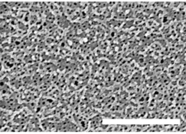
The inset in (b) shows a field emission electron micrograph of the film showing the uniformity of the pore size.
List of Tables
Introduction
- History of Organic Optoelectronics
- Physics of Organic Optoelectronics
Jsc is the current density of solar cells when the output voltage of solar cells is zero. Voc is the maximum voltage of the solar system when the solar cells are operating at an open circuit with zero current. Rλ is defined as the ratio of the generated photocurrent (Ip) to the incident light power (P) at a given wavelength in units of amps/Watt.
In other words, Rλ is the efficiency of the light power conversion to an electric current and is the preferred measure of a photodiode's response to light. Where h is the Planck constant, c is the speed of light, q is the electron charge, Rλ is the responsivity in A/W and λ is the wavelength in nm. NEP is the incident light power of the photodiode, which generates the same photocurrent as the noise current.
Ion is defined as the maximum current of the transfer curve and Ioff is defined. Vth is defined as the x-intercept of the extension line of the square root of the drain current.8 The extension line is determined near the on-current.

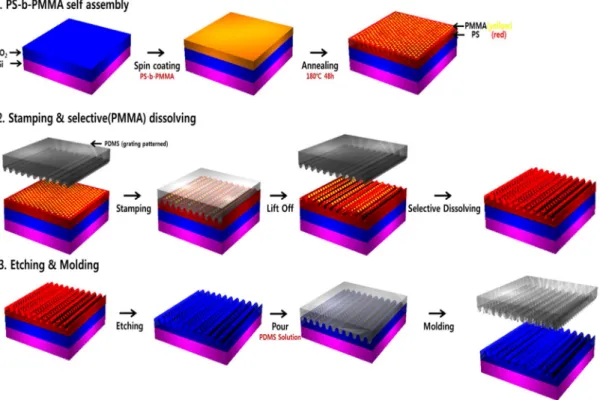
Fabrication of Dual Patterned Si wafer and PDMS mold for Plasmonic Effect 3.1 Experimental
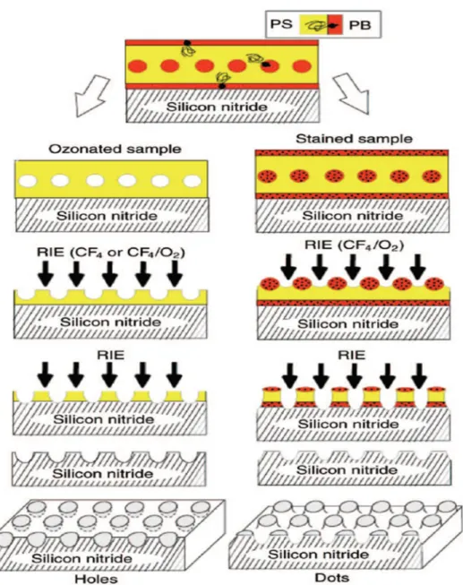
To fabricate a double-pattern SiO2 mold with a PDMS stamp, the PDMS stamp was placed in conformal contact with the PS-b-PMMA and then stamped at 130 ℃ with a pressure of 35,000 pa for 10 minutes. After removing the PDMS mold, PMMA was selectively etched with the traditional UV/acetic acid treatment to create double-patterned PS film. Then, an inductively coupled plasma etching (ICP) process was performed to etch the SiO2 layer using a double-patterned PS cartridge as a mask.
After the etching process, the double-patterned SiO2 wafer was treated with UV ozone and treated with fluorine for 20 minutes. After baking at 60 ℃ for 2 hours, the solidified double-patterned PDMS lattice mold could be easily stripped. It is clearly shown that double-patterned PS film consists of lattice pattern and random nanohole patterns.
The dual-patterned SiO2 was fabricated by inductively coupled plasma (ICP) etching using dual-patterned PS film as a mask. The PS film with double pattern, bright nanoholes and lattice pattern could be fabricated on a large scale, as shown in Figure 3.6. Optical image of double-patterned PS films, of which NIL has been partially performed, is also shown in the figure.
We can observe that double-patterned PS film clearly shows different colors according to the camera angles, caused by the interface effect with the grating pattern. Importantly, our approach realizes a dual pattern that does not change the nano-holes and lattice pattern of the PS film. In addition, to fabricate other double-patterned organic films of NIL, we have obtained a double-patterned PDMS stamp through a traditional PDMS casting process by using a double-patterned SiO2 layer as the main mold.
After selectively dissolving PMMA, we used a double-patterned PS film as a mask during an inductively coupled plasma etching process and prepared a bright double-patterned SiO2 layer. Furthermore, we prepared a double-patterned PDMS stamp based on a double-patterned SiO2 layer as a mold. The dual-patterned SiO2 layer and PMDS stamp can be used as a promising substrate and stamp for optoelectronics, respectively.
Chapter 4. Surface plasmon resonance of dual patterned gold back reflector electrode
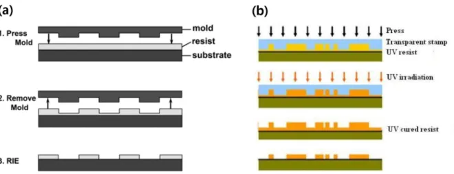
In this work, we used a vacuum-assisted NIL to produce the active layer pattern without heating. For comparison, AFM images and the heights of the planar, lattice and double-pattern active layers are also shown in the figure. Compared with the lattice-patterned active layer, the lattice-patterned nanoholes and cones are clearly observed in the AFM image of the double-patterned active layer.
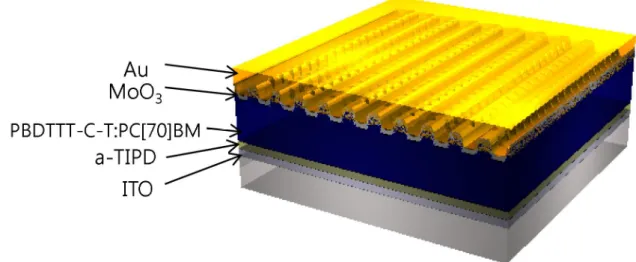
The improvement of Jsc from the double pattern was more than double that of the lattice pattern. In addition, the intensity of IPCE enhancement of the Au-dual pattern OPVs was much higher than that of Au-grating-only OPVs. Furthermore, the absorption characteristics of different active layer patterns with Au (30 nm thickness) (Figure 4.5a) and without Au (Figure 4.5b) showed the role of the Au pattern.
It shows that the characteristics of the double-patterned active layer and the grating-patterned active layer exhibit similar characteristics. The absorption data of the active layer with an Au electrode thickness of 30 nm, which clearly shows the intensity enhancement, is shown in Figure 4.5b. The electric field contour plots of the flat model (Figure 4.7a), the lattice model (Figure 4.7b), and the double pattern effect model (Figure 4.7c) are also shown.
In contrast to the electric field of the flat model, the lattice model showed high enhancement at the interface between Au and PBDTTT-C-T:PC[70]BM. This means that the lattice pattern increases the electric field intensity of the interface and improves the extinction spectra for the efficiency of OPVs. Based on equations (1)-(3), we calculated R, SNR, and the EQE values of the photodiodes based on the non-pattern, lattice pattern, and dual pattern at 1 V bias, as shown in figure 5.4.
We calculated the extinction spectra for flat and lattice models (Figure 5.5a) and double pattern effect models (Figure 5.5b). In Figure 5.5a, the grating shows slightly improved extinction spectra at a wide wavelength range (450 ~ 900nm). Electric field contour plots of the flat model (Figure 5.6a), lattice model (Figure 5.6b) and double pattern effect model (Figure 5.6c) are also shown.
The electric field of the lattice pattern, compared to the flat pattern, showed high enhancement at the interface between Al and P3HT:PC[60]BM. Also, the electric field of the double pattern effect pattern showed strong improvements at the pattern interfaces.
Chapter 6. Surface plasmon resonance of dual patterned gold back reflector electrode
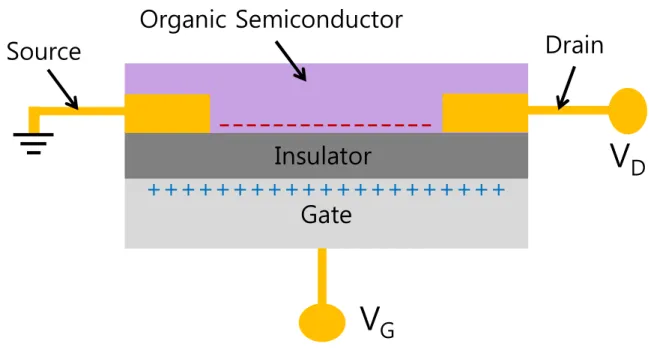
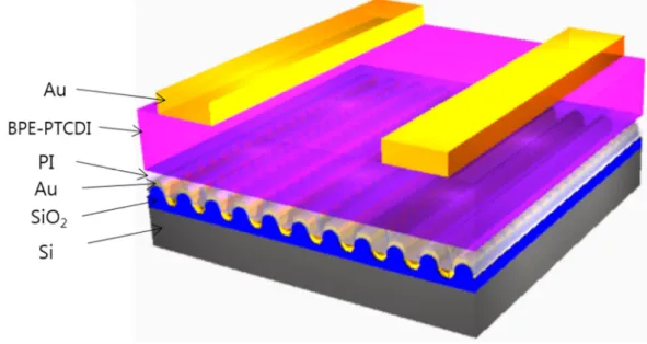
To exploit the plasmonic effect, we used a transparent polyimide dielectric layer with a capacity of 7 μF/cm-2. In addition, to prevent damage to the dielectric layer during the dissolution process of the semiconductor layer, N,N′-bis(2-phenylethyl)perylene-3,4:9,10- tetracarboxylic diimide (BPE-PTCDI), which is a promising N-type semiconductor, was thermally deposited. Furthermore, under green light, the EQE of dual-pattern OPTs increased dramatically from 1.61 (flat OPTs) to 17.8 (grating OPTs).
All lines and lower located lines located in the upper and lower parts of the graphs refer to photoswitching with 100 V gate bias (closed circles) and 0 V gate bias (open circles), respectively. Therefore, improvement of the photoswitching ratio using a dual pattern varied with R, EQE and SNR of the transfer curve. Therefore, we can predict why the EQE of the grating was lower than the flat model at 670nm through extinction enhancement.
We hypothesized that NWs increase the mobility of charge carriers to reach the transistor accumulation layer due to the high mobility of NWs. Changing the electrode pattern leads to improved electric field distribution, causing significant changes in light absorption and scattering within the device architecture. In the flat model, the size of the active layer is 300nmⅹ1nm in length at the bottom and 100nm in height.
In the photovoltaic structure, the active layer material is PBDTTT-C-T:PC[70]BM. 80nm gold (Au) is coated on this layer. In the photodiode structure, the material of the active layer is P3HT:PC[60]BM., aluminum (Al) with a thickness of 100 nm is coated on this layer. Figures 7.1c and 7.1d show the planar and grating pattern unit patterns, respectively, used in the phototransistor structure.
In the flat model, the size of the active layer is 300nmⅹ1nm bottom length and 40nm height. In the grating pattern model, the size of the active layer is 300nmⅹ1nm at the bottom length and a 20nm grating height. The depth of the double pattern is 4nm, which is the maximum depth in the experiment measurement.
These significant improvements in device efficiency demonstrate that dual-pattern plasmonic effects constitute a versatile and effective route for achieving high-performance OPVs, OPDs, and OPTs. In addition, increasing the surface area of the dual pattern also has the potential to be used as a route to improve the performance of chemical signal sensing.
Acknowledgements
감사의 글