저작자표시-비영리-변경금지 2.0 대한민국 이용자는 아래의 조건을 따르는 경우에 한하여 자유롭게
l 이 저작물을 복제, 배포, 전송, 전시, 공연 및 방송할 수 있습니다. 다음과 같은 조건을 따라야 합니다:
l 귀하는, 이 저작물의 재이용이나 배포의 경우, 이 저작물에 적용된 이용허락조건 을 명확하게 나타내어야 합니다.
l 저작권자로부터 별도의 허가를 받으면 이러한 조건들은 적용되지 않습니다.
저작권법에 따른 이용자의 권리는 위의 내용에 의하여 영향을 받지 않습니다. 이것은 이용허락규약(Legal Code)을 이해하기 쉽게 요약한 것입니다.
Disclaimer
저작자표시. 귀하는 원저작자를 표시하여야 합니다.
비영리. 귀하는 이 저작물을 영리 목적으로 이용할 수 없습니다.
변경금지. 귀하는 이 저작물을 개작, 변형 또는 가공할 수 없습니다.
Master's Thesis
Gayoung Kim
School of Energy and Chemical Engineering (Energy Engineering)
Ulsan National Institute of Science and Technology
2022
Highly reliable and uniform carbon nanotubes
transistors for biosensor application
2022
Gayoung Kim
School of Energy and Chemical Engineering (Energy Engineering)
Ulsan National Institute of Science and Technology
Highly reliable and uniform carbon nanotubes
transistors for biosensor applications
IjITI)gUnqΛ
Ⅱ
Ir
Kq
Λ pΘ oJdd∀
Ⅱ
OISSIIIIqnS JO ZZOZ˙
ι
90 0˙
IIIIΣ
BunoΛ
D
ℓΘ
ouΘIos Jo JΘ 'Sℓ
ν
' UIΘ θ S'Ⅱ JOJ II) θ P JBΘ Θ Θ JO
JInboJ
oIIIJO
Θ 'Ⅱ UIIIIJI삥
IΨ Iℓ
η
d UI
KBololrㅐ
ㅗ oΘ
ooIToIoS puℓ
어 η JO
I)SⅡ I
Ⅱ Iℓ OI1ℓN
SIn IIℓ
어
Pθ
”
qns IⅢ IIolwμ
Θ
sslp/slSΘ II' V
sⅡ
woIIddℓ
oτqn↓
sΘu 0uℓ uoqJℓo
JosuΘ solq JoJ
UIJOJTLIn PⅡ
ℓ sJolsτ
jη
suℓ
Iqℓ
Θ
J
TIΘBIH KI니
nKBo∃ uIIτ
η τ 乏 4ι
'
Ⅱ
OISSIIIIqnS JO
˙ ι ZZOZ
˙ 0
90
˙ Λ pΘ
oJddℓ SI IIII) BUnqÅ
Ir Ⅱ
Jo
1ℓ uoτ yΘsslp/slsΘ II'
oII' II' 1ℓ TJIΨ SΘ
Θ
o SIH』L
u"∑
BunoΛ
D
ℓsuol'ℓ oIIdd●
Josu3solq JoJ SJ어
STSUℓ
쨔
q㎁ㅠ oΣ
nAH
Ⅱq'10uℓ
sΘu uoqlℓo
uIJoJTun
Θ puℓ
Iqℓ
J
IIΘBIH KI니
Abstract
SWNTs have excellent mechanical, electrical, and thermal properties, which distinguishes them from other device materials. Therefore, they are being actively studied in various electrical device fields. In particular, the small sizes as nanostructure, large surface area-to-volume ratio and their chemical functionalization allow the high-sensitivity signal conversion, which is an attractive factor in biosensors.
However, to use the superior properties of SWNTs for research, it is necessary to solve the problems of bundling by van der Waals force and mixed electrical properties. These problem can be overcome as sc-SWNTs could be simultaneously separated and dispersed by the interaction between π electrons of the carbon nanotubes and the conjugated polymers. SWNTs FETs fabricated by these sorted sc-SWNTs are expected to their potential because of their high carrier mobility and excellent electrostatic properties.
But, SWNTs FETs with great performances exceeding that of conventional MOS-FETs haven’t yet been realized at technologies node due to several problems with SWNTs materials. For the ideal SWNTs FETs, the film stability and long-time of fabrication by most physical adsorption methods must be solved. It is also necessary to find an appropriate density of SWNTs layers on designated active region to achieve high and uniform performance. Similarly, in a biosensor having frequent washing processes, the intrinsic electrical properties of SWNTs films fluctuated due to the unstable anchoring of SWNTs on the platform surfaces after several washing steps of biosensors, so SWNTs film stability with substrates must be ensured.
In order to solve these problems and utilize the SWNTs, a chemical immobilization method of SWNTs on a substrate with wrapping polymer that can form chemical bonds between sc-SWNTs and adhesive layer is proposed. Azide-functionalized polyfluorene derivatives were synthesized as wrapping polymers, and only sc-SWNTs were selectively enriched by this polymers. Then, the alkyne functionalized polymer was synthesized for Click reaction, and successfully patterned by UV light attachment. Sorted sc-SWNTs solution of low concentration was reacted with alkyne adhesive layer of the substrate by Click reaction to achieve a dense and firmly immobilized SWNTs pattern networks in a short time. Patterned SWNTs films, which form strong bonds with the substrate even after the sonication washing, can be obtained through a simple adhesive layer pre-patterning without a photoresist process. By minimizing the interference and leakage current between devices, the patterned SWNTs FETs have excellent performance and homogeneity compared to the un-patterned FETs because the device is manufactured by accurately dividing the channel region.
Then, to apply this patterned SWNTs FETs as biosensors, a linker and an antibody were immobilized on the SWNTs films, and Alzheimer's antigen was detected by confirming the change of the electrical
resistance response. The resistance value of SWNTs FETs showed almost the same value without change even after the sonication washing by PBS solution. This means that the SWNTs film is still bonded to the substrate by the Click reaction even after the harsh washing process, which solves the problem of film exfoliation of common SWNTs biosensor platform. In Aβ1-42 peptides detection, a significant increase in resistance was identified only when the antibodies were immobilized to the devices. This result shows that the patterned SWNTs devices fabricated by Click reaction can be successfully applied as biosensor platforms with specificity to target materials.
i
Contents
Contents ···ⅰ
Contents of Figure ··· iii
Contents of scheme ··· v
Contents of Table ··· vi
Nomenclatures ··· vii
Ⅰ. Introduction ··· 1
1.1. Backgrounds of carbon-nanotubes ··· 1
1.2. Structures and electrical properties of carbon-nanotubes ··· 4
1.3. Purification method of selective dispersion by conjugated polymers ··· 7
1.4. Single-walled carbon nanotubes field effect transistors ··· 12
1.5. Electrochemical biosensors based on carbon-nanotubes ··· 14
1.6. Motivations ··· 15
Ⅱ. Experimental Methods & Materials ··· 16
2.1. Materials and Characterization ··· 16
2.2. Materials Synthesis ··· 16
2.2.1. Synthesis of 4-(Allyloxy)benzophenone, ABP ··· 16
2.2.2. Synthesis of 4-(3’-Chlorodimethylsilyl) –(propyloxy)benzophenone, BPS ··· 16
2.2.3. Synthesis of 5-acryloyloxyisophthalic acid, APA ··· 18
2.2.4. Synthesis of Di(propargyl)-5-(Acryloxyloxy)isophthalate, DPAP ··· 19
2.2.5. Synthesis of poly(dipropargyl-5-(acryloyloxy)isophthalate-r-propargylacrylate, P(DPAP-r-PA) ··· 22
2.2.6. Synthesis of 2,7-dibromo-9,9-bis(12-bromododecyl)9H-fluorene, FD-Br ··· 23
2.2.7. Synthesis of 2,7-dibromo-9,9-bis(12-azidododecyl)9H-fluorene, FD-N3 ··· 25
2.2.8. Synthesis of 2,2'-(9,9-didodecyl-9H-fluorene-2,7-diyl) bis(4,4,5,5-tetramethyl-1,3,2-dioxaborolane), FD-pinacolborane ··· 27
2.2.9. Synthesis of poly(didodecylfluorene-alt-bis-azidododecyl-fluorene), P(FD-N3) ··· 29
2.3. Enrichment of the selectively sc-SWNTs dispersion by polymer extraction ··· 31
2.4. BPS immobilization on SiO2 surface ··· 32
2.5. Formation of alkyne-functionalized patterned polymer film by UV attachment ··· 32
2.6. Procedure of Click reaction in SWNTs solution··· 32
2.7. Electrode deposition for top contact structures ··· 32
2.8. Attachment of antibodies via 1-pyrenebutanoic acid succinimidyl ester (PBASE) ··· 34
2.9. Detection of Aβ1-42 using the developed SWNTs-based platform ··· 34
ii
Ⅲ. Results and Discussion ··· 35
3.1. Enrichment of sc-SWNTs dispersion by polymer extraction ··· 35
3.2. Fabrication of patterned SWNTs field effect transistor ··· 39
3.3. Applications as biosensors ··· 47
Ⅳ. Conclusion ··· 51
Ⅴ. References ··· 52
iii
Contents of Figure
[Figure 1-1] Allotrope structures of carbons depending on dimensions ··· 2
[Figure 1-2] Types of carbon nanotubes depending on different number of walls being rolled up. ··· 6
[Figure 1-3] Graphene sheet with defined chiral angles and vectors and various SWNTs structures depending on chirality ··· 6
[Figure 1-4] Density gradient ultracentrifugation (DGU) method ··· 9
[Figure 1-5] Agarose gel chromatography method··· 10
[Figure 1-6] DNA wrapping method ··· 11
[Figure 1-7] Conjugated polymer wrapping method with polyfluorene ··· 11
[Figure 1-8] SEM image of physical absorption SWNTs film by spin coating before and after washing process. ··· 13
[Figure 2-1] 1H NMR spectrum of ABP ··· 17
[Figure 2-2] 1H NMR spectrum of APA ··· 19
[Figure 2-3] 1H NMR spectrum of DPAP ··· 16
[Figure 2-4] 13C NMR spectrum of DPAP ··· 19
[Figure 2-5] GC-MS of DPAP ··· 21
[Figure 2-6] 1H NMR spectrum of P(DPAP-r-PA) ··· 22
[Figure 2-7] 1H NMR spectrum of FD-Br ··· 24
[Figure 2-8] FT-IR spectrum of FD-Br ··· 24
[Figure 2-9] 1H NMR spectrum of FD-N3 ··· 25
[Figure 2-10] FT-IR spectrum of FD-N3··· 26
[Figure 2-11] 1H NMR spectrum of FD-pinacolborane ··· 27
[Figure 2-12] FT-IR spectrum of FD-pinacolborane ··· 28
[Figure 2-13] 1H NMR spectrum of P(FD-N3)··· 29
[Figure 2-14] FT-IR spectrum of P(FD-N3) ··· 30
[Figure 2-15] Shadow masks for electrode deposition ··· 33
[Figure 3-1] UV-vis-NIR absorption spectra of raw SWNTs and sorted sc-SWNTs ··· 36
[Figure 3-2] Raman scattering spectra of raw SWNTs and sorted sc-SWNTs ··· 37
[Figure 3-3] Raman scattering spectra of sorted sc-SWNTs··· 38
[Figure 3-4] Contact angle after SAM treatment and image of water droplets before and after SAM ··· 39
iv
[Figure 3-5] Image of patterned adhension layer by UV light attachment ··· 40 [Figure 3-6] Optical microscope images of patterned adhension layers ··· 40 [Figure 3-7] Absorbance spectra of P(DPAP-co-PA) adhension layers before and after
solvent washing ··· 41 [Figure 3-8] Raman scattering spectras of SWNTs on patterned polymer(pink) and on
SiO2(black) ··· 42 [Figure 3-9] SWNTs films samples of different densities with increased Click reaction
times ··· 44 [Figure 3-10] SWNT density change by Click reaction time ··· 44 [Figure 3-11] Fabricated un-patterned SWNTs FET by Click reaction without isolation ··· 45 [Figure 3-12] Electrical performance comparison of chemically patterned FETs and
physically patterned FETs with isolation ··· 46 [Figure 3-13] Comparison of I-V curve and resistance change before and after washing
with PBS solution to confirm the stability of SWNT films on the sensor. ···· 48 [Figure 3-14] Comparison of I-V curve and resistance change after the immobilization ···· 49 [Figure 3-15] Comparison of I-V curve and resistance change before and after immobilization
of Aβ1-42 to 1-PBASE to confirm the specificity of Aβ1-42 to antibodies ··· 50
v
Contents of scheme
[Scheme 1] Synthesis of benzophenone silane-based SAM (BPS) ··· 16 [Scheme 2] Synthesis of alkyne-functionalized monomers (DPAP), and clickable random
acrylate copolymers, P(DPAP-r-PA) ··· 18 [Scheme 3] Synthesis of clickable azide group-functionalized polyfluorene, P(FD-N3) ··· 23 [Scheme 4] Schematic process of selective enrichment of sc-SWNTs by conjugated
polymer wrapping method.··· 31 [Scheme 5] Schematic process of fabricating patterned SWNTs field effect transistors ··· 39 [Scheme 6] Schematic of azide-alkyne cycloaddition reaction ··· 42
vi
Contents of Table
[Table 1] Physical and electrical properties of SWNTs and MWNTs ··· 3 [Table 2] Resistance difference of SWNTs based biosensors to confirm the effect of
immobilization steps to Aβ1-42 detection ··· 50
vii
Nomenclatures
CNTs : Carbon nanotubes
SWNTs : Single-walled carbon nanotubes.
DWNTs : Double-walled carbon nanotubes.
MWNTs : Multi-walled carbon nanotubes.
m- : metallic
sc- : semiconducting
FETs : Fields effect transistors SDS : Sodium dodecyl sulfate
1 1. Introduction
1.1 Backgrounds of carbon-nanotubes
In 1991, discovered by Sumio Iijima, Carbon nanotubes (CNTs) were cylindrical 1D materials in form of rolled graphene sheets. CNTs have many allotropes because they were discovered on graphite electrodes during TEM analysis of carbon materials by arc-discharge method.12
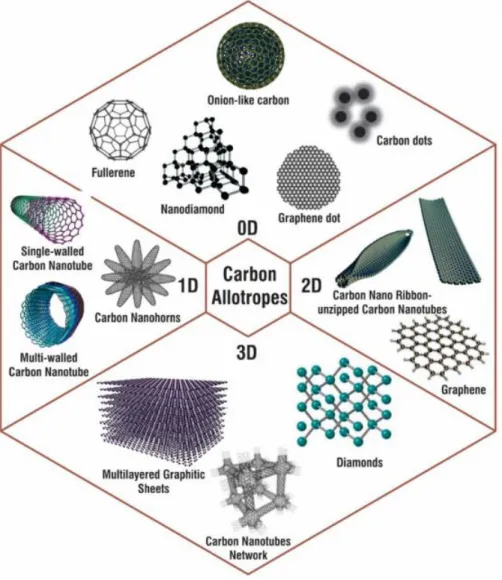
Therefore, as shown in Figure 1.1, carbon allotropes exist for 0D, 1D, 2D, and 3D structures.3 Various carbon allotropes are known, such as CNTs, fullerenes, graphene, diamonds, and graphite.
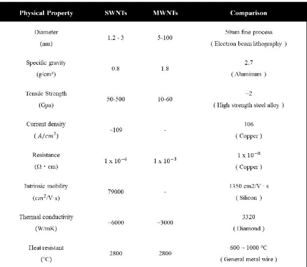
CNTs are light but have strong tensile strength than steel, which have advantages in fine process because of their very small diameter, shown in Table 1. Their thermal and electrical conductivity are similar to that of diamond and copper, also intrinsic mobility is several times superior to that of silicon.
As CNTs have excellent mechanical, electrical, and thermal properties, which distinguish them from other commercial materials, CNTs are being actively studied in various research fields such as transistors45, sensors67, and computers.8
Among various fields, CNTs materials are expected for sensor applications due to their interesting properties and have been studied for electrochemical biosensor components for several decades.9 In addition, chemical functionality of CNTs can be applied to functionalize desired chemical species, which enables to enhance the bio-compatibility and solubility of carbon nanotubes. Particularly, CNTs as nanomaterials have very large surface area to volume ratio, so their reaction with bio-markers on the surface greatly affects the electrical conduction properties of CNTs itself.10 Therefore, when these CNTs are applied to the detection of biomolecules, high-sensitivity signal conversion that wasn’t available in conventional biosensors is possible. Thus, owing to many advantages mentioned above, CNTs biosensors are promising to be the next generation’s building blocks for high-sensitive bio-sensing system.
However, to utilize the excellent properties of CNTs, several problems must be solved in their applications. First, because the size of CNTs is only nanometer scale unlike bulky materials, they are easily bundled each other due to the force of surface energy and van der Waals.11 Because CNTs have large surface areas to volume, they tend to agglomerate to form bundles, lowering the surface energy.
Therefore, to control the carbon nanotubes individually, a technique for dispersing the tubes uniformly is required.
Second, synthesized raw CNTs have mixed electrical properties of metallic and semiconducting depending on the rolling direction of graphene sheets.12 Since metallic CNTs destroy the intrinsic of semiconducting CNTs, the electrical properties of carbon nanotubes must be separated.
2
Figure 1.1. Allotrope structures of carbons depending on dimensions
3
Table 1. Physical and electrical properties of SWNTs and MWNTs
4
1.2 Structures and electrical properties of carbon nanotubes
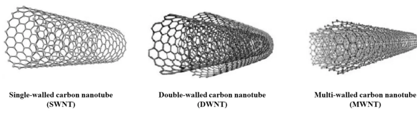
The structures of carbon nanotubes are in form of rolled graphene of which carbons are arranged in a hexagonal shape continually. By the number of rolled graphene sheet, CNTs can be classified by single walled carbon nanotubes (SWNTs) with one rolled sheet, double walled carbon nanotubes (DWNTs) with two rolled sheets, and multi walled carbon nanotubes (MWNTs) with several rolled sheets as shown in Figure 1.2.11
MWNTs have powerful thermal and mechanical properties and low costs due to their mass production.
SWNTs are mainly used for transistors and sensors because their optical and electrical properties are superior to those of MWNTs.
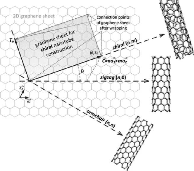
The atomic structures and electrical properties of CNTs can be classified according to chirality again, which indicates the angle of which a graphene sheet is rolled up.13 Chirality can be defined as a chiral angle θ and chiral vectors. In Figure. 1.3, a graphene sheet with defined chiral angles and vectors and different SWNTs structures by chirality can be seen.
The lattice structure of carbons in graphene can be represented by unit vectors and the chiral vectors can be explained by the formula of unit vectors and lattice translational indices (n, m).
𝑪𝒉
⃗⃗⃗⃗ = 𝒏𝒂⃗⃗⃗⃗⃗⃗⃗⃗ + 𝒎𝒂𝟏 ⃗⃗⃗⃗⃗⃗⃗⃗⃗ 𝟐 𝑪𝒉
⃗⃗⃗⃗ ∶ 𝑐ℎ𝑖𝑟𝑎𝑙 𝑣𝑒𝑐𝑡𝑜𝑟, 𝒂⃗⃗⃗⃗ , 𝒂𝟏 ⃗⃗⃗⃗ ∶ 𝑢𝑛𝑖𝑡 𝑣𝑒𝑐𝑡𝑜𝑟𝑠, (𝒏, 𝒎) ∶ 𝑖𝑛𝑑𝑖𝑐𝑒𝑠 𝟐
where (n,m) are integers to represent the number of steps along the zig-zag carbon bonds of the hexagonal lattice.
The chiral angle θ which determines the degrees of twist of tube is defined as the angle (θ) between vectors 𝐶⃗⃗⃗⃗ ℎ and 𝑎⃗⃗⃗⃗ , where θ varies in range of 0°≤|θ|≤30°. 1
𝐬𝐢𝐧 𝛉 = √𝟑𝒎
𝟐√𝒏𝟐+ 𝒎𝟐+ 𝒏𝒎
𝐜𝐨𝐬 𝛉 = 𝟐𝒏 + 𝒎 𝟐√𝒏𝟐+ 𝒎𝟐+ 𝒏𝒎
𝐭𝐚𝐧 𝛉 = √𝟑𝒎 𝟐𝒏 + 𝒎
5
In geometry structures of carbon bonds, there are two achiral SWNTs known as armchairs (θ = 30°) and zigzags (θ = 0°). In addition, It is called ‘chiral’ when the (n,m) indices are n ≠ m and chiral angle is 0°≤|θ|≤30°.
(n − m = 3q, then SWNT is a metallic tubes, n − m ≠ 3q, then SWNTs are semiconducting tubes, where q is an integer)
The diameter of CNTs can be calculated using the equation below, since the interatomic spacing between carbon atoms is known.
𝐝 = 𝟎. 𝟕𝟖𝟑√𝒏𝟐+ 𝒎𝟐+ 𝒏𝒎
6
Figure 1.2. Types of carbon nanotubes depending on different number of walls being rolled up
Figure 1.3. Graphene sheet with defined chiral angles and vectors and various SWNTs structures depending on chirality
7
1.3 Purification method of selective dispersion by conjugated polymers
Selective enrichment of SWNTs is crucial because a variety of electronic device applications require individually dispersed tubes with undamaged structure. Many studies are being carried out to sort mixed m-SWNTs and sc-SWNTs and to disperse SWNTs itself that are aggregated to form bundles simultaneously. Several separation methods of sc-SWNTs were described below.
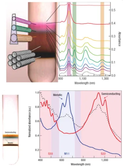
The first method to be introduced is DGU (density gradient ultracentrifugation) which uses density differences of carbon nanotube’s diameters as shown in Figure 1.4. After absorbing the surfactants SDS and sodium cholate on carbon nanotubes for dispersing, a high-speed centrifuge was applied to separate each layers with different electrical properties.14 In general, sorted SWNTs are used for device fabrication without removing the surfactants to prevent SWNT’s bundling.15 In this cases, the surfactants surrounding the SWNTs lower the electrical conductivity of the FETs and reduce the performances.
The second method is agarose gel chromatography, shown in Figure 1.5, which uses hydrogels to separate sc-SWNTs from raw SWNTs. Although the agarose gels are strongly absorbed with sc-SWNTs of various structures, there is a limit to the separation of high-purity sc-SWNTs due to their low selectivity to sc-SWNTs.16
DNA wrapping, the third, is a method of sorting specific chiral carbon nanotubes along the helix direction of DNA synthesized by controlled sequence as shown in Figure 1.6.17 Although it has the advantage which high purity sc-SWNTs can be obtained by isolating only one type of chirality, DNA synthesis is difficult and expensive, and it is not suitable for mass productions.18
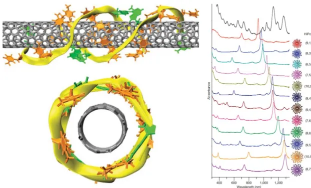
The last method is to use the π-π interaction between SWNTs and conjugated polymer to disperse sc- SWNTs selectively as shown in Figure 7. After Nicholas' group obtained selectively separated sc- SWNTs by poly-fluorene derivations, technologies of separating sc-SWNTs using a conjugated polymer with specific structure are actively in progress.19 This method has the advantage that sc-SWNTs are simultaneously separated and dispersed by the wrapping polymers. Various conjugated polymers such as diketopyrrolopyrroles20, polyfluorenes21 22, polycarbazoles23 24 and polythiophenes25 26 have been studied for selective dispersions of SWNTs.
The selective dispersions by conjugated polymer are affected by variables such as the structure of the conjugated polymer, polymer concentration in solution, type of carbon nanotubes, solvent effects, sonication temperature and time, etc.
8
In conjugated polymer structure, the backbone chain plays an important role in selectivity, and the sorted chirality is determined by the wrapping angle of the backbone chain and the type of derivations of copolymer.1927 The alkyl side chains length of the conjugated polymers determine the types of carbon nanotubes for wrapping.22 It has been reported when the lengths of the side chains are increased, it is possible to sort carbon nanotubes with a larger diameter. The molecular weight of a polymer is another factor that affects selective dispersion.28 There is a report that polymers with a molecular weight of 10 kDa or more can be used successfully as wrapping polymers to obtain efficient charge mobility of electronic devices. Even if a bundle containing a large amount of metallic carbon nanotubes is used, there is a result that high-purity sc-SWNTs can be obtained by polymer wrapping.29
Among them, poly fluorene derivatives were used to selectively disperse SWNTs and provide much improved optical spectra. This demonstrates the potential to selectively sort high purity of sc-SWNTs.19
27
9
Figure 1.4. Density gradient ultracentrifugation (DGU) method
10 Figure 1.5. Agarose gel chromatography method
11 Figure 1.6. DNA wrapping method
Figure 1.7. Conjugated polymer wrapping method with polyfluorene
12
1.4 Single walled carbon nanotubes field effect transistors
For decades, researchers have been leading innovation by downsizing the silicon transistors, the building blocks of many industries. Silicon transistors are now approaching the fundamental limit of which devices can no longer be made smaller. Therefore, researchers are looking for other materials to replace silicon.30
One of the most promising alternatives is to produce field effect transistors (SWNTs-FETs) of single walled carbon nanotubes. SWNTs-FETs are promising because of their high carrier mobility. Also SWNTs can be more energy efficient than conventional metal oxide semiconductor (MOS) FETs for ten times because SWNTs have good electrostatic properties and electron’s transport is ballistic. 31 32 Additionally, transistors fabricated by individual SWNTs with short gate lengths outperform the silicon metal oxide semiconductor transistors in terms of intrinsic performances and power consumptions.33
But, SWNTs FETs with these superior performance over silicon MOS FETs haven’t been realized at technology nodes due to several problems with SWNTs materials itself. The first problem is bundling of SWNTs caused by van der Waals forces and the mixed electrical properties, which are the problems of the SWNTs itself as mentioned. If high-purity of sc-SWNTs solution is obtained by polymer wrapping technology, the bundling problem can be solved and only sc-SWNTs are sorted, making it possible to manufacture FETs and sensors of high performances.5
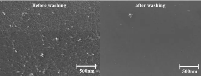
Another problem with SWNTs-FETs is that it is necessary to overcome the disadvantages of the prevailing physical adsorption method and control the appropriate SWNTs density in the film when fabricating FET devices. In FETs fabrication, the SWNTs layer is typically coated by spin coating or dipping the sample in SWNTs inks. However, these methods have the disadvantages of increasing the off current in device performance due to the thick SWNT layer by accumulation and requiring multiple coating cycles or long-term immersion for more than 24 hours.34 3536 Also, this physical adsorption causes the SWNT film to be easily exfoliated off by external forces, resulting in poor film stability as shown in Figure 1.8. Additionally, for technical application of sc-SWNTs solutions in FETs to be realized, it is necessary to place numerous single nanotubes in the designated active region on wafer.5
13
Figure 1.8. SEM image of physical absorption SWNTs film by spin coating before and after washing process.
14
1.5 Electrochemical biosensors based on carbon nanotubes
Studies is continuing to apply carbon nanotubes with excellent mechanical and electrical properties to biosensor fields. By the surface modification technology that functionalizes the surface of carbon- nanotubes, it is possible to study the molecules such as cells, proteins, and DNA.
In general, the electrical sensing operates on the principle which physical or chemical change in a carbon nanotube surface with biomaterial induces some change in electrical properties. Bio-markers (DNA, proteins, etc.) and target materials are polymeric materials which have similar sizes with nanostructures. So even a small variation can have greater effects on nanostructures of SWNTs compared to general small molecules.10
In addition, in case of SWNTs, the ratio of volume to surface areas is very large so the reaction with biomolecules greatly affect the electrical conduction properties of the tubes. Therefore, when these carbon nanotubes are applied to the electrical detection, high-sensitivity signal conversion not found in conventional biosensors is possible.
However, the SWNTs films used in normal SWNTs-biosensor have weak stability, so there is a reliability problem that the electrical intrinsic properties of SWNTs films change depending on washing process of the biosensor.37 For this reason, when comparing resistance changes before and after the immobilization process for biomarker detection, the number of samples used in papers is insufficient to determine the tendency of resistance. This is a problem that must be solved as it reduces the reliability of the sensor.38
15 1.6 Motivations
Single walled carbon nanotubes, the next-generations semiconductor materials, are promising candidates for their excellent electrical properties. However, in synthesis process, SWNTs have mixed electrical properties of semiconducting and metallic, so there are limitations in electrical properties.
Using the conjugated polymer wrapping method, it was attempted to sort sc-SWNTs with high purity without structural damage.
In general, for SWNTs film formation, most methods of manufacturing film by spin-coating the SWNTs ink or immersing the sample in the SWNTs ink. But, this approach has the disadvantages of taking long time and increasing the off-current for device performance due to the accumulated SWNTs layer. According to other paper, it was reported that formation of high density SWNTs is very important and the fabricated films had poor stability to water and organic solvents.39 The poor stability to solvents also caused the problem that the intrinsic electrical properties of the SWNTs film fluctuated depending on washing process when fabricating sensors.
To solve these problems, we report the chemical immobilization of SWNTs on a substrate with a wrapping polymer that can form chemical bonds between sc-SWNTs and an adhesive layer. It was attempted to achieve dense and firmly immobilized SWNTs networks in short time using wrapped SWNTs solution, and the density of SWNTs was controllable according to the reaction time. A patterned SWNTs film can be obtained without a photo resist through a simply pre-patterned adhesive layer, and a SWNTs FETs with a top contact structure was fabricated by this SWNTs films. Since the device is manufactured by accurately dividing the channel region, patterned SWNTs FETs are expected to have superior performances and homogeneities by minimizing interference and leakage current between devices compared to the un-patterned FETs.
After that, linkers and antibodies were immobilized on SWNTs, and antigen was detected by measuring the electrical resistance response changes. Because SWNTs were chemically bonded to the substrate, the SWNTs film will not be exfoliated by washing process required for biosensor manufacturing, so it is likely to maintain the same electrical properties before and after washing. Also, a consistent resistance change trend is expected even when the electrical resistance of each bio-process is measured through many samples.
16 2. Experimental Methods & Materials
2.1. Materials and Characterization
Rn220 SWNTs were purchased from Nano Integris and other starting materials were purchased from TCI and Sigma Aldrich. 525μm thick Si/SiO2 wafers ((100), SiO2 thickness : 100 nm) were purchased from CK plas. Silicon wafer was cleaned with piranha treatment for 7/3 volume ratio of H2SO4/H2O2
mixture for 30min, washed with water and toluene followed by bath sonication in 10min and dried with nitrogen.
1H NMR spectrums were measured by Bruker AVANCE III 300 MHz spectrometer. Using gel permeation chromatography with poly styrene and poly methyl methacrylate as standard materials all synthesized polymer's weight average molecular weight(Mw), number average weight(Mn) and Poly Dipersity Index(PDI = Mw/Mn) were measured at 40 °C.
FT-IR spectrums of polymers and monomers were obtained by Thermo Scientific Nicolet 6700. Uv- Vis Spectrum of films and solution were measured by UV-vis spectrophotometer of Thermo Scientific Evolution 600. Raman spectrum of SWNT film were measured by Thermo Scientific DXR spectrometer.
2.2. Materials Synthesis
Scheme 1. Synthesis of benzophenone silane-based SAM (BPS).
2.2.1. Synthesis of 4-(Allyloxy)benzophenone, ABP
ABP monomers was synthesized via a previously reported paper.40 (yields : 82%).1H NMR (300 MHz, CDCl3) δ 7.85-7.80 (m, 2H), 7.77 – 7.71 (m, 2H), 7.61 – 7.52 (m, 1H), 7.51 – 7.43z (m, 2H), 6.99 (d, J
= 8.9 Hz, 2H), 6.13 – 6.01 (m, 1H), 5.48 – 5.31 (m, 2H), 4.64 – 4.60 (m, 2H).
2.2.2. Synthesis of 4-(3’-Chlorodimethylsilyl) –(propyloxy)benzophenone, BPS
BPS monomers was synthesized via a previously reported paper.401H NMR (300 MHz, CDCl3) δ 7.92 (m, 2H), 7.83 (m, 2H), 7.60 (m, 1H), 7.53 – 7.47 (m, 2H), 7.02 (m, 2H), 4.09 – 4.01 (m, 2H), 1.99 – 1.91 (m, 2H), 1.06 – 0.95 (m, 2H), 0.25 – 0.22 (s, 6H).
17 Figure 2.1. 1H NMR spectrum of ABP
18
Scheme 2. Synthesis of alkyne-functionalized monomers (DPAP), and clickable random acrylate copolymers, P(DPAP-r-PA)
2.2.3. Synthesis of 5-acryloyloxyisophthalic acid, APA
The synthesis routes of APA are shown in Scheme 2. In three-necked round bottom flask, 5- hydroxyisophthalic acids (5-HPA, 2 g, 11 mmol) were added to 20 mL of 2M NaOH solution and this reaction mixtures were stirred in an ice bath about 20min at 4 °C. At this temperature, acryloyl chlorides (1.04 g, 11.6 mmol) were added dropwise to the mixture solution for 1h and then stirred at RT for 1h.
Upon adding diluted cool HCl solutions to mixtures to neutralize at pH 7, the APA products started to precipitate as white powders. Then APA was filtered and washed by DI water. The white products were recrystallized from methanol (yield : 57%) and put in a vacuum oven at 40 °C for one night. 1H NMR (300 MHz, DMSO-d6) δ 13.51 (s, 2H), 8.36 (t, 1H), 7.95 (d, 2H), 6.55 (d, 1H), 6.44 (d, 1H), 6.21 (d, 1H).
19 Figure 2.2. 1H NMR spectrum of APA
2.2.4. Synthesis of Di(propargyl)-5-(Acryloxyloxy)isophthalate, DPAP
The synthesis routes of DPAP are shown in Scheme 2. In two-necked round bottom flask, APA (1.27 g, 0.3 mmol) and 4-dimethylaminopyridine (DMAP, 0.023 g, 0.19 mmol) were added. Degassed propagyl alcohol (PA, 0.96mL, 12.7 mmol) in 4mL of THF was injected drop by drop to reaction crude.
The mixture were cool down in an ice bath to 4 °C for 30min under nitrogen atmosphere. 3-dicyclohexyl carbodiimid (DCC, 0.392 g, 1.9 mmol) dissolved in 3mL andyrous THF was added dropwise and stirred in an ice bath for 4 h. The crudes were allowed to attain at RT and kept for 20 h under stirring. The solvent was removed by an evaporator and crudes were dissolved in chloroform and filtered. Using 10%
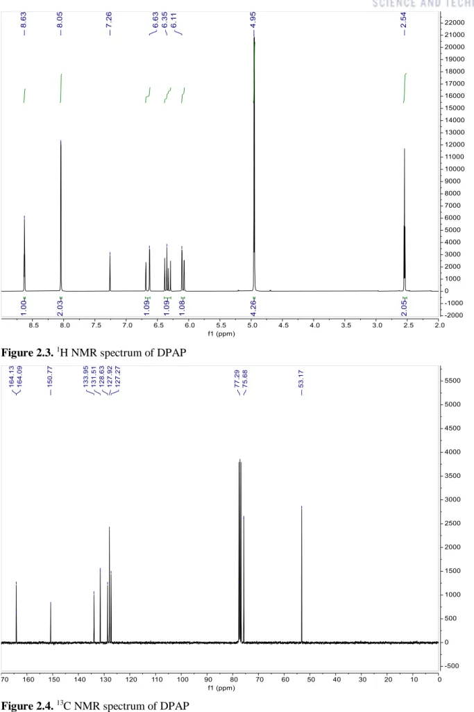
bicarbonate solution, organic layer was washed twice. Then using hexane and ethyl acetate, the residue were purified by silica column giving the product as white powders (yield : 28%). 1H NMR (300 MHz, CDCl3) δ 8.63 (t, J = 1.5 Hz, 1H), 8.03 (d, 2H), 6.68 (m, 1H), 6.36 (m, 1H), 6.11 (m, 1H), 4.94 (d, 4H), 2.53 (t, 2H). 13C NMR (75 MHz, CDCl3) δ 164.11, 164.07, 150.75, 133.93, 131.50, 128.62, 127.91, 127.28, 77.27, 75.69, 53.16.
20 Figure 2.3. 1H NMR spectrum of DPAP
Figure 2.4. 13C NMR spectrum of DPAP
21 Figure 2.5. GC-MS of DPAP
22
2.2.5. Synthesis of poly(dipropargyl-5-(acryloyloxy)isophthalate-r-propargylacrylate, P(DPAP- r-PA)
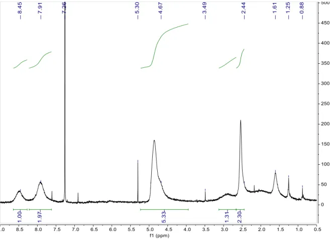
The synthesis routes of P(DPAP-r-PA) are shown in Scheme 2. In schlenk flask, DPAP (0.5 g, 1.6 mmol), AIBN (5.2mg, 0.0052 mmol) and propargyl acrylate (0.16 mL, 1.6 mmol) were added to 1.2 mL dry DMF. Under nitrogen, the reaction mixtures were stirred for 24 h at 75 ℃. The crudes were dissolved in chloroform and precipitated in diethyl ether twice. The collected product was dried in vacuum oven at 40 °C, giving the polymer as yellow powder (0.324 g, 24%). Mn = 20.3 kDa, PDI= 2.3.
1H NMR (300 MHz, CDCl3) δ 8.47 (br, 1H), 7.92 (br, 2H), 4.86 (br, 5H), 2.93 (br, 1H), 2.52 (br, 2H)
Figure 2.6. 1H NMR spectrum of P(DPAP-r-PA)
23
Scheme 3. Synthesis of clickable azide group-functionalized polyfluorene, P(FD-N3) 2.2.6. Synthesis of 2,7-dibromo-9,9-bis(12-bromododecyl)9H-fluorene, FD-Br
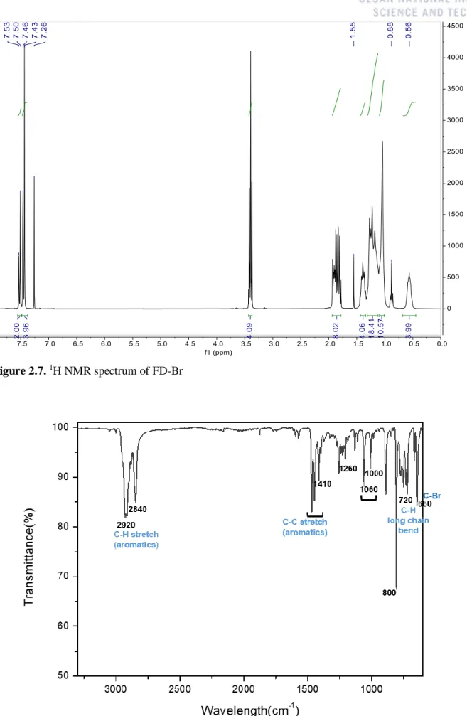
In schlenk flask, 2,7-dibromo-9H-fluorene (7.5 g, 23 mmol) and 1,12-dibromododecane (2.5 g, 7.72 mmol) were added to 30 mL of toluene. Under nitrogen, the reaction mixtures were stirred for 20h at 80 ℃. After that, the crudes were extracted by Chloroform and the organic phases were rinsed with water. Using hexane, the residues were purified by silica column and recrystallized by ethanol and hexane to obtain the product as white solids (4.00g, 64%). 1H NMR (300 MHz, CDCl3) δ 7.49- 7.44 (m, 6H), 3.38 (m, 4H), 1.86 (m, 8H), 1.38 (br, 4H), 1.33-1.11 (m, 18H), 1.01 (s, 10H) 0.62 (br, 4H).
24 Figure 2.7. 1H NMR spectrum of FD-Br
Figure 2.8. FT-IR spectrum of FD-Br
25
2.2.7. Synthesis of 2,7-dibromo-9,9-bis(12-azidododecyl)9H-fluorene, FD-N3
In two-necked round bottom flask, FD-Br (7.2g, 8.78 mmol) and sodium azide(2.28 g, 35 mmol) were added in 12mL of DMF. Under nitrogen, the reaction mixture were stirred at 80 ℃ for 12 h. After that, the crudes were extracted by chloroform and the organic phases were rinsed with water. Using hexane and ethyl acetate, the residues were purified by silica column and recrystallized by ethanol and hexane to obtain the product as white solids (5.36 g, 83%). 1H NMR (300 MHz, CDCl3) δ 7.49- 7.44 (m, 6H), 3.25 (m, 4H), 1.91 (m, 4H), 1.57 (m, 4H) , 1.40-1.01 (br, 32H), 1.08 (br, 10H) 0.57 (br, 4H).
Figure 2.9. 1H NMR spectrum of FD-N3
26 Figure 2.10. FT-IR spectrum of FD-N3
27
2.2.8. Synthesis of 2,2'-(9,9-didodecyl-9H-fluorene-2,7-diyl)bis(4,4,5,5-tetramethyl-1,3,2- dioxaborolane), FD-pinacolborane
In schlenk flask, 2,7-dibromo-9,9-didodecyl-9H-fluorene (5 g, 7.56 mmol), bis(pinacolato)diboron (4.607 g, 18.144 mmol), potassium acetate (3.71 g, 37.8 mmol) and 1,1′-Bis(diphenylphosphino) ferrocene]dichloropalladium(II) (0.1668 g, 0.2268 mmol) was added in 50 mL of anhydrous dioxane.
Under nitrogen, the reaction mixtures were stirred at 105 ℃ for 72 h. After that, the residues were extracted by chloroform and the organic phases were rinsed with water. Using activated carbon, the residues were purified by silica column with dichloromethane and recrystallized by methanol and acetone to obtain the product as white solids (3.98 g, 70%). 1H NMR (300 MHz, CDCl3) δ 7.85- 7.65 (m, 6H), 1.99 (m, 4H), 1.39 (m, 24H), 1.30-0.95 (m, 36H), 0.86 (m, 6H), 0.53 (br, 4H).
Figure 2.11. 1H NMR spectrum of FD-pinacolborane
28 Figure 2.12. FT-IR spectrum of FD-pinacolborane
29
2.2.9. Synthesis of poly(didodecylfluorene-alt-bis-azidododecyl-fluorene), P(FD-N3)
In schlenk flask, FD-N3 (0.2264 g, 0.3 mmol), FD_pinacolborane (0.2228 g, 0.3mmol), tris(dibenzylideneacetone)dipalladium(0) (0.0054 g, 0.006 mmol) and tris(o-tolyl)phosphine (0.0073 g, 0.024 mmol) were added in 6 mL of degassed toluene. Under nitrogen atmosphere, 0.78 mL of degassed 25 wt% aqueous tetraethyl ammonium hydroxide solution was added drop by drop to the reaction mixtures. Then the crude were stirred vigorously for 6 h at 85 ℃. After that, the crude was extracted by chloroform and the organic phases were rinsed with water three times. Then the polymer was precipitated in MeOH and soxhleted with methanol and chloroform. The collected product was dried in vacuum oven at 50 °C giving the polymer as yellow powder (0.2118 g, 63%) . Mn = 2.3 kDa, PDI= 2.1,
1H NMR (300 MHz, Chloroform-d) δ 7.84 (m, 4H), 7.70 (m, 8H), 3.24 (m, 4H), 2.16 (m, 4H), 1.58 (m, 4H), 1.19 (m, 80H), 0.88 (m, 6H).
Figure 2.13. 1H NMR spectrum of P(FD-N3)
30 Figure 2.14. FT-IR spectrum of P(FD-N3)
31
Scheme 4. Schematic process of selective enrichment of sc-SWNTs by conjugated polymer wrapping method
2.3. Enrichment of the selectively sc-SWNTs dispersion by polymer extraction
The enrichment processes were conducted by dispersing 15 mg of Rn-220 SWNTs in 40 mL of toluene with 20mg of P(FD-N3). After cooling, the mixtures were homogenized using horn sonicator (Sonics & Materials Inc, VCX-750, micro-tip, ϕ5 mm) about 1h 30min at 5 ℃. Then the dispersed solutions were centrifuged at 85,000 g for 30min to separate the sc-SWNTs (Hanil Scientific Inc., Supra R30). After centrifuge process, the supernatant solution of wrapped sc-SWNTs was carefully extracted.
For higher purification of sc-SWNTs, 30 mg of silica gels were added into the supernatant solution. The mixtures were sonicated in ice bath sonicator (Hwashintech, power sonic 520) for 30min at 5 ℃ followed centrifuged at 85,000 g for 30min again. The supernatant solution were collected and filtered with 0.20 μm MCE membrane. Collected P(FD-N3) wrapped sc-SWNTs on filter paper were rinsed with toluene several times to remove unbound P(FD-N3) polymer. The solid was re-dispersed in toluene about 10 min.
32 2.4. BPS immobilization on SiO2 surface
The silane groups of BPS was immobilized on SiO2 surface by immersing Si/SiO2 wafers to 0.1M toluene solutions with BPS. The solution with wafers were lefted overnight, the samples were washed with ethanol and toluene in bath sonication each 3min before being dried under nitrogen stream. Film formation of BPS was determined by contact angle measurement.
2.5. Formation of alkyne-functionalized patterned polymer film by UV attachment
5 mg/mL solution of P(DPAP-r-PA) in dioxane was spin-coated onto monolayer of BPS on silicon wafer. Using shadow masks, polymer coated film was exposed to UVA lamp (727 mJ/cm2) directly about 90s for photochemical attachment of polymer films. Only polymer exposed to UV light was anchored by UV cross-linking with BPS. Then the film was washed by chloroform for 1h in bath sonication to remove the unreacted polymer and dried by nitrogen stream to remove chloroform.
2.6. Procedure of Click reaction in SWNTs solution
In 50 mL vial, 1 mL solution of separated sc-SWNTs (0.02 mg/ml) and an alkyne polymer functionalized wafer (size : 15 × 20 mm) was added and purged by nitrogen stream for 5min. Copper(Ⅱ) sulfate pentahydrate (3 mg, 0.012 mmol) and sodium ascorbate (19mg, 0.096 mmol) were added to 0.5 mL of DI water and purged by nitrogen stream for 5min. Then the mixture of catalyst solution was add to sc-SWNTs solution with wafer. The reaction mixtures were sonicated in bath sonication (90-120 W) at 55 °C. Then Click reacted wafer was rinsed with DI water, methanol, acetone and toluene by sonication for each 30 min to remove unreacted catalysts and sc-SWNTs.
2.7. Electrode deposition for top contact structures
Field effect transistors which had immobilized SWNTs as semiconductor layers by Click reaction were fabricated by top-contact structure (SiO2 100 nm). Using Au (60 nm), source/drain electrodes were designed through shadow masks using thermal evaporator at 5.0 × 10⁻⁶ torr with 0.3 Å/s with a parallel type which channel and width lengths are 100 μm and 1000 μm each.
33
Figure 2.15. Shadow masks for electrode deposition (unit of length : mm)
34
2.8. Attachment of antibodies via 1-pyrenebutanoic acid succinimidyl ester (1-PBASE)
Covalent attachment of antibodies to immobilized SWNTs film on the biosensor template was performed by two step procedures. For antibody immobilization, 1-pyrenebutanoic acid succinimidyl esters (PBASE) were used as linkers which connect SWNTs with receptor by noncovalent sidewall functionalization of SWNTs.
In solution of 10mM 1-PBASE in DMF, fabricated devices was immersed overnight at RT. After the incubation, the devices were rinsed by pure DMF and methanol to wash excess 1-PBASE reagents and dried by nitrogen stream. Then electric resistance responses were measured by probe station to confirm 1-PBASE-assembly process.
Aβ antibodies were diluted in solution of phosphate buffered saline (pH 7.4). 100μg/ml Aβ antibodies were self-assembled onto 1-PBASE linker modified SWNTs template overnight at 4℃. After the template was rinsed with PBS solution, bovine serum albumin (BSA, 3wt% in PBS) were treated for 1 h to prevent nonspecific binding. Resistances were measured by a probe station to confirm antibody assembles.
2.9. Detection of Aβ1-42 using the developed SWNTs biosensor
Aβ1-42 was diluted in DMSO solution to make 4mM Aβ1-42 stock. This stock solution then diluted in PBS to make 100pM Aβ1-42 solution. Aβ1-42 solution is dropped on the antibodies immobilized sample and reacted at 4°C for 2 hours. To remove unreacted Aβ1-42, the sample was washed with PBS buffer solution. Detection of Aβ1-42 was confirmed by electrical resistance responses with a probe station according to interactions between anti-Aβ antibodies and Aβ1-42.
35 3. Results and Discussion
3.1. Enrichment of sc-SWNTs dispersion by polymer extraction
Mixed properties and strong intermolecular π-π interactions are unique problems of SWNTs.41 Also unstable immobilization of SWNTs on the substrate and low reproducibility of device are major obstacles in development of SWNTs based biosensors.3537
First, only sc-SWNTs were selectively dispersed by wrapping polymer to solve the mixed properties and bundling caused by π-π interaction of SWNTs. Click reaction was used to solve the remaining problems of low stability and reproducibility of SWNTs film.
For this, polyfluorene polymers known to have high selectivity of semiconducting tubes with large diameters were synthesized.39 This polymer was designed to have long alkyl chain lengths of C12 and azide groups at the end of side chains, which enables to separate large diameter SWNTs with a narrow band gap and form chemical bonds with alkyne groups by Click reaction.
To prepare this polyfluorene derivatives, a monomer called FD-N3 having C12 chain length and azide groups at the end of chains was synthesized from 2,7-dibromofluorene.From 2,7-dibromofluorene, FD- Br was synthesized by alkylation of 1,12-dibromododecane under the reaction TBAB-NaOH catalytic system.42 43 The bromine of FD-Br was substituted with azide group using sodium azide in DMF solution to obtain FD-N3. From 2,7-dibromo-9,9-didodecyl-9H-fluorenes, FD-pinacolborane was synthesized by condensation reaction with bis(pinacolato)diboron.44 The alternating polymer P(FD-N3) was synthesized using FD-N3 and FD-pinacolborane monomers through Suzuki coupling. This synthesized fluorene polymer with azide group was used to purify sc-SWNTs of the plasma torch SWNTs (Nanointegris, RN-220).
Rn220 having large diameters was used because it is known to have high performances than small diameter SWNTs. Polyfluorene, the wrapping polymers, are known to effectively separate sc-SWNTs.
However, if the wrapping polymer contains azide groups of its side chain, it is difficult to separate high- purity sc-SWNTs because metallic SWNTs are also have interactions with polymers containing high concentrations of nitrogen atoms, due to the rich electrons condition of the nitrogen.5 Among the results of the selective dispersions of sc-SWNTs using the conjugated polymer wrapping method, there are some results that the purity of sc-SWNTs was increased as metallic SWNTs are selectively removed by silica gels.45Using the affinity of silica gel and m-SWNTs, high-purity of sc-SWNTs were selectively separated.
36
For selective sorting of sc-SWNTs, plasma torch SWNTs were dispersed in toluene solution of P(FD- N3) polymer with silica gel by horn sonication. After that, supernatant solution of sc-SWNTs wrapped with polyfluorene was obtained by ultracentrifuge. Remaining unwrapped polymer in the extracted suspension was removed by filtration, and enriched SWNTs on filter paper were re-dispersed in toluene.
For unsorted SWNTs, as a reference sample, raw SWNTs bundle was dispersed in sodium dodecylsulfate (SDS) solution dissolved in deionized (DI) water.
The results of selective sc-SWNTs dispersion by conjugated polymers were confirmed by UV-vis and Raman spectrum. The absorption spectrum of the enriched SWNTs was measured to identify the selectively separated species of sc-SWNTs from the solution by UV-vis spectroscopy. As shown in Figure 3.1, peaks of enriched SWNTs showed sharpen semiconducting transition peaks in 700-1100 nm, 450-550 nm bands for S11, S22 respectively after sorting processes. In sample separated by only toluene, slight peak is observed in the M11 (600-750 nm) region, but no peak is observed in the sample separated by silica and toluene.
Figure 3.1. UV-vis-NIR absorption spectra of raw SWNTs and sorted sc-SWNTs
37
For a more detailed analysis of the selective sc-SWNTs dispersion, Raman spectrum was obtained as shown in Figure 3.2. In radial breathing mode (RBM), lattice vibrations of SWNTs is an inherent properties among specific SWNTs. RBM relative intensity can be used to describe the electrical properties of carbon nanotubes.46In the RBM region, sorted sc-SWNTs with 0.9–1.5 nm diameters were investigated with Raman shifts on 100-300 cm–1. With an excitation energy of 1.59 eV (780 nm), the resonant Raman scattering was measured. Since metallic SWNTs with a diameter of 1.3-1.5 nm resonated with an excitation energy of 1.59 eV in this RBM region, the resonance with metallic SWNTs appears near 160 cm-1, as shown in Figure 2.16.47 After the enrichment process using toluene with silica, these metallic peaks wasn’t observed from the Raman spectrum in the same range.
Figure 3.2. Raman scattering spectras of raw SWNTs and sorted sc-SWNTs (laser source 780nm)
38
The damage of SWNTs structure also can be confirmed in RBM mode as shown in Figure 3.3. The Raman scattering spectrum of SWNTs is shown by two strong peaks at 1580 and 2700 cm−1, named G band and G’ band which is represented to intrinsic electrical properties of SWNTs.48 In presence of defects in SWNTs, D band (D means defect or disorder) is observed at about 1350 cm-1. In separated sc-SWNTs sample, the intrinsic peaks of G and G' bands were observed, but the D bands indicating defects were not observed. This result means that m-SWNTs were removed and only undamaged sc- SWNTs were selectively enriched by conjugated polymer wrapping method.
1200 1400 1600 1800
In te n si ty
Raman shift
(
cm-1)
Figure 3.3. Raman scattering spectra of sorted sc-SWNTs (laser source 532nm)
39
3.2. Fabrication of patterned SWNTs field effect transistor
Scheme 5. Schematic process of fabricating patterned SWNTs field effect transistors.
With Click reaction, SWNT films with high stability and robustness was fabricated by chemical immobilization as shown in scheme 5. BPS monolayer is formed on the SiO2 surface of wafer and alkyne functionalized polymer layer was spin-coated, which chemically immobilized the SNWTs layer by Click reaction.
Before polymer coating, the contact angle was measured to confirm the self-assembly of SAM as shown in Figure.3.4. Before the SAM layer assembly, the SiO2 surface of the wafer was hydrophilic by piranha treatment. After the SAM layer is formed, however, the SiO2 surface was hydrophobic due to the effect of the benzophenone functional group.
Figure 3.4. Contact angle after SAM treatment and image of water droplets before and after SAM
40
Covered by shadow mask, the alkyne functionalized polymer layer was exposed to UV lights and unreacted polymer was removed by solvent washing of chloroform. Only irradiated polymer region by UV lights is selectively immobilized to BPS layer and then patterned polymer layer was formed, as shown in Figure 3.5. Because the electrodes were deposited in top contact structure, the channel length was designed for 100 μm, which was relatively wide active region, to make it facilitate to align the electrode. But it was confirmed that the pattern of the adhesion layer is possible up to 20 μm and 5 μm.
A finely patterned polymer layer can be obtained without photolithography, through this simple process as shown in Figure 3.6.
Figure 3.5. Image of patterned adhension layer by UV light attachment
Figure 3.6. Optical microscope images of patterned adhension layers
41
The absorption spectra of a strongly attached polymer film was obtained with little difference in absorption peak height before and after chloroform washing by sonication as shown in Figure 3.7. This is because the polymer layer is chemically attached to the SAM-based substrate and cannot be washed away by solvents. The film thickness of the immobilized P(DPAP-r-PA) polymer film was average 23 nm, which is measured by ellipsometer.
300 400 500
0.0 0.1 0.2 0.3
Absorbance
Wavelength (nm)
P(DPAP-co-PA) before washing P(DPAP-co-PA)after washing
Figure 3.7. Absorbance spectra of P(DPAP-co-PA) films before and after solvent washing
The next step to obtain robust SWNTs films is to chemically react the azide functionalized SWNTs with P(DPAP-r-PA) polymer layer on substrate using Click reaction. The process of immobilizing SWNTs to substrate was carried out as shown in the schematic diagram 6. First, P(DPAP-r-PA) polymer attached substrates were immersed in P(FD-N3)-SWNTs inks and degassed with nitrogen for 5min.
Degassed in nitrogen in same method, copper catalyst and reducing agent are dissolved in D.I water and then injected into immediately SWNT inks. Then Click reaction proceeded between the alkyne of substrate and the azide of the SWNTs by blending the catalyst aqueous solution and sc-SWNTs inks using bath sonication for 5 minutes at 50℃. After the reaction, the remaining catalyst was rinsed in MeOH and DI water by ultrasonication for each 10min and unreacted sc-SWNT was washed with Toluene for 30min, leaving only immobilized SWNTs by Click reaction.
42
Patterned SWNTs film was formed by the Click reaction with the pre-patterned polymer layer and it was confirmed by Raman spectroscopy shown in Figure 3.8. In ① region where the polymer was patterned, the G-band related to sp2 carbon bonding of SWNTs was observed at 1650 cm-1, whereas the D-band related to defects and impurities of carbon didn’t appear at 1350 cm-1. In ② region where the polymer wasn’t patterned, however, G band and D band absorption peaks of SWNT weren’t observed at all. This Raman spectra mean that undamaged SWNTs were immobilized only on the pre-patterned polymer layer to form a new patterned SWNTs film. This results not only mean that SWNTs film had good solvent stability with the substrate in harsh conditions because of the chemical bonds, but also suggested a method of increasing FETs performance and uniformity by setting accurate channel regions.
Scheme 6. Schematic of azide-alkyne cycloaddition reaction
Figure 3.8. Raman scattering spectras of SWNTs on patterned polymer(pink) and on SiO2(black)
43
The density change and stability of the patterned SWNTs film depending on the Click reaction time was observed with the scanning electron microscopy (SEM). In Figure 3.9, the SWNT film density on P(DPAP-r-PA) increased with the reaction time even after harsh washing with solvents.
The stability of SWNTs film to substrate has potential in application of SWNTs FETs that could work in aqueous solution as a biosensor. Particularly, as sensors needs to detect a low-concentration target material, sensing with an accurate active area is very important in terms of device reliability.
In SEM image analysis, the linear density of SWNTs is estimated to be approximately 10, 20, 25, 28, 29, 51 tubes/μm in each sample for a click response time of 30 sec, 1 min, 2 min, 3 min, 5 min and 10 min respectively. Based on the results, the SWNT film density change depending on reaction time was plotted as a graph in Figure 3.10.
The sample that achieved the highest linear density had reaction time of 10 minutes. But as SWNTs are stacked with each other, there was a problem that the SWNTs film thickness was increased rather than a thin and dense SWNTs monolayer. With only 5 minutes of simple Click reaction, linear density of 29 tubes/μm was obtained, which was a sufficient density for transport of charge carriers in percolation paths in random SWNTs networks. To obtain similar density SWNTs film through common physiorption method, several times of spin coating or immersion in SNWT ink for a long time are required.
44
Figure 3.9. SWNTs film samples of different densities with icreased Click reaction time
Figure 3.10. SWNT density change by Click reaction time
100 200 300 400 500 600 0
10 20 30 40 50
C N T d en si ty ( n u mber /μm )
Reaction Time (s)
45
To confirm the electrical properties of the fabricated SWNTs films, source and drain electrodes were deposited on the SWNTs networks for structure of top contact bottom gate FETs. In addition, for carrier mobility calculation, the capacitance value of dielectric layer composing with P(DPAP-r-PA) and silicon oxides. 100nm SiO2 has a rather high capacitance per unit of area of 34.5nF/cm2, whereas that of P(DPAP-r-PA) is 26.0nF/cm2. Also the carbon nanotubes FETs exhibit bipolar behavior itself, however, they exhibit p-type characteristics by adsorption of moisture in the atmosphere.
To identify the advantages of active region’s patterning, it was compared with samples which have coated active layers on the entire wafer without patterning. First, in case of the un-patterned sample of which devices weren't individually isolated, the SWNTs of the entire wafers worked as an active region.
Therefore, it was impossible to properly measure the output curve (a) and transfer curve (b) due to the high leakage current and interference between devices as shown in Figure 3.11.
Figure 3.11. Fabricated un-patterned SWNTs FET by Click reaction without isolation
Another comparison of physically isolated SWNTs FETs (a) and chemically patterned SWNTs FETs (b) was represented by schematic diagrams of output curves and transfer curves in Figure 3.12. As shown in the I-V curves, the most obvious advantage of the sample with patterned active regions is that the deviation of the transfer curve is significantly reduced compared to the sample of which devices were isolated physically by cutter. Also, the output curve shows a much improved current value. The table summarizes the electrical carrier mobility (μ) and on/off ratio for each structured transistor.
First, un-patterned samples with isolation process had an average on-state current of 4.23 × 10⁻⁶ A and an average on/off ratio of 1.83 × 10⁶ A with a maximum carrier mobility of 3.5313 cm2/V·s. On the other hand, samples with patterned SWNTs layer had a average on-state current of 4.75 × 10⁻⁵ A and an average on/off ratio of 1.56 × 10⁷ A with a maximum carrier mobility of 18.0814 cm2/V·s.
46
Improved device performances such as carrier mobilities, on/off ratio, and on currents are the result of accurately separated channel regions between the source and drain electrodes. In case of isolated sc- SWNTs film, since it has relatively wide active regions, there are many paths for charge carriers, so the device has poor reliability. But, sc-SWNTs film that are precisely patterned only between source and drain showed improved performance by minimizing leakage currents and interferences between devices.
Figure 3.12. Electrical performance comparsion of patterned FET and unpatterned FET with isolation
47 3.3. Applications to biosensors
Scheme 6. Schematic process of fabricating patterned Alzheimer’s biosensor
SWNTs materials have great potentials for biosensor applications due to their small sizes, chemical functionality and excellent electrical properties. In this study, the fabricated SWNTs FETs was studied for application to biosensors. Among various biomarkers, a biosensor technology of detecting Aβ1-42 which can be used for Alzheimer's diagnosing disease, was developed.
For confirming film stability to washing process, SWNTs were immobilized on sensor platform and resistance responses were measured. After that, to determine the effects of PBS buffer on the device performances, the resistance value was measured after bath sonication in PBS solution for 10 minutes.
As shown in Figure 3.13, I-V curves were measured before and after washing with PBS buffer with 20 samples. In the I-V curve, the plot before and after washing was almost the same, and the average resistance value was 0.53 MΩ before washing and 0.59 MΩ after washing, showing no significant difference. This means that SWNTs film wasn’t exfoliated by the PBS buffer due to the chemically bonded SWNTs to the substrate, which means that the reliability problem caused by unstable SWNTs layers in existing bio-platform has been solved.
48
Figure 3.13. Comparison of I-V curve and resistance change before and after washing with PBS solution to confirm the stability of SWNT films on the sensor. Error bar represents standard devication (n=20)
To immobilize the antibody to the anchored SWNTs sensor platforms, linkers were required between the SWNTs surface and the antibody.49 The hydrophobic pyrenyl groups of 1-PBASE used as linkers were adsorbed to the hydrophobic sidewall of SWNTs through 𝜋-𝜋 stacking interactions irreversibly.
Aβ antibodies used for target antigen detection were immobilized by nucleophilic substitutions of primary and secondary amine groups with succinimide groups in 1-PBASE as a linker.50
The sequence of processes was confirmed by measuring the resistance responses (0.53 MΩ, 0.70 MΩ, 7.65 MΩ) of SWNTs, 1-PBASE adsorbed on SWNTs, and antibodies immobilized to adsorbed 1- PBASE, respectively. As shown in Figure 3.14, the 𝜋-𝜋 interactions of 1-PBSE with SWNTs surface didn’t significantly change the resistance values of SWNTs sensor platforms. Immobilization of antibodies via 1-PBASE significantly increased the resistance values of the biosensor. Compared to 1- PBSE adsorption process, the reason for the significant increase in resistance after Aβ antibodies immobilization is that negative charges are transferred from antibodies to SWNTs with p-type semiconductor properties.51