17 Figure 2.8 Low- and High-magnification TEM images and the selected area diffraction patterns for ZnO (a, c, e) and CuO (b, d, f) nanowire respectively. 29 Figure 3.2 SEM images of tilted view for selective growth and surface of patterned substrates covered with nanowires. 36 Figure 3.6 H2 responses of three junctions (p-p, n-n and p-n) in two different samples to see the reproducibility of the measurements.
40 Figure 3.9 (a) Schematic illustration of 3x3 sensor array and (b) results of an LDA analysis of the obtained sensitivities for the sensor array.
INTRODUCTION
One-dimensional (1-D) metal-oxide nanostructures
- Characteristics of 1-D metal-oxide nanostructures
- Chemical sensing behavior of 1-D metal-oxide nanostructures
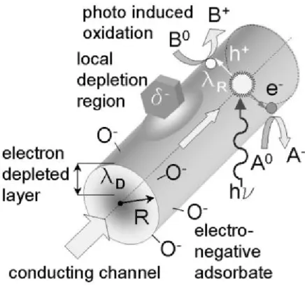
This does not apply to those of quasi-one-dimensional oxide nanostructures (i.e. systems with diameters less than ~100 nm), which are expected to possess novel characteristics for the following reasons.15 First, a large surface area-to-volume ratio that a significant A fraction of the atoms (or molecules) in such systems are surface atoms that can participate in surface reactions. As a result, one can imagine situations where the conductivity of a nanowire could vary from a completely non-conductive state to a highly conductive state, based entirely on the chemistry taking place on the surface. The increased diffusion rate of electrons and holes to the surface of the nanodevice ensures that the analyte is rapidly photodesorbed from the surface (~few seconds), even at room temperature.
Finally, as the diameter of the nanowires is reduced, or as their material properties are modulated along the radial or axial direction, one can expect a series of increasingly significant quantum effects16.
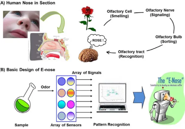
Electronic Nose (E-nose)
- Concept of E-nose
- Characteristics of E-nose: Sensitivity and Selectivity
To improve orthogonality in reactions in practical e-nose systems, it is particularly desirable to integrate one-dimensional nanostructure with different morphologies and compositions with small dimensions and high surface-to-volume ratios on a single substrate. However, to minimize the manufacturing costs and increase the yield of these types of devices, it would be a promising direction if multiple types of nanowires could be grown directly and simultaneously on desired locations of the substrates without any interaction between them33. To improve orthogonality in reactions and increase yield in practical multielectrode e-nose systems, it is desirable to integrate 1-D nanostructure with different morphologies and compositions with small dimensions and high surface area-to-volume ratios on a single substrate .
To increase the sensitivity, palladium (Pd) nanoparticles were decorated on the junction and compared with pristine and Ag-decorated junctions for the capability of e-nose sensors.
ALTERNATIVELY DRIVEN DUAL NANOWIRE ARRAYS BY ZnO AND CuO FOR
EXPERIMENT
- Alternatively driven dual nanowire arrays
- Analysis
- Gas sensor fabrication using single ZnO and CuO nanowire
- Gas response test toward H 2 , CO and NO 2
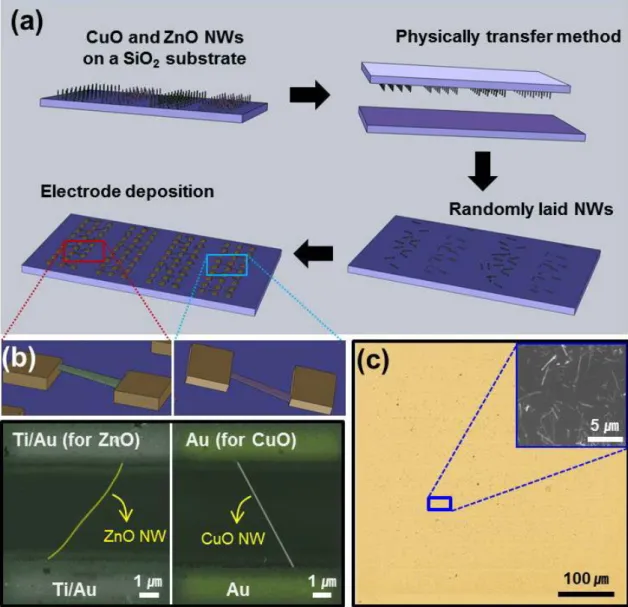
First, 800 nm-thick Zn and Cu metal films were deposited on a single substrate by the e-beam evaporation, which were patterned and separated by the distance of 5 µm via a conventional lithography. The identity and morphology of the resulting one-dimensional (1-D) nanostructures were determined by scanning electron microscopy (SEM), X-ray diffraction (XRD), transmission electron microscopy (TEM) and energy dispersive X-ray spectroscopy (EDS). To investigate the influence of three gases (H2, CO and NO2) on the carrier transport inside the nanowires, a simple sensor was fabricated by transferring the multiple nanowires (ZnO, CuO) by direct contact onto a clean p-type silicon wafer covered with a 200 nm thick silica film, which served as an insulating layer.
The transfer was performed by gently pressing the nanowire-covered substrate onto the Si wafer (shown in Figure 2.3). The source and drain electrodes were fabricated using conventional photolithography where the Au (200 nm, for CuO nanowires) or Ti/Au (10/200 nm, for ZnO nanowires) electrodes were deposited using an e-beam evaporator, respectively, by a shadow mask properly. placed over linear sets of both nanowires. A representative series of source-drain currents, ISD, measured as a function of time at an applied source-drain voltage of 1 V is shown in Figure 2.12 for some ZnO and CuO nanowires.
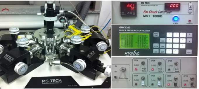
Gas sensors were measured in a probe chamber equipped with an electrical measurement system (KEITHLEY 2636A), a temperature control system, and a precision gas flow system. One of the three gases (~100 ppm), balanced with dry air, was introduced into the chamber under 1 atm of dry background air. Sensitivity is defined as S=(Ig-Ia)/Ia, where Ig and Ia are the steady-state current values measured with the analyte added to the air stream and the air stream alone.
RESULTS AND DISCUSSION
- Structure and morphology
- Spontaneous growth of nanowires from thin films
- Gas sensing properties of single ZnO and CuO nanowire
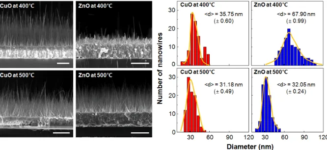
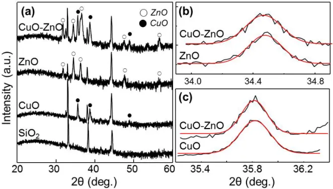
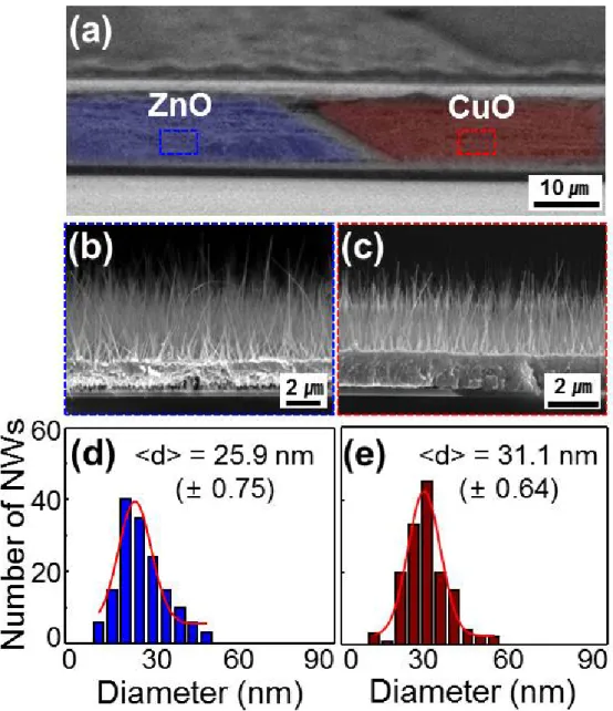
All the diffraction peaks can be indexed as a mixture of hexagonal and monoclinic phases, clearly indicating that the crystalline phases of ZnO and CuO are hexagonal and monoclinic phases, respectively58,59. The detailed crystal structures of the nanowires were investigated by low and high magnification TEM images of the nanowires. The diameters of the nanowires depend significantly on the average grain size in the grown films, determined by the film thickness and the growth temperature62.
To investigate the presence of impurity atoms in these materials, we have used micro-Raman spectra of ZnO-ZnO, CuO-CuO and ZnO-CuO samples in the range 0-1000 cm-1 at room temperature as shown in Figure 2.10 . However, there is no change in the position of the states and the presence of additional states, indicating that the no measurable doping with Zn (Cu) occurs in CuO (ZnO) nanowires. Depending on the compound types, the potential barrier height will be tuned and the adsorbate-induced change in height will be effectively modulated by the gases.
For CuO nanowires, the addition of H2 and CO gases to the air stream causes the source-drain current to decrease in less than 1 min, returning to its initial value reversibly when the reducing gases are turned off as shown in Fig. 2.12. For ZnO nanowires, only nitrogen dioxide gas reduces the source-drain current when the nanowire is exposed to the gas in Figure 2.12. Thus, this observed dependence of the gas responses of metal oxides based on the electronic properties of the material will be used to advantage to further improve the gas selectivity of the nanowire.
In the presence of a large number of H atoms, these hydroxyls can further react with H to create water, which can desorb, leaving an additional oxygen vacancy at the surface. The carbon dioxide also formed by the reaction of carbon monoxide and oxygen at the surface leaves an additional oxygen vacancy at the surface of the type 24. This resulted in the decrease of the downward (upward) band bending at the surface, leading to the increase (decrease) in the resistance of the nanowire, depending on the type of material.
As can be seen from Figure 2.12 (c), the radial plots of H2, CO and NO2 gas responses over the nanowire sensor are markedly different for two different materials (n-type and p-type).
CONCLUSIONS
EXPERIMENT
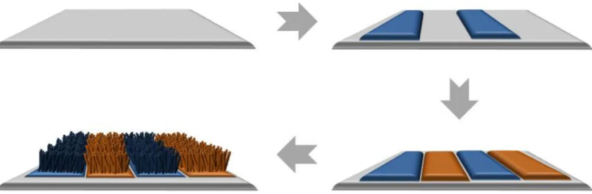
- Alternatively driven metal-oxide nanowires junctions
- Decoration of metal particles on nanowire junction arrays
- Response test of air-bridge-structured nanowire junction arrays toward H 2 , CO and NO 2 -
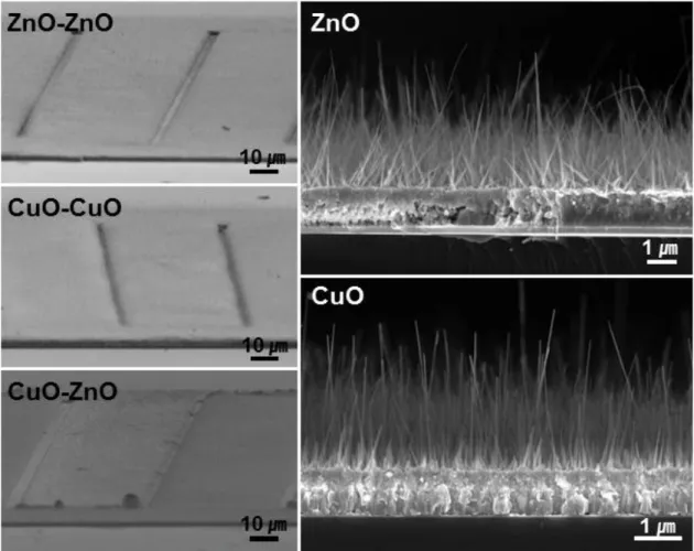
We adopted an Au electrode (~ . 200 nm) with Ti adhesion promotion layer (~ 20 nm) between the metal films and the substrate. Two-hour growth at 500oC typically results in nanowires ~ 10 µm long, long enough to bridge the 5 µm gap between the metal films (Figure 3.2). At lower temperature (673 K), the length of ZnO nanowires is not enough to bridge the 5 µm gap between the metal films and they show broad distributions in diameter.
SEM imaging indicates that in a typical synthesis, the nanowires cover the surface of patterned substrates uniformly and compactly and the average diameter is approximately 30 nm. After annealing at 473 K, the metal films aggregated into well-separated nanoparticles that uniformly covered the nanowire. Pristine and Ag-decorated junctions for e-nose sensor capability are also prepared on the substrate on which Pd-decorated sensors are placed.
The sensors were placed in a reaction chamber and exposed to pulses of one of three gases at different partial pressures introduced into dry air flowing at a rate of 2000 sccm: H2 (200 ppm), CO (200 ppm) and NO2 (200 ppm). Pulses of 200 ppm concentration gases balanced by dry air were introduced into the chamber under 1 atm of dry air background. Each of the analytes has a low moisture concentration of about 2.2x10⁻⁶ [µmol/mol] and the total hydrocarbon (THC) level is zero.
All three produced similar results and the linear discriminant analysis (LDA) of each yielded points located in approximately the same regions of parameter space for the three test gases. The results reported in this report were obtained in a long series of experiments of one of the devices.
RESULTS AND DISCUSSION
- Structured and morphology
- Electrical properties of nanowire junctions
- Gas sensing properties of air-bridge-structured nanowire junction arrays
- Linear Discriminant Analysis (LDA)
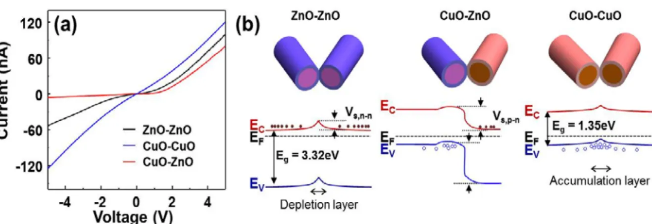
In contrast, this model may not be suitable to explain the I-V characteristics of the p-p junction. One of the three gases was periodically added to the continuously flowing air stream and then turned off. Representative values of the sensitivities of the sensor to the gases are given in Figure 3.5 (d).
The reactions will reduce the oxide from the electron donation from the molecule to the nanowire, so the electrons return to the interface of the overlapping nanowires, resulting in a decrease in the potential barrier and resistance of the sensor. On the contrary, the oxidizing gas (NO2) provides additional oxygen to the oxide, which increases the band bending upward in the surface region, leading to an increase in the sensor resistance23. When exposed to reducing gases, the chemisorption reducing gases will empty holes near the surface and reduce the thickness of the layer, resulting in an increase in resistance.
One process is probably a decrease in barrier height due to an increase in electron concentration due to electron donation from the molecule to the nanowire. Thus, adsorbate-induced Fermi level shifts are dominant for CuO materials, reducing the potential barrier height and reducing the sensor resistance. The second is probably a decrease in thickness in the p-side hole accumulation layer due to a decrease in oxygen concentration on the CuO surface, which increases the resistance.
Such two competing effects must be considered to explain the current response of the sensor. The total data set for the e-nose was processed using LDA and drawn as two-dimensional maps to indicate the extent to which the analysis can separate the response of the e-nose to the three gases into separate classes, as shown in Figure 3.9 . .
CONCLUSIONS
Discrimination between milk and cultured dairy products using screen-printed electrochemical arrays and an electronic nose. Large-scale fabrication of highly sensitive SnO< sub> 2 nanowire network gas sensors by single-step vapor phase growth. A near single crystalline TiO2 nanohelix array: improved gas sensing performance and its application as a monolithically integrated electronic nose.
Direct comparison of long-term performance< i> versus SnO< sub> 2 nanoparticle films. In situ observation of growth of ZnO nanowires on zinc film in environmental scanning electron microscopy. In situ monitoring of growth, interphase transformations, and patterning of single-crystal VO2 nanowires and nanoplatelets.
The synthesis of metal oxide nanowires by directly heating metal samples in a suitable oxygen atmosphere. Decoration of ZnO nanowires with Pt nanoparticles and their enhanced gas sensing and photocatalytic performance.