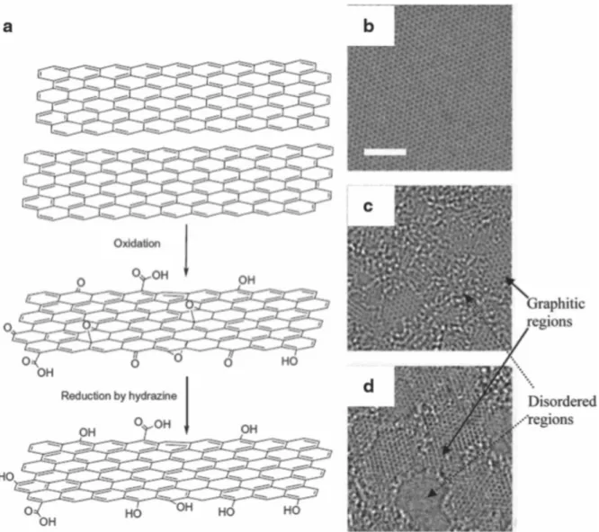
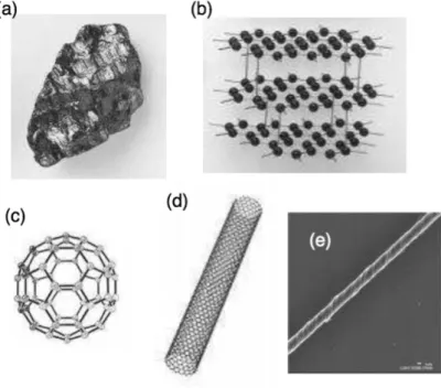
Reduction of graphene oxide (GO). a) Oxidation of graphite to GO and reduction to reduced graphene oxide (rGO)7. b) Hanging single sheet of graphene. The inset shows a magnified image of the high-frequency region. e) Capacity holding plot with cycle number. f) Schematic of recorded specific capacitances of EDLC electrodes obtained by different methods. First, I studied the way to make 3D graphene and lotus leaf-inspired 3D graphene using CVD methods and changing the surface of graphene with different transfer methods and used as SERS substrate.
Review
Graphene
- Introduction
- Electronic properties
- Mechanical properties of graphene
- Thermal properties
- Synthesis methods
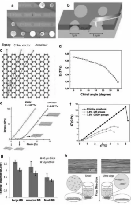
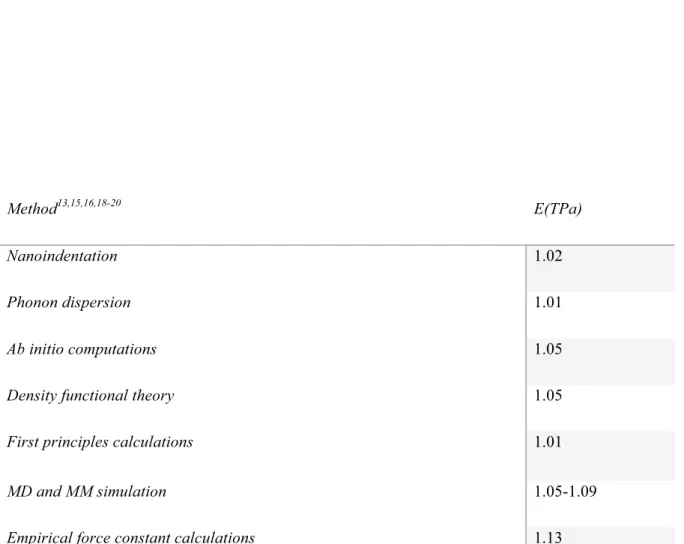
Many parameters have been reported to affect the Young's modulus of graphene, such as chirality, Young's chirality13, the presence of defects and wrinkles14, and functionalization15-16. This result, approved by the previous theoretical elastic properties of graphene, should be relatively independent of the orientation direction, so the chirality model should not affect the Young's modulus. The thermal properties of graphene lattice vibrations have attracted the interest of researchers in physics, chemistry, materials and engineering.
SERS
- Introduction
- Fundamental Aspects
- Chemical contributions
At this resonance state, the size of the surface plasmons is maximized and incoming light intensity is amplified and emitted. When the dimensions of the metal structure are less than the wavelength of incident light, the SPR is highly dependent on the geometry, size, proximity and composition of the nanostructures. When plasmon generation occurs at the nanoscale, the electron density of the entire structure will oscillate.
However, a direct interaction between the molecule and the underlying metal surface is not covered by this effect at all. In contrast, the CE mechanism is related to the electronic properties of the adsorbate and works by means of the increase in the electronic polarizability of the adsorbed molecule on the induced dipole thought; CE enhancements, of the order of one to three orders of magnitude, are significantly smaller than the EM contribution. First, charge transfer (CT) between the molecule in its electronic ground state and the metal can change the polarization of the molecule, leading to a change of the Raman scattering cross section of the molecule.
Second, the energy levels of the adsorbate molecule usually differ from those of the molecule in its unbound or "free" state. For example, let us assume that the laser excitation wavelength does not coincide with an electronic absorption band of the "free" molecule, but coincides with one of the adsorbed molecules. This is an integral component of the so-called CT resonance model, where the transition energies depend on the energy separation between molecular and metallic energy levels.
Electronic structure calculations on molecules in metal surfaces/aggregates are therefore an extremely valuable approach for investigating the role of the aforementioned contributions separately under controlled and a priori well-defined conditions. The interfacial structure of a metal group of molecules.
Superhydrophobic
- Fundamentals of superhydrophobic surface
- Superhydrophobic surface of graphene and graphene oxide
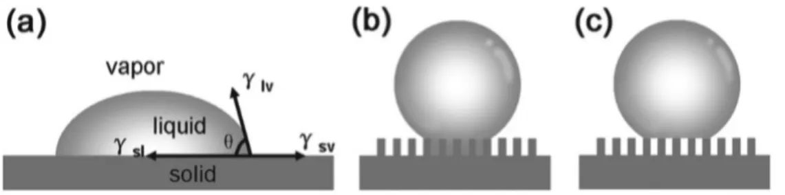
Surface wetting of graphene sheets plays a crucial role in determining their compatibility with the desired environment. So a deep understanding of the wettability of graphene and its related materials is fundamentally important for the development of graphene-based devices. Recently, several experimental and simulation studies have been focused on the surface properties and wettability of graphene films.
Quantum molecular dynamics simulations provide fundamental insight into the wetting behavior of water nanodroplets on a free-standing single-layer graphene sheet and also allow the incorporation of the polarization interaction, main-body effect and hydrogen bonding interactions in the prediction of the wetting ability. . Both theoretically and experimentally proven, graphene has a natural hydrophobicity, which is essential knowledge to understand the wetting behavior of water on the surface of such a material. In addition to pristine graphene, another important graphene-related material that has been widely used for the fabrication of graphene-based devices is GO.
GO is prepared by chemical exfoliation of natural graphite and can be considered as a derivative of graphene with oxygen functional groups on its basal planes and edges. The wettability of the GO film is affected by the OCG content on the surface. Invariably, GO shows hydrophilicity due to the chemical nature of the groups, such as carboxyl, hydroxyl and epoxy.
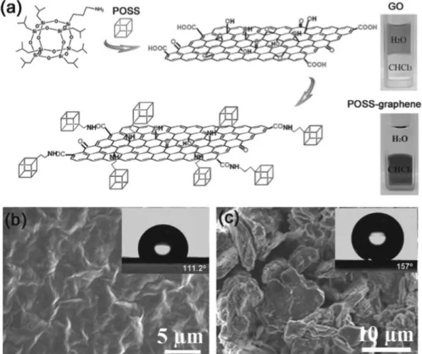
Drastic or partial removal of. a) Surface modification of GP with POSS, photographs of the original GO in water and the synthesized POSS_graphene in CHCl3.
Growth of large-area single- and double-layer graphene by controlled carbon deposition on polycrystalline Ni surfaces. Synthesis of a self-standing carbon nanohybrid with directly growing carbon nanotubes on air-sprayed graphene oxide paper and its application in a supercapacitor. Synthesis of three-dimensional reduced B-doped graphene oxide via supercritical fluid for oxygen reduction reaction.
Practical understanding and use of surface enhanced Raman scattering/surface enhanced resonance Raman scattering in chemical and biological analysis.
Three-Dimensional Graphene Nano-Networks with High Quality and Mass
- Introduction
- experimental methods
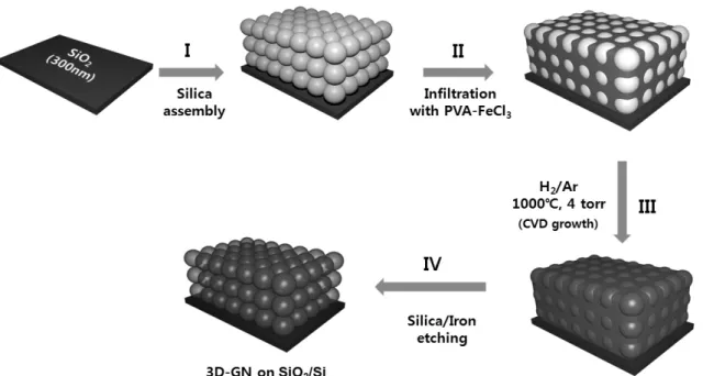
- Preparation of CS/PVA-FeCl3•6H2O composite thin film
- Fabrication of the 3D-GN
- Characterization of 3D-GN
- Electrochemical measurement
- Results and discussion
- Conclusions
- References
The superior performance of a 3D-GN as an electrode for supercapacitors is attributed to the realization of. To measure the conductivity of powder-type 3D-GN, the pellet with a diameter of 13 mm and a thickness of 50 m was prepared by mechanical grinding and subsequent pressurization (1000 kg/cm2) of 3D-GN. In addition to the formation of the network in the film, a bulk-scale of 3D-GN produced by solution drop-casting followed by CVD also gave a comparable quality of graphene (Raman, resistance, etc.).
The creation of graphene in 3D-GN can be verified by the decrease in the intensity of the D band and the development of sharp G and 2D bands at the higher frequency range. The dramatic increase in the intensity of the 2D band of 3D-GN at 350 phr indicates high quality of the single-layer graphene. Surprisingly, the average sheet resistance of 3D-GN obtained from more than 20 samples was 52 S/cm, which is close to the highest value recorded to date for a single layer of graphene.
Furthermore, the average sheet resistance of 3D-GN before iron removal was ∼50 Ω/□, implying potential for direct use of 3D-GN/iron as a porous 3D electrode. The best Raman spectrum, with a more enhanced 2D band and a lower D band, was obtained from the 3D GN grown on the sapphire substrate. As a demonstration of the potential of 3D-GNs, the performance of the 3D-GN sample as an EDLC electrode was investigated using cyclic voltammetry (CV) and galvanostatic charge/discharge measurements.
The 3D-GN was p-doped by being immersed in a HNO3 solution to further increase the conductivity up to 99 Ω/□. The significantly higher specific capacitance of 3D-GN compared to previously reported values for graphene electrode materials (101–282 F/g, as shown in Fig. 12f) can be attributed to the large accessible surface area achieved by appropriately sized mesopores and 3-dimensionally connected conductive graphene pathways. 3D-GNs can be grown on any inert substrate such as Al2O3, quartz or SiO2/Si wafer, etc.
Effect of the graphene transfer method on graphene -enhanced Raman
- Introduction
- Experimental methods
- Graphene growth and transfer process
- R6G dye adsorption on the graphene substrate
- GERS measurement
- Results and discussions
- Conclusion
- References
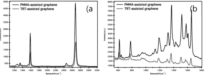
However, Figure 1b shows that all the GERS spectra peaks of the R6G probe on the PMMA graphene are higher than those on the more hole-doped TRT graphene. This observation is in disagreement with the above argument about GERS intensity based on the hole doping properties of graphene. COOH groups on the surface of the PMMA graphene are found to have twice the concentration of those on the TRT graphene, while the amount of epoxy/ether groups (C–O) is lower than that of the TRT graphene.
We can conclude that COOH or CO on the graphene surface affected the orientation of R6G and thus its π–π* interaction with the graphene surface35. In addition, the carboxyl groups, which are mostly located at the edges of the graphene surface, do not interfere with the π-π* stacking of R6G dye molecules on the graphene surface. On the other hand, the epoxy/ether groups located on the planar graphene surface tend to limit the π–π* interactions between the graphene surface and R6G.
Consequently, R6G molecules are preferentially positioned at C-C sites on the surface of a graphene that has a larger amount of COOH groups and less C-O groups. The arrangement of R6G molecules on the PMMA-graphene surface leads to strong π-π* interactions in the region where the epoxy/ether groups are absent. As a result, the density of R6G molecules on the surface of PMMA-graphene was higher than that of TRT-graphene, leading to a higher intensity of the UV absorption peak (Figure 15a) and more doping properties of holes (Figure 15b).
Probing the effect of molecular orientation on chemical enhancement intensity with graphene-enhanced Raman spectroscopy.
- Introduction
- Experimental methods
- Synthesis of CuO
- Chemical Vapor Deposition of Graphene on 3D Cu
- Transfer of Graphene
- Characterizations
- Conclusions
- References
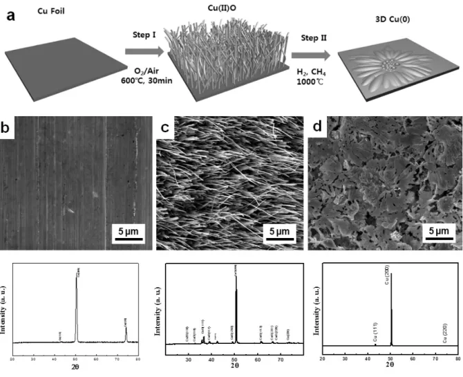
The morphology of the samples was characterized by Field Emission SEM (Nova Nano-SEM 230, 15 kV). The sheet resistances of the samples transferred on Si wafer were characterized by 4 point probe (Dasol Eng, FPP-RS8, pin spacing 1 mm, pin radius 100 m). It has been reported that the diameter and height of the nanowhiskers can be controlled by the annealing conditions.
Figures 1b-1d show SEM images of copper foil at each oxidation state and corresponding XRD results of the samples above. It is known that the graphene is nanostructured according to the surface morphology of the underlying copper during the growth process. As a result, the CVD-grown graphene on the Cu frame has a characteristic 3D nature of the lateral dimension in the order of tens of micrometers, as shown in Figures 18(a)–18(c) .
Therefore, we aimed to fabricate a dual-scale (micro- and nano-) graphene structure with a similar range of length scales to that of the lotus leaf by controlling the oxidation and reduction conditions. Interestingly, despite the coverage of the hydrophobic graphene film, the contact angle of the graphene/Cu film (d) does not show a noticeable increase compared to that of the pristine Cu film (c). The contact angle of a water droplet on the surface of 3D graphene on the PDMS substrate is up to 170o, much larger than that of the control sample (flat bare PDMS, g) (120o) and the lotus leaf (150o) .
After heat treatment or chemical modification of the surface by silane treatment, the surface of the lotus leaf-like graphene structure again became apparently superhydrophobic with a contact angle of 170, whereas the corresponding values of PDMS are 150.