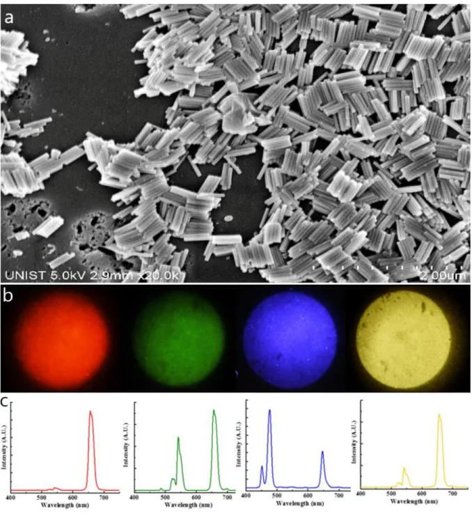
Microstructure array of each color was fabricated from UV-PDMS with silica-coated UCNs by DMD-based lithography.. color microstructure array fabrication procedure where the concentration balance of silica-coated UCNs is not controlled. Microstructure array was fabricated from UV-PDMS with silica-coated UCNs by DMD-based lithography. Color microstructure array fabrication method in which the concentration balance of silica-coated UCNs is controlled. Microstructure array was made of UV-PDMS with silica-coated UCNs by DMD-based lithography.. color microstructure array film. a) Optical image of 4-color microstructure array taken under 980 nm continuous wave laser.
Microstructure array fabrication techniques
In this way, commercial photocurable resins were tested and used to prove the usability of our systems in the photolithography technique. To investigate different monomer chemistries, we prepared conventional photocurable resins such as hydrophobic poly(urethane) acrylate (PUA), hydrophilic poly(ethylene glycol) diacrylate (PEGDA), 1,6-hexanediol diacrylate (HDDA). In this article, we discuss the physical and optical properties of these photocurable resins and the usefulness of each method.
Upconverting Nanocrystals (UCNs)
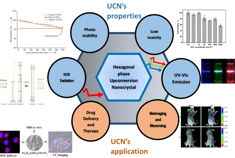
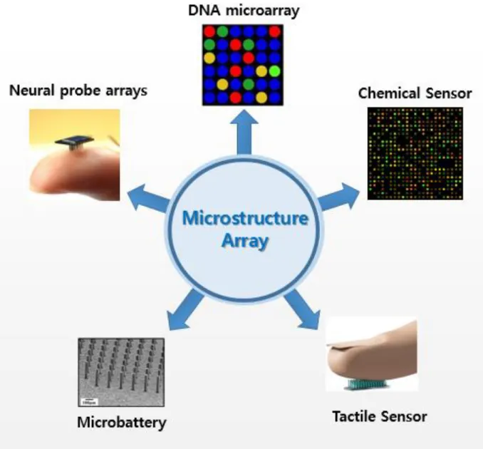
As the crystalline surface is covered with hydrophobic oleic acid, it results in the hydrophobicity of UCN. Overview of applications of microstructured arrays in various sectors, from DNA microarrays to tactile sensors, chemical sensors, microbatteries and neural probe arrays. A review of the properties of UCNs and the applications of UCNs in various sectors, from bioimaging to therapeutics and bioassays.
Microstructure array fabrication
Microstructure array fabrication using molding technique
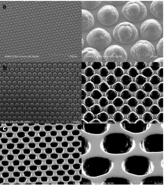
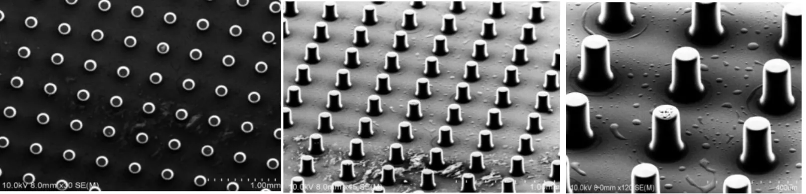
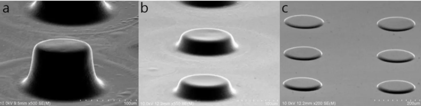
Microdome structure array with a diameter of (a) 100um, (b) 45um was made of PDMS. c) Replica mold with a diameter of 45um was made of PDMS. The disadvantage of the casting technique is that the mold must be produced with the conventional lithography technique when a new pattern is needed. The characteristic of the casting technique is also that the microstructure and the substrate are made of the same material.
Microstructure array fabrication using Digital micromirror device (DMD)
- Micropost array fabrication
- Microdome array fabrication
- Limitation of Microarray fabrication using DMD
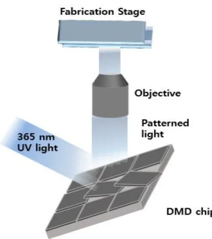
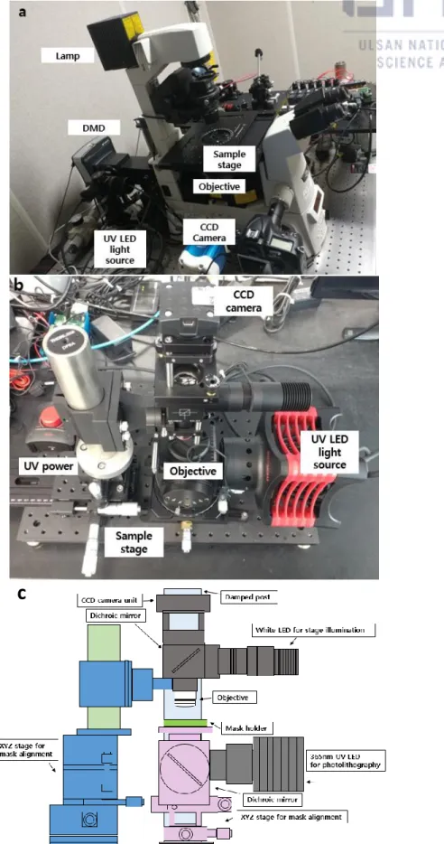
It can also be used to duplicate three-dimensional structures in a single step, while conventional photolithography is unable to replicate such structures. After fabricating the microstructure array stage, we inject UV-curable PDMS42 onto the stage, then expose 365 nm UV to the UV-curable resin using the DMD-based lithography system (Figure 7). By adopting the DMD-based lithography system, various structures can be made using photocuring resin.
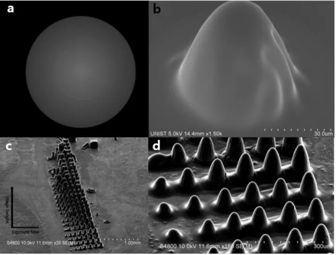
Since the DMD-based lithography system can change the projection pattern, grayscale projection is also possible in the lithography system. By adjusting the brightness of the grayscale lithography, we can control the fine shape of the structure. Since the photocurable resin hardens as much as the light passes through, a domed structure can be created depending on the amount of graduated light (Figure 9(b)).
By selecting any desired gradient via grayscale lithography, we can fabricate any desired structure. By adjusting the light exposure time and focal point of light, we can precisely control the shape of the structure (Figure 9(c), 9(d)). Even if the height of the stage is fixed, the height of the structure does not grow with the height of the stage.
Placing the focus of the light where it is also changes the fabricated structure.
Microstructure array fabrication using Contact lithography
- Microstructure array stage fabrication
- UV exposure using Contact Lithography
- PUA- UV exposure using Contact Lithography
- PEGDA- UV exposure using Contact Lithography
- HDDA- UV exposure using Contact Lithography
- PU- UV exposure using Contact Lithography
It can be seen that the height of fabricated structures is quite different depending on position in PDMS substrate. By reducing the height of the structure, the durability of the microstructure array during separation of the PDMS film from the glass can be significantly increased. It can be solved by reducing the height, and this results in reducing the load on the structure.
After UV curing, the Topglass with PDMS substrate is removed from the stage, and then the substrate is washed with ethanol (Figure 13(a)). After UV curing, the Topglass with PDMS substrate is removed from the stage, and then the substrate is washed with ethanol (Figure 13(b)). After UV curing, the Topglass with PDMS substrate is removed from the stage, and then the substrate is washed with ethanol.
This flexible PU resin also has urethane linkages with PTH as the primary chains, and it has acrylate reactive groups on both ends so that it can be used in photolithography. Figure (e) and Figure (f) show microstructure distribution when upper glass that is heated at high amp. covered, be used. Because it has characteristics of flexibility and elongation, this resin can be used in different ways.
After UV curing, the top glass with PDMS substrate is removed from the stage, then the substrate is washed with ethanol, and microstructure array can be obtained.
Microstructure array – mechanical property
The continuous urethane bonds form a long polymer network, resulting in an excessively high viscosity that makes it difficult to use in lithography. Because the low molecular weight and wide polydispersity of the resin can reduce its viscosity, and the low molecular weight chains can be used as diluents, the reaction is allowed to proceed at a low temperature of 60 °C to form a polymer with low molecular weight and wide polydispersity, which requires handling low viscosity (Figure 15 (a)). This resin cures with UV rays at high speed and has flexibility and elongation characteristics as it becomes cross-linked.
Because this resin has high viscosity and there is a limit for reducing the viscosity by controlling the reaction temperature, we must use this by mixing other photocurable resins. To fabricate the PU blend structure on a PDMS substrate, PU is mixed with each resin and photoinitiator. When flexible PU resin was mixed with PEGDA, large pores were formed in the structure (Figure 16 (b)).
When flexible PU resin was mixed with PUA, microstructures were easily damaged as PUA is a high modulus resin which leads to modulus difference between PDMS substrate. a) GPC data of flexible PU, Elongation property of flexible PU. Endurance varies from microstructure array depending on modulus of resin. a) PUA structure is easily damaged by stress due to its modulus difference between PDMS substrate.

UCN based Microstructure array fabrication
UCN synthesis
UCN surface modification and dispersion in photocurable resin
- UCN dispersion in hydrophobic PUA
- UCN oxidation and dispersion in hydrophilic PEGDA
- UCN oxidation
- Oxidized UCN dispersion in hydrophilic PEGDA
- UCN silica coating and dispersion in flexible PUA
- UCN silica coating
- Silica coated UCNs dispersion in PU
UCN-dispersed solution is injected into the fabricated microstructure array stage, then UV is exposed to the stage-containing solution. If normal UCN is used at this time, the UCN is not washed well, and it is difficult to obtain a clean microstructure array (Figure 21(a)). Because non-specific nanoparticles are accumulated over the stage, it is difficult to construct microstructure array using oil-coated UCNs.
In the case of a microstructure array with different colors, this should be avoided because the colors are mixed (Figure 21(b)). After all steps, PDMS film containing a microstructure array dispersed with multicolor UCNs can be obtained. Nonspecific binding of oleic acid-capped UCNs with PDMS substrate disrupts the clear distribution of (a) green microstructure array.
The microstructure array of each color was made of UV-PDMS with silica-coated UCNs by DMD-based lithography. Images taken under a 980 nm continuous wave laser. .. fabrication procedure for a color microstructure array where the concentration balance of silica-coated UCNs is not controlled. The microstructure array was fabricated from UV-PDMS with silica-coated UCNs by DMD-based lithography.
Images taken under a 980 nm continuous wave laser. .. fabrication procedure for color microstructure arrays controlling the concentration balance of silica-coated UCNs. Images taken under a 980 nm continuous wave laser. Array film with color microstructure. a) Optical image of a 4-color microstructure array taken under a 980 nm continuous wave laser. By adding UCNs, we could create a new concept of microstructure array that responds to near-infrared radiation.
UV exposure using Contact Lithography
- PEGDA- UV exposure using Contact Lithography
- PU- UV exposure using Contact Lithography
Conclusion
To find optimal resin, several commercial photocurable resins such as HDDA, PUA and PEGDA were used and approved for use in each method. Because it is a type of microstructure array that can immediately respond to near-infrared rays, it is expected to be applied in various ways such as sensor or optical equipment.
Experimental section
- UV-PDMS synthesis
- flexible PU synthesis
- UCN synthesis
- UCN surface modification
- UCN oxidation
- UCN silica coating
- microstructure array stage fabrication
- PDMS Spin coating onto substrate
- Spacer fabrication
- Top glass fabrication
- Surface acrylation
제가 졸업하는 동안 많은 도움을 주신 많은 분들께 진심으로 감사의 말씀을 전하고 싶습니다. 먼저, 아무것도 모르는 저를 가르쳐주시고 부족함과 서투름에도 불구하고 끝까지 이끌어주신 지도교수 이지석 교수님에게 진심으로 감사의 말씀을 전하고 싶습니다. 항상 교수님께 죄송하고 감사한 마음을 갖고 있습니다.
여러분이 주신 조언을 바탕으로 졸업 후에도 더 나은 사람이 되도록 노력하겠습니다. 또한, 논문심사를 위해 시간을 내어 주신 고현협 교수님, 이창영 교수님에게도 진심으로 감사드립니다. 구연발표와 인터뷰를 통해 저에게 베풀어주신 아낌없는 조언을 결코 잊지 못할 것입니다.
잊지 못할 연구실 구성원 모두에게 감사드립니다. 늘 부재중이었던 늙은이, 청년이었는데도 끝까지 응원해주셔서 진심으로 감사드립니다. 정말 고마운 것들이 너무 많아서 다 열거하기 힘들고 좋은 추억으로 남아 있어서 정말 감사해요.
앞으로도 더 열심히 노력해서 자랑스러운 소년이 되도록 하겠습니다.