I certify that this project report titled “NOVEL TWO-WAY FILTER AND DIPLEXER” by LEE YAN MING has met the required submission standards and partially met the requirements for the award of the Bachelor of Electronics and Communication Engineering (Hons.) at the University Tunku Abdul Rahman. The use of any material contained in or derived from this report must always be duly acknowledged.
Background
Research Aim and Objectives
In the second idea of this project, a low-pass and band-pass diplexer was proposed and designed. But unlike the first idea; there is only a single input port and two output ports which are frequency dependent.
Project Motivation
Throughout this project, many reference books and journals were referred to in order to gain a better understanding of the theories and design parameters of microwave filters.
Thesis Overview
Background
Microwave Filters
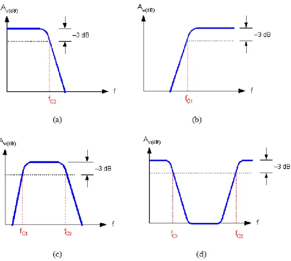
Filter Parameters
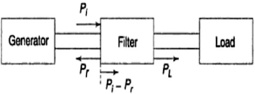
Pi is the incident power, Pr is the reflected power and PL is the power supplied to the load. From the Amplitude response, the most important parameters are insertion loss and return loss (Das and Das 2001).
The Effect of Mismatch
An impedance mismatch will result in a reflection of signals at the ports and thus, affect the performance of the filter (Das and Das 2001).
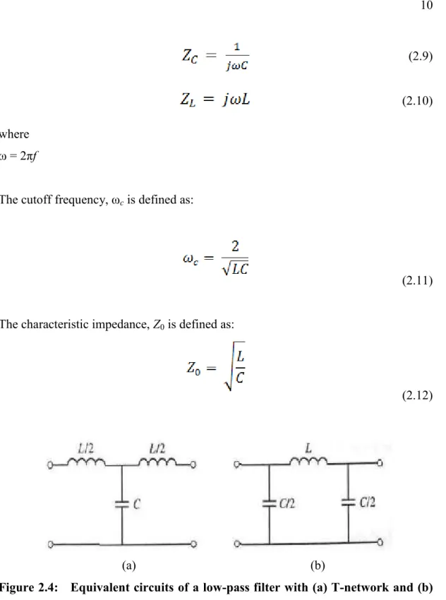
Low-pass and High-pass Filters using LC Elements
The high-pass filter allows high-frequency signals to pass through while blocking low-frequency signals (Pozar 1998).
Recent Developments
Miniaturized Filters and Diplexers
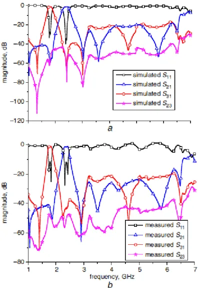
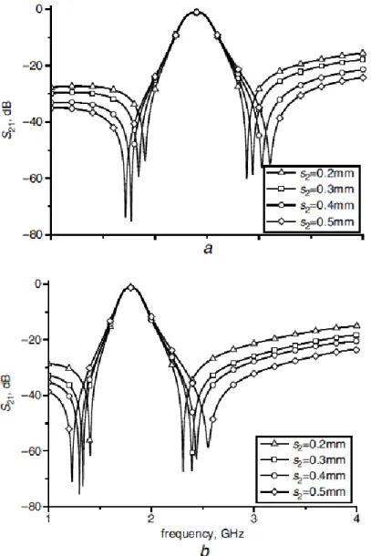
The authors managed to reduce the size of the diplexer by combining bandpass filters without the need for a matching network (Zayniyev, Budimir et al. 2008). The following Figure 2.8 and Figure 2.9 show that the experimental results of the fabricated microstrip are in good agreement with the simulated results (Zayniyev, Budimir et al. 2008).
Such a property allows the improvement of the isolation between the two channels (F.Cheng, Lin et al. 2012). The simulated and measured results of the diplexer are thus in good agreement (F.Cheng, Lin et al. 2012).
High Selectivity Dual-band Bandpass Filter
Shi proposed a compact microstip-line dual-band bandpass filter using folded impedance resonators with high selectivity.
Research Methodologies
The Simulation Stage
In this phase the softwares TX Line and Ansoft HFSS (High Frequency Structure Simulator) were used. Prior to the design and simulation process, TX Line was used to calculate the width of a 50 ohm feed line based on the design specifications. Ansoft HFSS uses the Finite Element Method (FEM) with adaptive meshing to solve the simulation process.
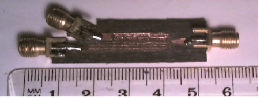
Fabrication Stage
Experiment Stage
A software called Freelance Graphics is used to compare and analyze the simulated and measured results.
Background
Two-way Low-pass and High-pass Filter
Configuration
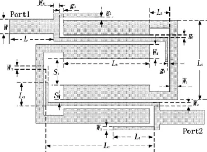
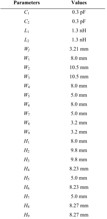
This proposed design is fabricated on a Duroid RO4003C substrate (with a dielectric constant of r = 3.38 and a thickness of 1.524 mm). Basically, the proposed design is a four-gate filter consisting of low-pass and high-pass filters. For the high-pass filter, Port 3 serves as an input port while Port 4 serves as an output port.
The middle patch of the proposed filter is connected to a pair of inductors and a pair of capacitors. The trip path with a pair of inductors functions as a low-pass filter while the trip path with a pair of capacitors functions as a high-pass filter.
Simulation and Experiment Results
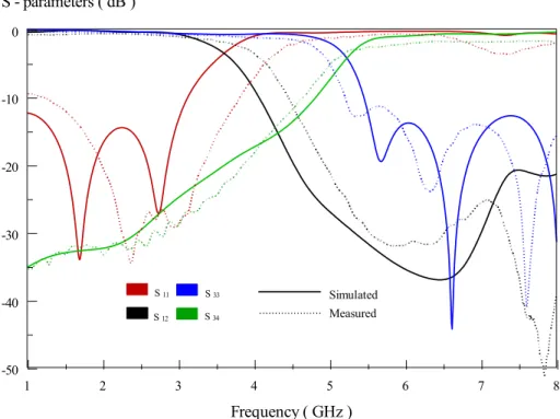
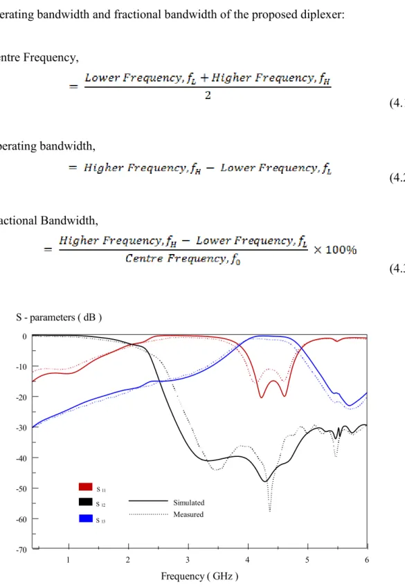
In the simulation, the insertion losses for the low-pass and high-pass filters are -0.18 dB and -0.45 dB, respectively. The low-pass filter has a 3 dB cut-off frequency of 3.55 GHz, while the high-pass filter has a 3 dB cut-off frequency of 5.3 GHz. The simulated result shows that the passbands of the low-pass and high-pass filters have a return loss of less than -10 dB within their bandwidth.
The measured turn-on losses for the low-pass and high-pass filters are -0.65 dB and -1.72 dB, respectively. Measurements of the fabricated design show that the 3 dB cut-off frequency of the low-pass filter is 4.01 GHz, while the high-pass filter has a 3 dB cut-off frequency of 5.05 GHz. Measured return loss from the high-pass filter remains below -10dB, but the return loss for the low-pass filter is in the range of 1.00 GHz to 1.18 GHz.
All these factors will cause a discrepancy in the cutoff frequency between the simulated and measured results. The low-pass filter has a 3-dB cut-off frequency error of 12.96%, whereas the high-pass filter has a 3-dB cut-off frequency error of only 4.72%.
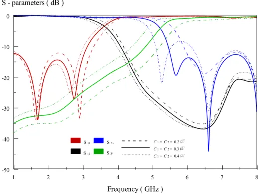
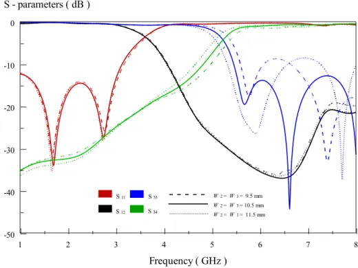
Parametric Analysis
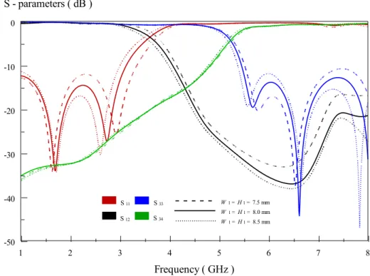
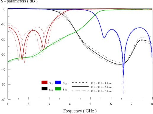
The significant changes can be seen in the 3-dB cut-off frequency and the return loss of the low-pass filter. When W1 and H1 are increased to 8.5 mm, the return loss of the low-pass filter decreases. Significant effect on the 3-dB cutoff frequency and return loss of the high-pass filter is shown in Figure 3.19.
The return loss of the low-pass filter changes significantly as the parameters vary. The return loss is affected by ±1 dB and the poles of the low pass filter are shifted as the parameters vary. Similarly, the changes in W1 also have a drastic effect on the return loss of the high-pass filter.
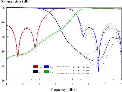
There is also a slight shift in the 3 dB cutoff frequency of the low-pass filter. The significant effect on the return loss of the high-pass filter is shown in Figure 3.19. This is because the parameter W2 is in the motion path of the high-pass filter.
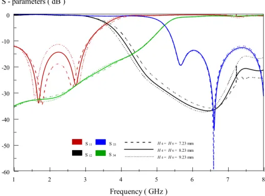
Increasing and decreasing the value of W4 affects the return loss of the low-pass filter by ±1 dB.
Discussion
The electric fields of the low-pass filter at 1.69 GHz with different phases can be observed in Figure 3.25. Similarly, Figure 3.26 shows the traveling electric field of a low-pass filter at 2.75 GHz as the phase changes. In addition, the electric field strength at the input terminal is similar to the output terminal, since signals can flow through low-impedance inductors of 1.3 nH.
Therefore, most of the input signals are being transmitted to the output port and thus, causing the filter to have very low return loss at the input port. Most of the input signals from Port 3 are being transmitted to Port 4 since the 0.3 pF capacitors have low resistance when operating at high frequencies. This can be clearly seen as the electric fields at the input and output ports are of the same intensity.
The low-pass and two-pass filter electric fields at 4.3 GHz were captured as shown in Figure 3.29. Additionally, most signals are reflected back to the input ports, causing the return loss to be close to 0dB.
Background
Low-pass and Bandpass Diplexer
Configuration
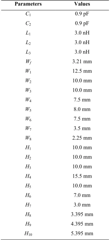
The proposed design of a low-pass and band-pass diplexer was designed and fabricated on a Duroid RO4003C substrate (with a dielectric constant of r = 3.38 and a thickness of 1.524 mm). In the design, port 1 is the input port, while port 2 and port 3 are the output ports. Based on calculation, this is achieved by designing each feed line to have a width of 3.21 mm.
On the other hand, a longer travel path that serves as a low-pass filter is connected to the inductors.
Simulation and Experiment Results
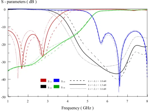
In the simulation, the insertion losses for the low-pass and band-pass filters are -0.12 dB and -0.43 dB respectively. The low-pass filter has a 3-dB cutoff frequency of 2.05 GHz, while the band-pass filter has a center frequency of 4.415 GHz. In addition, both the low-pass and band-pass filter have a return loss of less than -10 dB within its bandwidth.
From the experiment, the measured insertion losses for the low-pass and band-pass filter are -0.44 dB and -1.37 dB, respectively. Measurements from the fabricated design show that the 3-dB cutoff frequency of the low-pass filter is 2.03 GHz, while the band-pass filter has a center frequency of 4.35 GHz. The operating passband of the bandpass filter is from 3.99 GHz to 4.71 GHz, which comes to a total bandwidth of 720 MHz.
There are some minor shifts in the bandwidth of the low-pass filter and the band-pass filter. The low-pass filter has a 3-dB cutoff frequency error of only 0.98%, while the bandpass filter has a center frequency error of only 1.47%.
Parametric Analysis
The significant changes can be seen in the stripping of the low pass filter. As the W1 parameter is changed, the amplitude response of the bandpass filter is affected. Since H1 lies within the bandpass filter drive path, the lowpass filter is therefore unaffected by the changes.
Reducing W3 to 8.0 mm causes the S11 to split into two poles at the low-pass filter and increases the return loss of the band-pass filter. Significant effect on the amplitude response of the low-pass and band-pass filters can be observed in Figure 4.11. In addition, the 3-dB cutoff frequency of the low-pass filter shifts to 1.87 GHz and a narrower bandwidth is obtained at the band-pass filter.
Changing the parameter H5 only affects the amplitude response of the low-pass filter, since H5 is part of the travel path of the low-pass filter. Changing the values of H6 has an effect on the return loss of the low pass filter.
Disccussion
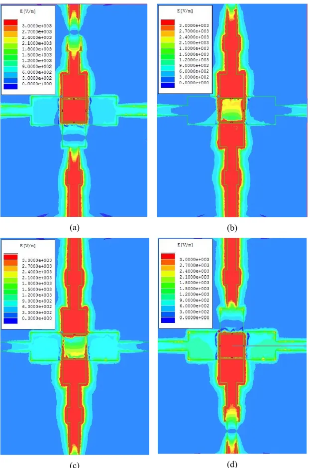
The electric fields in the low-pass filter at 1.07 GHz with different phases can be observed in Figure 4.19. Furthermore, the electric fields at the input port have the same intensity as the electric fields at the output ports. Previous equations have proven that the capacitors have high impedance at low frequencies and therefore most of the signals are blocked.
Most of the input signals from port 3 are transmitted to port 4, since the 0.9 pF capacitors have low impedance when operating at high frequencies. This can be clearly seen since the strength of the electric field at the input and output ports is of the same intensity. On the other hand, there are no signals propagating towards port 2 due to the presence of the 3.0 nH inductor.
The electric fields of the proposed diplexer at 4.3 GHz were captured as shown in Figure 4.22. Additionally, most signals are reflected back to the input port, causing the return loss to be close to 0dB.
Achievements
Future Work
Conclusion
High-Selectivity Dual-Band Bandpass Filter Using Folded Stepped Impedance Resonators and Asymmetric Coupling Lines.