I declare that this report entitled “MEMORY SYSTEM DESIGN AND DEVELOPMENT FOR RISC 32-BIT 5-PHASE CELLS: MEMORY SYSTEMS INTEGRATION” is my own work except for those mentioned in the references. Mok Kai Ming, who encourages me when I've lost faith, comforts me when I'm stressed, and enlightens me when I've lost my way. A million thanks and appreciation for his guidance and wisdom throughout the course of this project.
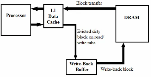
This project is to improve the current RISC32 architecture developed in Universiti Tunku Abdul Rahman under the Faculty of Information and Communication Technology by redesigning the memory system. After reviewing the previous work, use the RISC32 processor memory system cache unit with write-through scheme which can improve its efficiency more. Therefore, this project is initiated to redesign the cache unit into write-back cache and add a write buffer (FIFO) in the cache unit to handle the data transferred to SDRAM when read misses and write misses occur.
Some modifications on memory arbiter have been done so that the new cache unit works in the memory system. This project is modeled using Verilog HDL and a test program will be developed to test the functionality and compatibility of the newly designed write-back cache with the rest of memory system (memory arbiter, SDRAM controller, SDRAM).
Introduction
Background Information
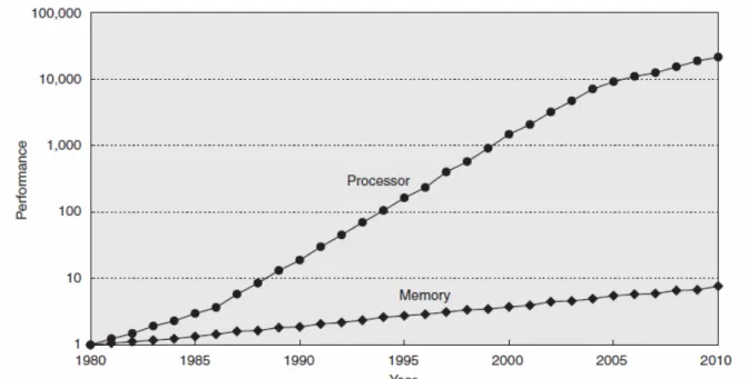
Faculty of Information and Communication Technology (Perak Campus), UTAR Page 12. Memory hierarchy was introduced in the late 1960s to reduce average latency and reduce the bandwidth required to speed up the memory system. The performance of a memory hierarchy analysis via the average memory access time, using the following expression:. average memory access time = hit time + miss rate * miss penalty. Thus, the effort to reduce the performance gap between the processor and physical memory is concentrated on efficient implementations of a memory hierarchy to reduce misses, mispenalty, and hit time.
Motivation and Problem Background
Memory hierarchy was introduced in the late sixties to provide lower average latency and reduced bandwidth requirements to speed up the memory system. The lack of well-developed verification specifications for these microprocessor cores will certainly affect the physical design phase. Otherwise, if the front-end design requires change, the entire physical design must be redone.
Problem Statement
Literature Review
- Write-through Scheme vs Write-back Scheme
- Write buffer
- Write Buffer Saturation
- Write-back Scheme with Write Buffer
- Reduce Miss Rate via Larger Block Size: Multiword Block Direct Mapped Cache
- Cache Unit
- Cache Associative
- Scenarios to Represent Cache Behaviours
- Block Partitioning of Cache Unit
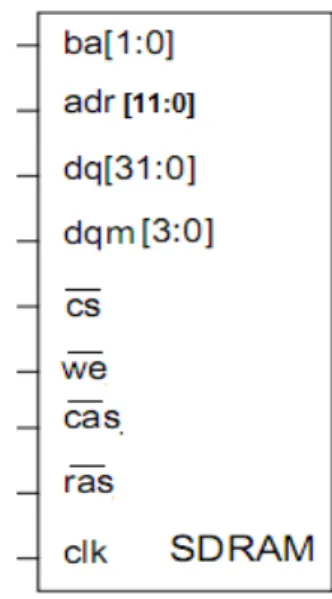
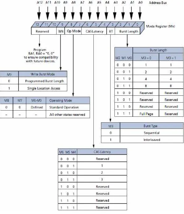
- SDRAM
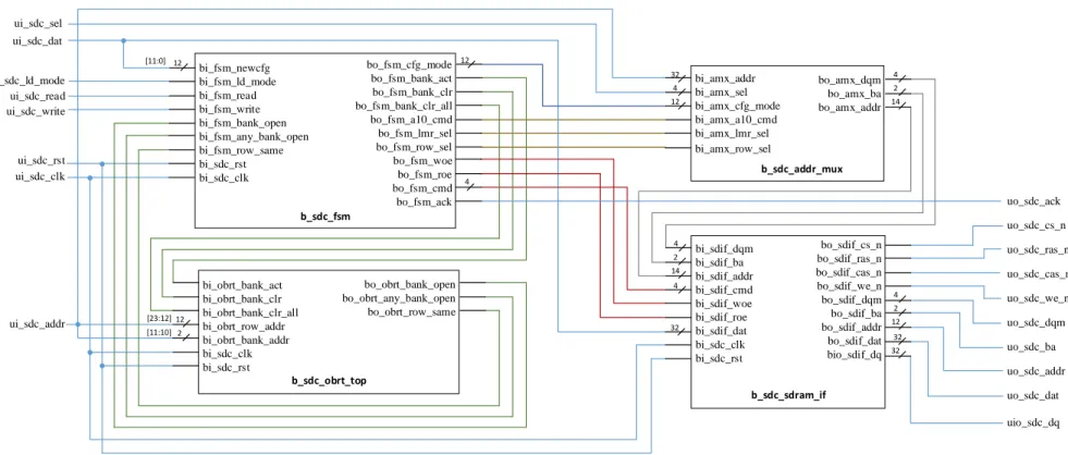
- SDRAM Controller
- Block partitioning of SDRAM Controller
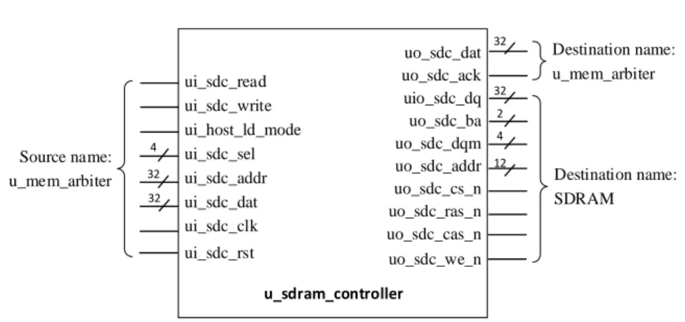
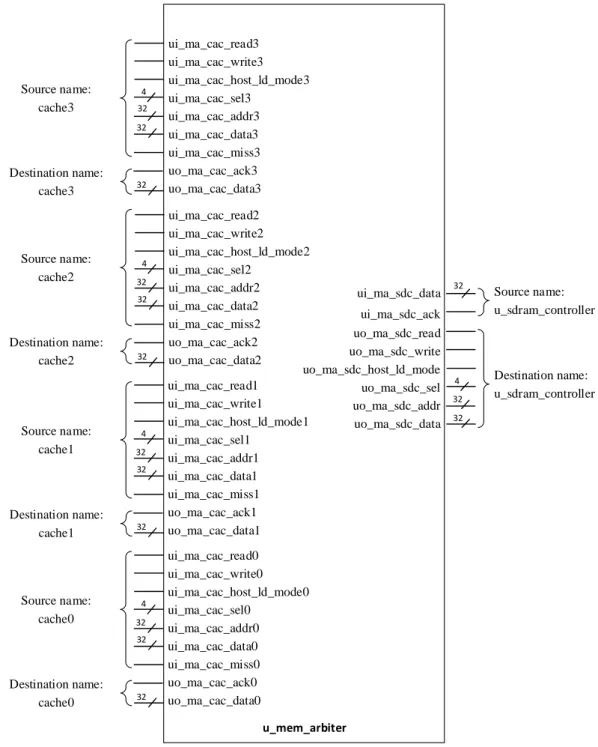
- Memory Arbiter
- I/O Description
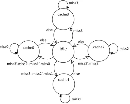
- Memory Arbiter State Diagram
- State Definition
- Output or Behaviors Corresponding to the States
The memory controller asserts strobe, cycle, and read signals to the SDRAM controller to receive new data. The memory controller asserts strobe, cycle, and read to the SDRAM controller to access the data in the SDRAM. SDRAM control by the SDRAM controller modeled by Chin Chun Lek, so in this project it is enough to focus on the function of SDRAM and its configuration – determining the load mode.
32. ui_sdc_read ui_sdc_write ui_host_ld_mode ui_sdc_sel ui_sdc_addr ui_sdc_dat ui_sdc_clk ui_sdc_rst. uo_sdc_dat uo_sdc_ack uio_sdc_dq uo_sdc_ba uo_sdc_dqm uo_sdc_addr uo_sdc_cs_n uo_sdc_ras_n uo_sdc_cas_n uo_sdc_we_n u_sdram_controller.
Project Scope and Objectives
Project Objectives
Impact and Significance
Method and Technologies Involved
Design Methodology
- Micro-architecture Level Design (Unit Level)
- Micro-architecture Level Design (Block Level)
This project was only involved in micro-architecture level design (Unit level and Block level) as higher architecture level was complete and only waiting for integration. The unit module is divided into several blocks that each block has its own functionality to perform the sub-function of the unit module to reduce complexity of design process. Once finished with the micro-architecture specification, with the information in the specification, RTL modeling with High Level Language or Hardware Description Language (HDL) can be started.
Verilog will be used as design language in this project during RTL modelling. The model must then go through a verification process that verifies the functionality of the design that must conform to the microarchitecture specification.
Design Tools
- Verilog HDL Simulator - Mentor Graphics ModelSim SE-64 10.1c
Memory System Specification
Partitioning and Design Hierarchy
Memory System Specifications
Memory Map
Architecture of Memory System
Micro-Architecture Specification
Cache Unit
Scenarios to Represent Cache Behaviors ............................Error! Bookmark not defined
Block Partitioning of Cache Unit
Cache Controller Block
- Cache Controller block I/O description
- Cache Controller State Diagram
- Cache Controller State Definition ................................Error! Bookmark not defined
- FIFO Controller block I/O description
- FIFO Controller State Diagram
- FIFO Controller State Definition..................................Error! Bookmark not defined
- FIFO Controller block I/O description
Verification
Test Plan
Testbench Verilog Code
Simulation Result
Cache_3 has priority to run first according to priority in the memory arbiter. The data was continuously written to the cache (the data became dirty because it is not updated on the SDRAM) and then the data for the next two clock cycles was read into uo_cac_cpu_data. A write miss occurred and FIFO_hit is invalidated because it tried to write to a cache location valid=0.
A write miss occurs and FIFO_hit is not asserted because the attempt to write to the cache location is different. Since the cache location to be written to is dirty, the block is fetched and copied to the FIFO. A write miss occurs and FIFO_hit is asserted because the attempt to write to the cache location is different.
The cache location to be written is dirty, so move the data block from the cache to the FIFO. The FIFO waits for the SDRAM to prepare the receive data, then when the ack signal is asserted, the data is written back to the SDRAM. While writing to SDRAM, a read error occurs, so the pipeline is blocked until the block of data is finished being written to.
Read miss and FIFO miss (fifo_hit de-asserted) happen because tag is different; data must be read back from SDRAM to cache and. Read miss because tag is different and fifo_hit asserted, data written back from FIFO to SDRAM. FIFO full, so FIFO writes data back to SDRAM first to free space, then continue the write miss process.
Conclusion
- Conclusion
- Discussion and Future Work
- Naming Convention
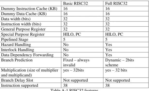
- Basic RISC32 processor
- Processor Interface
- I/O Pin Description
- System Register
- General Purpose Register
- Special Purpose Register
- Instruction Format
- Addressing Mode
- Instruction Set and Description
- Memory Map
- Operating Procedure
In Proceedings of the 3rd Internal Conference on Computer Architecture, Universidade do Minho http://gec.di.uminho.pt/discip/minf/ac0102/1600IRAM.pdf. Chin Chun Lek Bit Memory System Design: Design of Memory Controller for Micron SDR SDRAM” University of Tunku Abdul Rahman, Faculty of Information and Communication Technology. Ching Yi-lynn (2008) “Memory System Design: Integration of Caches, Translation Side Buffer (TLB) and SDRAM” Tunku Abdul Rahman University, Faculty of Information and Communication Technology.
Oon Zhi Kang (2008) “SDRAM Improvement: Designing the WISHBONE SDRAM Controller Industry Standard” Tunku Abdul Rahman University, Faculty of Information and Communication Technology. Type Pin type lower o : output i : input r : register w : wire f- : function level Name of the lower level all if, id, ex,. Based Displacement Addressing, where the operand is at a memory location whose address is the sum of a register and a constant in the instruction.
PC relative addressing, where branch address is the sum of the PC and a constant in the instruction. Pseudodirect addressing, where the jump address is the 26 bits of the instruction concatenated with the top bits of the PC.