Diploma thesis submitted in partial fulfillment of the requirements for a master's degree in engineering (electrical engineering and computer science). The examination board unanimously approved this thesis submitted by Mr. Jie Gan, in partial fulfillment of the requirements for the Master of Science in Electrical and Computer Engineering at Mahasarakham University. Mahasarakham University has approved acceptance of this assignment in partial fulfillment of the requirements for the Master of Science in Electrical and Computer Engineering.

- Industrial robots
- Service robots
- Military robots
- Medical robots
- Simulation robots
- Conventional charging mode
- Fast charging mode
- Battery replacement method
The charging method of the mobile robot depends on the battery performance and charging requirements. The advantage of the fast charging method is that the charging time is short, which can extend the life of the battery. Due to the fact that the volume and heat dissipation limitations of the power supply devices.
![Figure 2 TOP 5 applications for professional use [5]](https://thumb-ap.123doks.com/thumbv2/filepdfco/10213140.0/14.892.122.790.448.988/figure-2-5-applications-professional-use-5.webp)
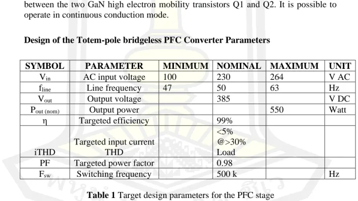
Boost PFC circuit control strategy
Boost PFC circuit has two control purposes: one is to make the output voltage stable, and the other is to make the power factor close to 1. The inductor current under CCM control is continuous, with small ripple and low THD, which is beneficial to the design of the filter inductor, while the output voltage swing is small and the output capacitor requirement is not high, but the CCM control structure is complex and requires measurement of both the grid voltage and the inductor current. BCM control is between CCM control and DCM control, but it generates a large current loop which causes the switch tube to be subjected to a large current load.
To meet the high power factor requirements of the power supply, the CCM control method with better overall performance should be selected.
LLC resonant converter control strategy
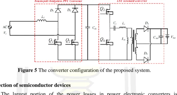
Considering power supply efficiency requirements, pulse frequency modulation (PFM) control is more suitable for fully resonant converters. Based on the above comparative selection of AC-DC converter and DC-DC converter respectively, the overall topology of the power supply can be obtained as shown in Figure 5. Most of the power losses in power electronic converters are dissipated in their power semiconductor devices.
Currently, these power devices are based on mature and well-established Si technology, although Si exhibits some significant limitations regarding blocking voltage capability, operating temperature, and switching frequency. Consequently, a new generation of power devices based on wide band gap (WBG) semiconductor materials for power converters is expected. The use of these new WBG power semiconductor devices will allow increasing the efficiency of power transformations by achieving a more rational use of power along with a significant improvement in the size and durability of power converters.
12 . frequencies), real commercial availability of the starting material (wafers and epitaxial layers) and maturity of their technological processes. The breakdown voltage of SiC and GaN is 10 times higher than that of Si, making them suitable for high voltage applications. SiC has higher thermal conductivity than both GaN and Si, making it more suitable for high-temperature, high-power applications.
Therefore, based on the principle of high efficiency, it is more appropriate to choose GaN devices.
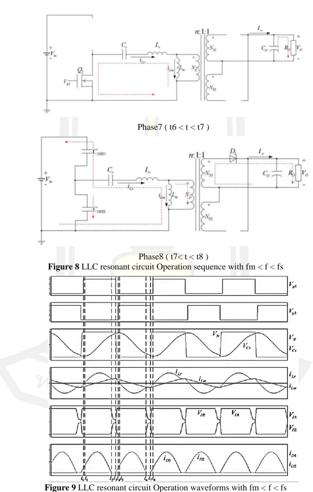
At the instant t1 the resonant current iLr rises to 0 and the phase 1 operating state ends. At the moment t2, the Lr current is equal to the Lm current and the phase 2 operating state ends, when the current of the output diode D1 becomes 0. At this time, the current in Lm is greater than the current in Lr, and the difference between them flows through the primary side of the transformer, and the rectifier diode D2 begins to conduct.
At t4, the discharge of Coss2 ends, and the body diode of Q2 turns on, at which point the phase 4 operating state ends. At this time, the rectifier diode D2 is on and the transformer primary voltage is clamped at -nVo, which is negative and positive. Lm is linearly charged at this voltage and does not participate in resonance, only Lr and Cr participate in resonance, and the resonant current flows through Lm and the primary side of the transformer and the body diode of Q2, and the energy is transferred to the output Vo.
At the instant t5, the resonant current iLr drops to 0 and the phase 5 operating condition ends. Only Lr and Cr participate in the resonance, and the resonant current flows through Lm and the primary side of the transformer, transferring energy to the output Vo. At t6, the Lr current is the same as the Lm current and the phase 6 operating condition ends when the current of the output diode D2 becomes 0.
Since the current in Lr is greater than the current in Lm, the difference between the two flows through the primary side of the transformer, and the rectifier diode D1 begins to conduct.
How it works when f = fs
At this time, the rectifier diode D2 is on and the transformer primary voltage is clamped to -nVo, with negative top and positive bottom. At t6, the current of inductor Lr and inductor Lm are equal, the rectifier diodes D1 and D2 are reverse biased and cut off, the output is isolated by a transformer and Lm begins to participate in resonance. The resonant current charges the parasitic capacitor Coss2 of Q2 and discharges the parasitic capacitor Coss1 of Q1.
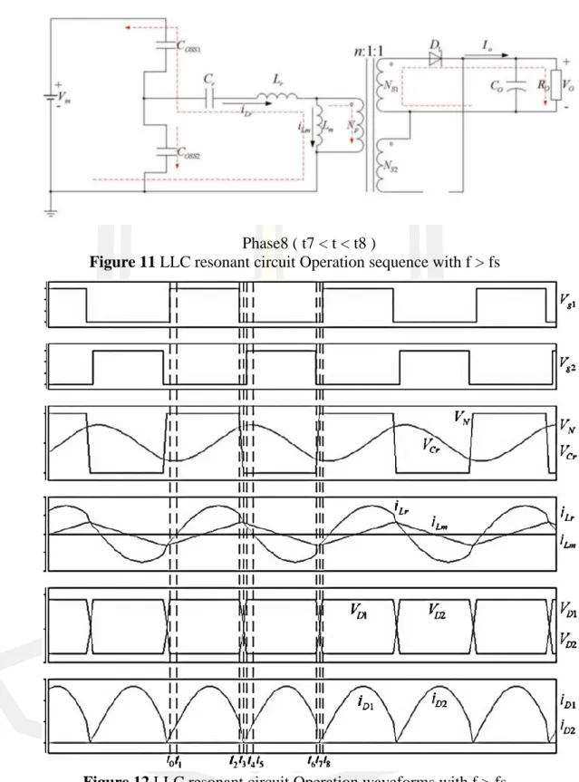
How it works when f > fs
This phase is similar to the one at fm < f < fs, where the current in the resonant inductor Lr flows through the body diode of Q1, creating the conditions for the ZVS conduction of Q1. Because the switching period is shorter than the resonant period of resonant capacitor Cr and resonant inductor Lr, when Q1 turns off, the resonant current has not yet completed half a cycle. Therefore, the current in Lr is greater than the current in Lm, and the difference flows through the primary side of the transformer, the rectifier diode D1 is still on, and Lm is clamped by the output voltage.
At this time iLr continues to decrease to less than iLm, the difference between the two flows through the primary side of the transformer, the polarity of the primary side of the transformer becomes negative and down to positive, the rectifier diode D2 starts to conduct, Lm is clamped by the output voltage. The work process of the last half-cycle converter is similar to that of the first half-cycle, so the work process of the subsequent half-cycle will not be described in detail. The required gain at the maximum and minimum input voltage can be determined using the following equations.
For an integrated transformer, the actual turns ratio of the transformer should be calculated using the following formula. The direct current characteristics of LLC resonant conversion are divided into zero voltage operating range and zero current operating range. When the input voltage drops, a higher gain can be achieved by reducing the operating frequency.
By choosing the appropriate resonance parameters, the LLC resonant converter can operate in the zero voltage operating region regardless of load changes or input voltage changes.
Comparison of the Outputs
Comparison of the Totem Pole bridgeless PFC circuit outputs, Figure 16 is the output voltage and current waveforms using the GaN HEMT device, Figure 17 is the output voltage and current waveform using the Si MOS device, it can be seen that the output of the Totem pole bridgeless PFC circuit using the GaN HEMT device is more stable. Comparison of LLC resonant circuit output, Figure 18 is the output voltage and current waveforms using GaN HEMT devices, Figure 19 is the output voltage and current waveforms using Si MOS devices, Vrms=48.795 V, Irms=10.589 A when GaN HEMT- devices are used, Vrms=48.74 V and Irms=10.577 A when Si MOS devices are used, it can be seen that the two types of output waveforms in the LLC resonant circuit are basically the same when the resonant frequency is not high. Comparison of Voltage and Current Voltage on Semiconductor Devices Figure 20 is the totem pole bridgeless PFC circuit GaN HEMT device voltage.
Comparison of Voltage and Current Stresses on Semiconductor Devices
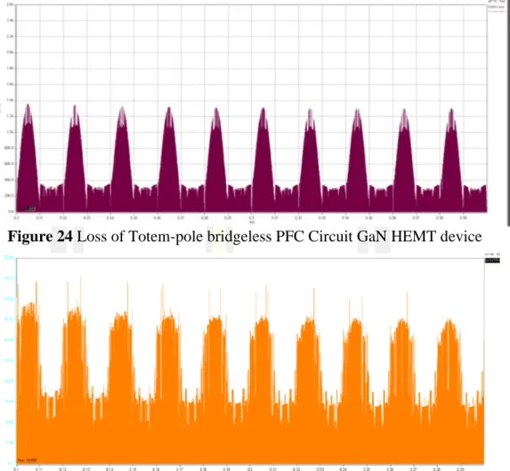
Semiconductor device loss comparison
When LLC uses GaN as the main switching device, its loss reduction effect is not as obvious as that of the PFC stage, mainly because LLC is a soft switching topology, and its switching loss is already very small. Compared to GaN devices, the Si used is MOS. The Rdson of the device is also 70mΩ. Therefore, compared to the PFC stage, the loss of the GaN HEMT device is only 63.5% lower than that of the Si MOS device.
Mattavelli, "GaN-baseret højfrekvent totempol-broløst PFC-design med digital implementering," i 2015 IEEE Applied Power Electronics Conference and Exposition (APEC), 15.-19. marts s. Mattavelli., "GaN-baseret højfrekvent totem-pole broløst PFC-design med digital implementering," i 2015 IEEE Applied Power Electronics Conference and Exposition (APEC), 15.-19. marts s. Costinett, "Investigation of Gallium Nitride devices benefits on LLC resonant DC-DC converter," i 2015 IEEE Applied Power Electronics Conference and Exposition (APEC), 15.-19. marts s.
Zhang, “Investigation of cascode structure GaN devices in ZCS region of LLC resonant converter,” in 2017 IEEE Energy Conversion Congress and Exposition (ECCE), 1–5. Oct. Wyk, "Optimal design methodology for LLC resonant converter," in 20- First Annual IEEE Applied Power Electronics Conference and Exposition, 2006. Lee, "High-Efficiency Hybrid LLC Resonant Converter for On-Board Chargers of Plug-In Electric Vehicles," ".
34;A resonant DC–DC LLC converter for wide output voltage range battery charging applications," IEEE Trans. Xu, "Steady-state analysis of modulated LLC phase-shift resonant converter," in Congress and Exposition of IEEE Conversion of Energy 2016 (ECCE) , September 18- 22. Guo, “LLC double-bridge resonant converter with fixed-frequency PWM control for wide-input applications,” IEEE Trans.
Joong-gi, “Theoretical Analysis and Optimal Design of LLC Resonant Inverter,” in 2007 European Conference on Power Electronics and Applications, Sept. 2-5.
![Figure 1 robot classification [3]](https://thumb-ap.123doks.com/thumbv2/filepdfco/10213140.0/12.892.121.786.708.1032/figure-1-robot-classification-3.webp)
![Figure 3 PFC converters (a) Diode bridge converter [22] , (b) Symmetrical bridgeless [23],(c) Symmetrical bridgeless with common mode filter [24],(d)](https://thumb-ap.123doks.com/thumbv2/filepdfco/10213140.0/18.892.194.781.157.469/figure-converters-diode-converter-symmetrical-bridgeless-symmetrical-bridgeless.webp)
![Figure 4 LLC converter topology [25]](https://thumb-ap.123doks.com/thumbv2/filepdfco/10213140.0/20.892.140.788.601.907/figure-4-llc-converter-topology-25.webp)
![Figure 6 Summary of Si, SiC, and GaN relevant material properties [49]](https://thumb-ap.123doks.com/thumbv2/filepdfco/10213140.0/23.892.190.785.246.650/figure-summary-si-sic-gan-relevant-material-properties.webp)
![Figure 7 Totem-pole bridgeless PFC simplified illustration [17]](https://thumb-ap.123doks.com/thumbv2/filepdfco/10213140.0/24.892.192.769.353.778/figure-totem-pole-bridgeless-pfc-simplified-illustration-17.webp)