He is currently a scientific assistant professor and aggregate professor at the Department of Innovation in Biological, Agro-Food and Forest Systems at the University of Tuscia. Despite its high cost and scarcity, platinum is one of the most active electrocatalysts for the reactions that occur in energy converters, such as the oxygen reduction reaction in proton exchange. The excellent properties were attributed to the peculiar orientation of the nanosheets in the coating.
Growth of Ca x CoO 2 Thin Films by A Two-Stage Phase Transformation from CaO–CoO Thin Films
- Introduction
- Materials and Methods
- Results and Discussion
- Conclusions
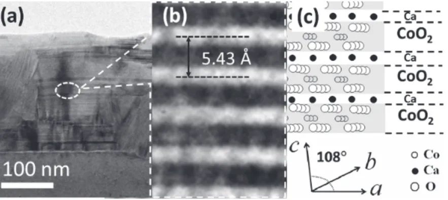
This observation is consistent with the observation by XRD, i.e. the presence of CaO and CoO phases in films deposited. Thermally induced phase transformation of reactive cosputtered CaO-CoO film leads to the formation of the final phase of CaxCoO2. The composition of CaxCoO2 is the Ca0.33CoO2 phase, regardless of the Ca:Co ratio in the film as deposited, i.e. the Ca0.33CoO2 is the most favorable phase in this pathway of thermally induced solid state phase transformation.

Electrical Properties and Interfacial Issues of HfO 2 /Ge MIS Capacitors Characterized by the Thickness of
-V curves and G-Vcharacteristics of the fabricated Al/HfO2/La2O3/Ge MIS capacitors with different ALD cycles of La2O3 passivation layer. a) The control sample; (b) 5 ALD cycles of La2O3 passivation layer;. The This value increases slightly after the insertion of 5 ALD cycles of La2O3 passivation layer, which is consistent with the variation trend of the bumps in C-Vcurves. -frequencyC-Properties measured of the fabricated Al/HfO2/La2O3/Ge MIS capacitors with different ALD cycles of La2O3 passivation layer. a) The control sample; (b) 5 ALD cycles of La2O3 passivation layer;.

New Insights into the Role of Weak Electron–Phonon Coupling in Nanostructured ZnO Thin Films
In this study, we report on the effect of post-annealing on the structural and the optical properties of the magnetron sputtering deposited ZnO thin films. The main focus of this study is to investigate the influence of grain size on the evolution of phonon confinement and the strength of EPC using Raman spectroscopy. The excitation laser power on the sample was ~4 mW with a 1 μm diameter of the laser beam spot.
The value of d~13 nm, which is the width of the nanoplates, remains independent of TA up to 300◦C; above, a drastic increase in grain size can be seen, reaching a saturation value of ~62 nm at TA600◦C. Compared to the ZnO/ALO film, different structural evolution of ZnO from post-annealing of the Zn/ALO film is reflected in the distinct XRD 2-θ scan patterns (Figure S2) as well as the calculated lattice constants and the internal parameter (see the comparison in Table S1 and Figure S3). Compared to bulk ZnO, a redshift from ∼0 to 6 cm-1 was achieved as the grain size decreased from 29 to 2 nm.
Inset of the figure shows the (101) dependence of the spectral width Δω(1LO), where the dashed line is a guide for the eye; (c) Thed(101) dependence of the Raman scattering intensity I1LO, where the solid line is a guide to the eye. The deformation potential and the Fröhlich potential are responsible for the size dependence of the EPC strength. However, in the present set of ZnO films, under resonance conditions, the intensity of the LO phonon increases greatly with the decrease in grain size, and the intensity of the TO phonon is almost insensitive.
The EPC strength derived from the ratio of second-order to first-order Raman scattering intensity shows a linear decreasing behavior with decreasing grain size up to 10 nm, in principle as a result of the Fröhlich interaction.

Notable Enhancement of Phase Transition
Performance and Luminous Transmittance in VO 2
Films via Simple Method of Ar/O Plasma Post-Treatment
Experimental Details
The vacuum chamber was pumped to a base pressure of 6 × 10⁻⁴ Pa, and the substrate temperature was maintained at 480 °C. The flow of Ar and O2 gas was 40 sccm and 2 sccm, respectively, and the working pressure was maintained around 0.5 Pa during deposition. Ar/O plasma irradiation was performed in a vacuum chamber system equipped with a microwave ion source and an operating frequency of 2.45 GHz (Alpha Plasma Q150).
During the plasma irradiation, the flow of Ar and O2 was set as 50 sccm and 100 sccm, respectively, the irradiation power range varied from 350 W to 550 W, and it lasted 30 min for each round. The crystalline phases were identified by X-ray diffractometer (UltimaIV, Rigaku, Tokyo, Japan) with θ-2θ coupled scanning mode (CuKα radiation with a wavelength of 0.15418 nm). The surface roughness was evaluated by Atomic Force Microscopy (AFM) (EasyScan2, Nanosurf, Liestal, Switzerland) with sample size 2μm×2μm.
A field emission scanning electron microscope (Supra 55Sapphire, SIGMA Essential, Jena, Germany) was used to examine the surface morphology of the samples. Horiba Scientific XploRA PLUS Raman spectrum equipped with a 532 nm laser with an output power of 2 mW was used for structural property analysis. The transmission spectra were obtained with a spectrophotometer (Lambda 950, PE, Boston, USA) at 25◦C and 70◦C with a wavelength.
The temperature dependence of the sheet resistances was measured by a four-probe method and the temperature range was adjusted to 25–80◦C for both heating and cooling loops.
Results and Discussion 1. Structure Characteristic
A top view of the model (Figure 1c) shows the binding of clusters occurring in the VO2 interface region. Scanning electron microscope (SEM) images of surface morphologies in VO2 films irradiated with Ar/O plasma at different powers. A comparison between as-deposited VO2 films and 500 W Ar/O plasma irradiated films of typical morphology (Figure 3) highlights the corresponding accumulated changes in the VO2 surface during the irradiation process.
Both quantities increase sharply as the force increases due to the newly formed rod-like clusters, as evident from the SEM images (Figure 2). An SEM micrograph of a vertical section (Figure 3e) reveals that a change in boundary condition is due to recrystallization and surface migration in the underlying region between the top surface and the bulk of the VO2 film with a penetration depth of about 20 nm. The irradiation of the surface causes oxidation because the energy of the coexisting Ar/O ions is high.
A schematic representation of the interaction in a VO2 film during Ar/O plasma irradiation is shown in Figure 3d; a schematic magnification (panel I) shows the crystalline structure of monoclinic VO2(M) in an untreated VO2 film during irradiation. The ratio of the film resistance before and after the phase transition determines the electrical phase transition amplitude ΔA of the film. The power dependence of the thermal hysteresis width ΔH and the phase transition temperature TMI (Fig. 5b) were obtained from standard Gaussian fitting methods by taking the derivative of the logarithmic sheet resistance with respect to the temperature of the VO2 films during heating and cooling cycles.
Thus, the improvement in the electrical phase transition amplitudes can be mostly attributed to details of the stoichiometry as well as the morphology changes in the VO2 surface area [19].

Ultra-Thin Platinum Deposits by Surface-Limited Redox Replacement of Tellurium
Materials and Methods 1. Solutions and Chemicals
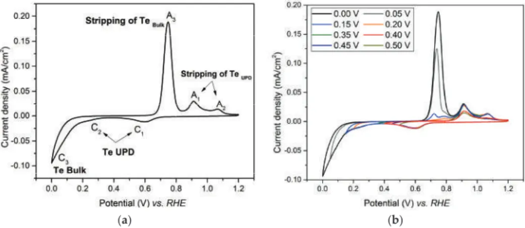
The CV shape is comparable to that recorded during subpotential deposition of Te on gold in sulfuric acid solutions by Suggs and Stickney [30]. Using the electrical charge associated with the reduction of platinum, the Te coverage of the electrode is estimated to be 0.86 ML [40]. Chronoamperometric curve of galvanic replacement of Te with Pt at open circuit voltage (OCV).
RHE only, to avoid the oxidation of the Pt layer obtained by the previous substitutions. One can observe that the intensity of the Te UPD peak increases with the number of substitutions and that its potential (0.35 V vs. RHE) is similar to that determined on a platinum bulk electrode (Section 3.2). The success of the Pt deposition was difficult to determine, due to (i) the ultra-low amount formed on the electrode, which was extremely difficult to characterize, (ii) the impossibility of the Pt deposition on observe the gold rotating disk electrode (RDE) directly.
Figure 7 shows the SEM image and EDS mapping of the layer after 5 cycles of Te deposition and Pt replacement. The electrochemical surface area (ECSA) of the Pt film obtained after 5 replacements was estimated to be 18 m2/g. Red arrows indicate the expected position of Te peaks, indicating the absence of the element in the layer.
Thin-film electrochemical studies of subpotential deposition of cadmium and tellurium on polycrystalline Au, Pt and Cu electrodes.J.
Surface-Limited Electrodeposition of Continuous Platinum Networks on Highly Ordered
Pyrolytic Graphite
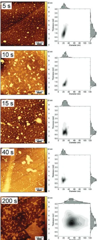
Results and Discussion 1. TM-AFM Analysis
An increase in the degree of interconnection of the Pt nanoplatelets is clearly visible with an increase in deposition time. As shown in Fig. 2a and Table 1, the thickness of the Pt nanoplatelets changed only slightly with deposition time. Most nanoplatelets did not grow more than 4 nm thick, even at longer deposition times (Table 1), with an average between 1.0 and 2.5 nm (equivalent to 5 to 12 Pt monolayers).
This is due to the different conditions of the HOPG surface exposed by cleavage of the C–C stacking [28]. The supporting electrolyte also participates in the Pt growth mechanism and in the determination of the final morphology of the resulting deposit [22,33], its role depending on the concentration and the applied potential. Similar to a previous report [ 38 ], local elemental analysis was performed on three different morphological features (Pt aggregate, Pt nanoplates, and apparently just HOPG) located in a different area of the same sample in Figure 3 .
The EDX spectra of the three zones highlighted in Figure 4 undoubtedly show a Pt signal (Figure 4, inset) also in areas where no Pt nanoplates are visible by STEM. A coupled voltammetric and radiometric (voltradiometric) study of the simultaneous adsorption of hydrogen and anions at platinized platinum electrodes.J. Characterization of the instability of 4-mercaptoaniline-encapsulated platinum nanoparticle solution by combining LB technique and X-ray photoelectron spectroscopy. Appl.
XPS investigation of the early stages of deposition of Ni, Cu and Pt on HOPG.Surf.
Electrodeposition of Two-Dimensional Pt Nanostructures on Highly Oriented Pyrolytic
In this paper, we focus on studying the electrodeposition step in the first cycle of the electrodeposition sequence (200 s). We discuss the effect of the initial electroless deposition of Pt on the formation of 2D nanostructures on HOPG. Preparation of the Pt/HOPG electrode: Full details of the preparation of the Pt electrode on HOPG and [19,29] are reported elsewhere.
At negative potential regions (E < 0.7 V vs. NHE), on Pt, the deposition of Pt from one of the PtClx complexes is expected. The CV for HOPG in the Pt deposition solution is a strong function of the nature of the HOPG surface. The CV of the HOPG exposed to the Pt precursor solution shows the characteristic features for H2evolution, which is consistent with the formation of Pt on the surface.
The Pt deposition occurs preferentially on steps/edges of the HOPG substrate and other defects around the surface. Figure 6C shows that the Pt structures on the HOPG surface become larger NPs, probably due to the reconstruction of the initial Pt nanostructures under the CVs. The corrected current provides an estimate of the amount of Pt deposited under these conditions.
Integration of the Pt deposition flux provides an estimate for the upper limit of Pt deposition corresponding to 40 μg/cm2.


![Knowledge and practice of hand hygiene among dental undergraduates: a cross-sectional study / Khairun Nisa’ Badrul Hisham ... [et al.]](data:image/gif;base64,R0lGODlhAQABAIAAAP///wAAACH5BAEAAAAALAAAAAABAAEAAAICRAEAOw==)