UNLESS OTHERWISE AGREED IN WRITING BY INTEL, THE INTEL PRODUCTS ARE NOT DESIGNED NOR INTENDED FOR ANY APPLICATION IN WHICH THE FAILURE OF THE INTEL PRODUCT MAY RESULT IN A SITUATION WHERE PERSONAL INJURY OR DEATH MAY OCCUR. Designers should not rely on the absence or characteristics of functions or instructions marked as "reserved" or "undefined". Intel retains these for future definitions and assumes no responsibility for conflicts or incompatibilities arising from future changes thereto. Copies of documents bearing an order number referenced in this document or other Intel literature may be obtained by calling or visiting Intel's Web site.
Built-in Specification Clarifications, Specification Changes, and Document Changes from the Intel® IXP43X Product Line of Network Processors Specification Update Change bars indicate areas of change.
Features of the Intel ® IXP43X Product Line of Network Processors
Product Line Features
To determine whether a feature is enabled or not, refer to the Intel® IXP400 Software Programmer's Guide. The Intel® IXP42X family of network processors and Intel® IXP46X family of network processors support PCI operations up to 66 MHz, while the Intel® IXP43X family of products supports PCI operations up to 33 MHz.
Model Specific Features
About This Document
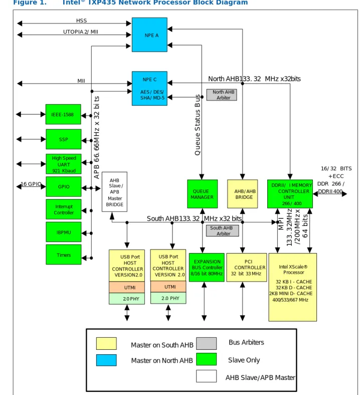
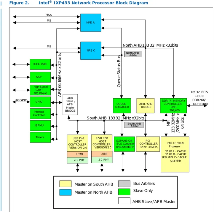
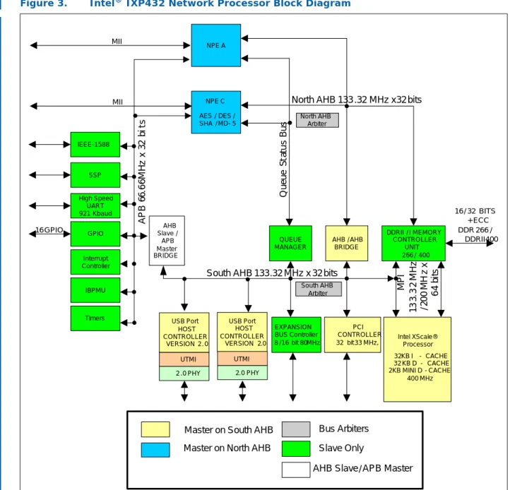
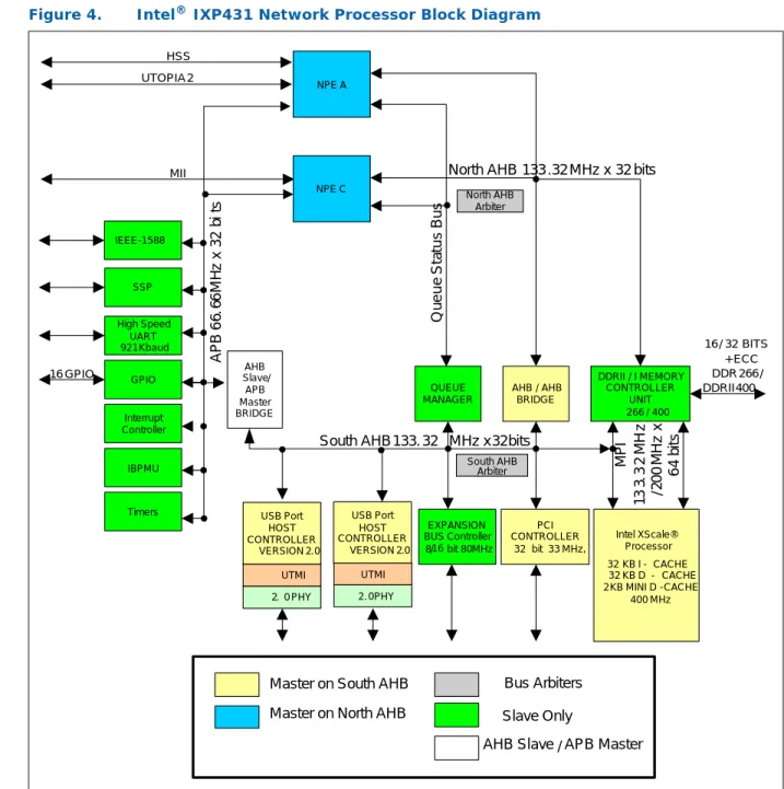
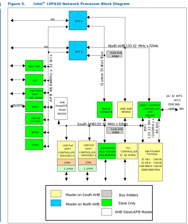
Functional Overview
Key Functional Units
- Network Processor Engines (NPEs)
- Internal Bus
- North AHB
- South AHB
- Memory Port Interface
- APB Bus
- MII Interfaces
- UTOPIA Level 2 Interface
- USB Version 2.0 Host Interface
- PCI Controller
- DDRII/DDRI Memory Controller
- Expansion Interface
- High-Speed Serial Interface
- UART Interface
- GPIO
- Internal Bus Performance Monitoring Unit (IBPMU)
- Interrupt Controller
- Timers
- IEEE-1588 Hardware Assist
- Synchronous Serial Port Interface
- AES/DES/SHA/MD-5
- Queue Manager
Data transfers from the NPE on the North AHB to the South AHB are targeted. The AHB/AHB bridge completes the write on the south AHB when it gains access to the periphery on the south AHB. The AHB/AHB bridge completes the read on the south AHB when it gains access to the edge on the south AHB.
Transfers on the AHB/AHB bridge are considered to be small and infrequent, relative to the traffic passed between the NPEs and the DDRII/DDRI SDRAM on the North AHB.
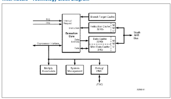
Intel XScale ® Processor
- Super Pipeline
- Branch Target Buffer
- Instruction Memory Management Unit
- Data Memory Management Unit
- Instruction Cache
- Data Cache
- Mini-Data Cache
- Fill Buffer and Pend Buffer
- Write Buffer
- Multiply-Accumulate Coprocessor
- Performance Monitoring Unit
- Debug Unit
Managing the operation of the data cache or minidata cache and the write buffer are categorized as attributes. The attribute bits within the descriptors contained in the ITLB of the IMMU provide some control over the enabled I cache. The attribute bits within the descriptors contained in the DTLB of the DMMU provide significant control over the enabled D cache.
When collation is disabled, memory storage is performed in program order, regardless of the attribute bits within the descriptors located in the DTLB.
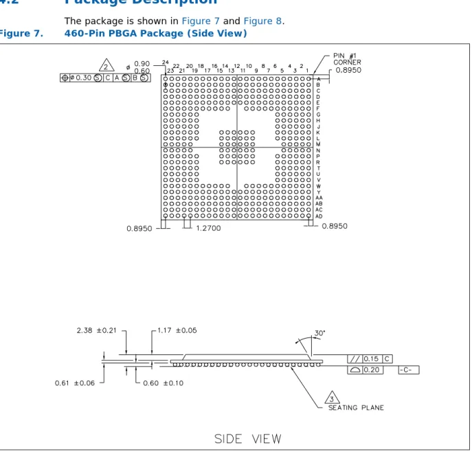
Package Information
Functional Signal Definitions
Pin Types
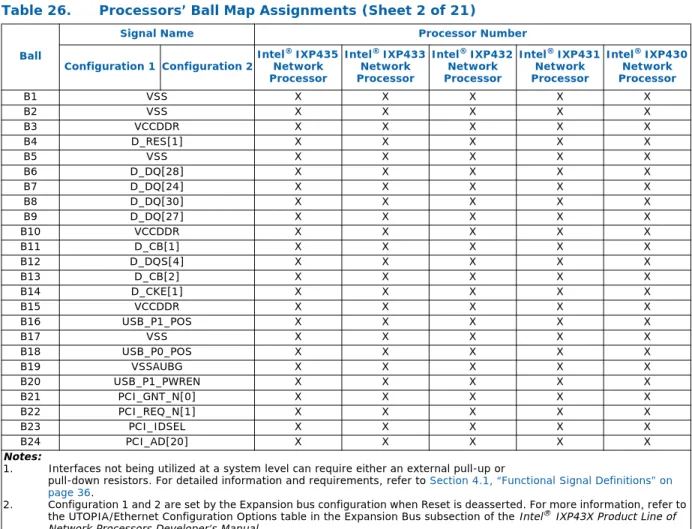
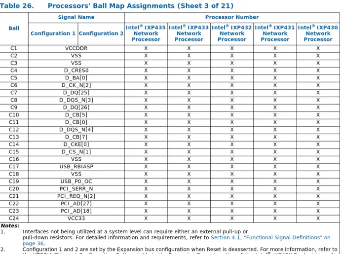
Pin Description Tables
When this interface/signal is enabled and not used in a system design, the interface/signal should be pulled up with a 10-KΩ resistor. When this interface is disabled via the PCI soft fuse and is not used in a system design, it is not required for any connection. When this interface/signal is enabled and not used in a system design, the interface/.
When this interface is disabled by the HSS soft fuse and not used in a system design, it is not required for any connection. When this interface/signal is enabled and not used in a system design, the interface/. signal must be pulled high with a 10KΩ resistor. When the interface/signal is enabled and not used in a system design, it should be pulled high with a 10KΩ resistor.
When the interface/signal is enabled and not used in a system design, the interface/. When this interface is disabled by the UTOPIA Level 2 and/or the NPE-A Ethernet soft fuse and is not used in a system design, it is not required for any connection. EX_CLK Z VI VI VI I Input clock signal is used to sample all expansion interface inputs and clock all expansion interface output.
When this interface/signal is enabled and not used in a system design, the interface/signal should be pulled low with a 10-KΩ resistor. When this interface is disabled via the USB device's soft fuse and is not used in a system design, it is not required for any connection.
Package Description
Signal-Pin Description
Package Thermal Specifications
Electrical Specifications
Absolute Maximum Ratings and Operating Conditions
Warning: Operation beyond the absolute maximum values or operating conditions is not recommended and functional operation is not guaranteed.
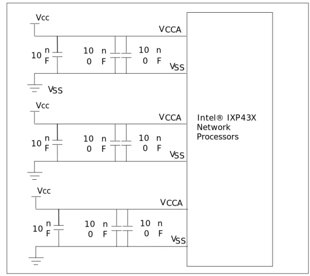
V CCA , V CCP_OSC , V CCAUPLL and V CCAUBG Pin Requirements
- V CCA Requirements
- V CCP_OSC Requirements
- V CCAUPLL Requirements
- V CCAUBG Requirements
A single 170-nF capacitor is connected between the VCCP_OSC pin and the VSS pin on the IXP43X network processors. If 170 nF is an inconvenient size, capacitor values between 150 nF and 200 nF can be used with few adverse effects, provided the effective series resistance of the 200-nF capacitor is below 50 mΩ. To obtain a 200-nF capacitance, a parallel combination of two 100-nF capacitors can be used, as long as the capacitors are placed directly next to each other.
A parallel combination of a 10-nF capacitor for bypass, and a 200-nF capacitor for first-order filter with a cutoff frequency below 30 MHz should be connected to the VCCAUPLL pin of the IXP43X network processors. The ground of both the capacitors should be connected to the nearest VSS supply pin. Both of the capacitors must be located less than 0.5 inch away from the VCCAUPLL pin and the associated VSS pin.
To achieve the capacitance of 200 nF, a parallel combination of two 100 nF capacitors can be used, as long as the capacitors are placed directly next to each other. A parallel combination of a 10 nF capacitor for bypass and a 200 nF capacitor for first-order filter with a cut-off frequency below 30 MHz must be connected to the VCCAUBG pin of the IXP43X network processors. The ground of both capacitors should be connected to the VSSAUBG pin of the IXP43X network processors, which can be connected to the VSS main plane on the board.
DDRII/DDRI RCOMP and Slew Resistances Pin Requirements
For example, when using DDRI SDRAM, DDRIMPCRES is connected to 387Ω and DDRSLWCRES is connected to 845Ω resistor to DDRCRES0.
DDRII OCD Pin Requirements
USB RCOMP and ICOMP Pin Requirements
DC Specifications
- PCI DC Parameters
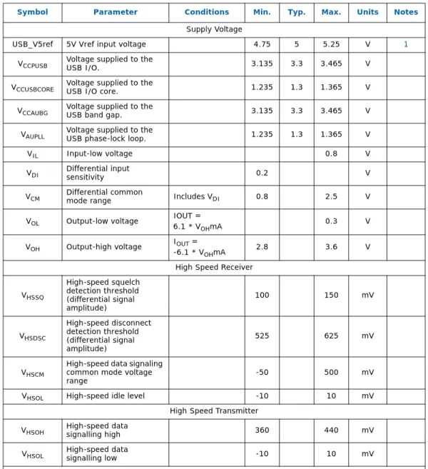
- USB DC Parameters
- UTOPIA Level 2 DC Parameters
- MII DC Parameters
- Management Data Interface (MDI) DC Parameters (MDC, MDIO)
- DDR SDRAM Bus DC Parameters
- Expansion Bus DC Parameters
- High-Speed Serial Interface DC Parameters
- UART DC Parameters
- Serial Peripheral Interface DC parameters
- GPIO DC Parameters
- JTAG DC Parameters
- Reset DC Parameters
- Remaining I/O DC Parameters
When the USB_V5ref pin is tied to 3.3V instead of 5V, the pin cannot carry the short circuit load on the Vbus (5V) and parts are damaged if the Vbus is shorted. The values represented by this voltage parameter are used in a system where the expansion bus connects a single 6pF load placed less than 2 inches away from the IXP43X network processors. This drive power setting should be used to avoid ringing when a minimum load is connected.
The values represented by this voltage parameter are used in a system in which the expansion bus connects four 6pF loads. This drive power setting should be used to prevent ringing when a medium load is connected. The values represented by this voltage parameter are used in a system where the expansion bus connects eight 6pF loads and all components are located less than 6 inches from the IXP43X network processors.
Another example of using this drive power is four 6pF loads operating at 80MHz. This drive power setting should be used to prevent ringing when the maximum load or frequency is used. This is an open drain outlet; the part does not show any drive in this operation, and 2.4V is specified to be achieved by an external board lift.
AC Specifications
Clock Signal Timings
- Processors’ Clock Timings
- PCI Clock Timings
- MII Clock Timings
- UTOPIA Level 2 Clock Timings
- Expansion Bus Clock Timings
Bus Signal Timings
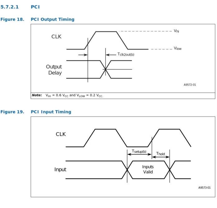
- PCI
- USB Version 2.0 Interface
- UTOPIA Level 2 (33 MHz)
- MII
- MDIO
- DDR SDRAM Bus
- Expansion Bus
- Serial Peripheral Port Interface Timing
- High-Speed, Serial Interface
- JTAG
These values meet the 10-ns setup and hold time requirements required by the MII specification. Talepulse Pulse width of ALE (ADDR is valid at rising edge of ALE) 1 4 Cycles 1, 7 Tale2addrhold Valid address hold time after falling edge of ALE 1 1 Cycles 1, 2, 7 Tdval2valwrt Write data valid before WR_N falling edge 1 4 Cycles 3, 7 Trdsetup Data hold required before rising edge of RD_N 14.7 ns Trdhold Data hold required after rising edge of RD_N 0 ns Trecov Time required between successive accesses when expanding.
Tdholdafterwr Valid data after the rising edge of EXPB_IO_WRITE_N 1 4 Cycles 5, 7 Trdsetup Data valid required before the rising edge of. Tale pulses Pulse width of ALE (ADDR is valid at the rising edge of ALE) 1 4 Cycles 1, 7 Tale2addrhold Valid address hold time from falling edge of ALE 1 1 Cycles 1, 2, 7. Tdholdafterds Valid data after the rising edge of EXP_MOT_DS_N 1 4 cycles 5, 7 Tale2valcs Valid chip selection after the falling edge of ALE 1 4 cycles 7.
Trdhold Data hold required after rising edge of EXP_MOT_DS_N 0 ns Trecov Time required between successive expanding accesses. Trdhold Data hold required after rising edge of EXP_MOT_DS_N 0 ns Trecov Time required between successive accesses to. HSS_RXFRAME00 and HSS_TXFRAME0 can be configured to accept data on the rising or falling edge of the specified reference clock.
Reset
- Cold Reset
- Hardware Warm Reset
- Soft Reset
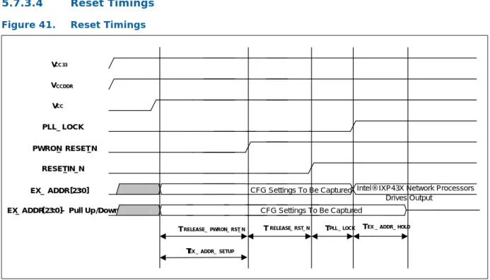
- Reset Timings
Power Sequence
Followed by proper resetting of PWRON_RST_N and RESET_IN_N signals as described in Section 5.7.3.4, “Reset Timings” on page 121. A hardware Warm Reset can only be asserted when PWRON_RST_N is deasserted and the network processor is in a normal operating mode. Since Hardware Warm Reset and Soft Warm Reset are very similar, there must be a way to determine which reset was last performed after recovery.
The minimum time required to hold PWRON_RST_N in the logic 0 state after sustained power has been applied to the IXP43X network processors while using a crystal to drive the processor's system clock. The minimum time required to hold RESET_IN_N at logic 0 after PWRON_RST_N has been released at logic 1. The RESET_IN_N signal is held low when the PWRON_RST_N signal is held low.
Maximum time for PLL_LOCK signal to drive to logic 1 after RESET_IN_N is driven to logic 1 state. Minimum time for the EX_ADDR signals to drive inputs before RESET_IN_N is driven to logic 1 state. Minimum time required to hold the RESET_IN_N signal at logic 0 to cause a warm reset in the IXP43X network processors.
The current must remain stable and the PWRON_RST_N signal must remain stable (logic high) during the process. The expansion bus address is captured as a derivative of the RESET_IN_N signal going high.
Power Dissipation
If applications do not require the use of certain peripherals, or full-speed operation of all peripherals is not required, the power required by the part may be significantly less than the numbers listed in the following table.
Ordering Information