Questions regarding the use of the book should be directed to the Rights and Permissions Department of INTECHOPEN LIMITED ([email protected]). The aforementioned cursory view of the themes encapsulated in Photonic Crystals—A Glimpse of the Current Research Trends highlights some of the current research in the PhC arena that remains of interest.
Introduction
Periodic band-gap structures
At this point, it should be noted that the propagation of light waves in stratified periodic media can be compared to the state of motion of electrons in a periodic potential well [6, 7], if we remember the Kronig-Penney model. This means that such PBG media can be analyzed using the quantum theory of electrons in solids.
Band-gap fibers
This would result in stopping the propagation of electromagnetic waves (through the structure) in certain frequency bands. This is because the basis for the guidance of light waves in dielectric media has a close analogy with the propagation of electrons in solid crystals - the fact that caused tremendous interests in PhC and related research, leading to the development of a wide range of photonic structures for many new applications [8].
Omniguiding fibers
As such, thermal and electrical tuning of the liquid crystals would change the spectral characteristics—a property that can be exploited in the fabrication of tunable PCFs. The number of layers also plays an important role in determining the permitted and prohibited wavelengths, i.e. of band gap conditions.
PhCs with defect
Analytical approach for omniguiding fibers
In the analyzes of omniguiding Bragg fibers, the propagation of Bloch waves is of extreme importance to determine the nature of the propagation. It has further been found that, in the case of omniconducting fibers, the number of allowed and forbidden bands increases with the increase in the difference between the refractive index values of different dielectric layers.
Recent research trends
In addition, the allowed band widths remain larger in the case of stacked layer fibers with greater thickness values [26]. It has also been found in the dispersion characteristics of omniconducting fibers that the width of the allowable range decreases with the increase in k/k0, k and k0 being the wave vector in the medium and that in free space, respectively.
Summary
Also, the effects of incidence angle on band gaps are analyzed and discussed. Such a small shift in the band gaps is related to the different coefficients of thermal expansion of the two materials.
The method of calculation
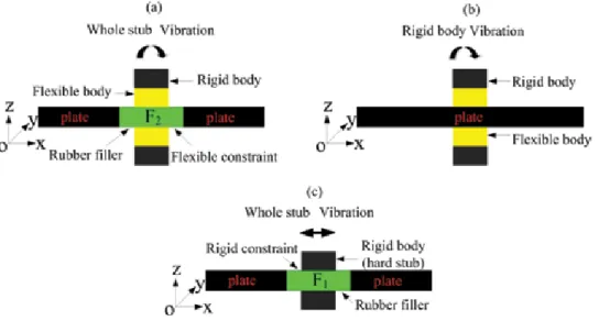
A single-sided sharpened phononic crystal plate [3] consists of a square set of attachments on one side of a homogeneous plate [6]. In other words, extending the bandwidth into the lower frequency region remains a challenging task for a phononic crystal embedded in a metal matrix. TL = 10 log ( α __α oi ) (4) where αo and αi are the output and input acceleration of the phonon crystals embedded in the metal matrix.
The model and the results
The lower frequency complete BG phononic crystals .1 The model of the phononic crystals
TL = 10 log ( __α α oi ) (4) where αo and αi are respectively the output and input accelerations of the metal-matrix embedded phononic crystals. The single unit cell (as shown in Figure 3(b)) is determined by the periodicity of the structure. Band structures of (a) the lower frequency full bandgap metal-matrix embedded PC slab, (b) the transition PC slab and (c) the classical PC slab.
The broad complete BG phononic crystals .1 The model of the phononic crystals
Therefore, the double-sided cone stub has a direct effect on lowering the in-plane band location (53 Hz), and the rubber filler has a direct effect on lowering the out-of-plane band location (59 Hz). Band structures of (a) wide-gap metal matrix embedded phononic crystals, (b) PC transition slab, and (c) classical PC slab. The absolute in-plane bandwidth is increased by a factor of 3.37 compared to a classical phononic-crystal slab [18].
Forming mechanisms of the BGs of the phononic crystals 1 Forming mechanisms of the lower frequency complete BGs
Forming mechanisms of the broad complete BGs
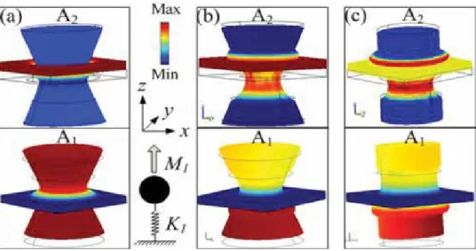
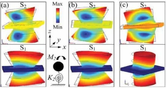
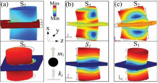
The vector fields of the total displacement of the modes (resonant mode S1, symmetric Lamb mode S2) (a) correspond to Fig. 2(a) , (b) correspond to Fig. 2(b) and (c) correspond to Fig. 2(c) . The vector fields of the total displacement of the modes (resonant mode A1 and antisymmetric Lamb mode A2) (a) correspond to Fig. 4(b) , (b) correspond to Fig. 4(b) and (c) correspond to Fig. 4(c) . Bandgap formation mechanism for the out-of-plane bandgap of (a) transition PC slab, (b) classical PC slab, and (c) wide perfect bandgap phononic crystals embedded in a metal matrix.
The effect of the stubs on the BGs
The effect of the stubs on the lower frequency complete BGs
This causes the spring stiffness ki to increase in the wide full bandgap metal-matrix embedded phononic crystals so that the opening location of the in-plane bandgap is shifted to higher frequencies. One resonator mode is the in-plane analog-rigid mode, in which the entire log vibrates along the in-plane plate. Two raised band gaps overlap to produce a wide full band gap, in which both the out-of-plane and in-plane Lam waves are.
The effect of the stubs on the broad complete BGs
To investigate the effect of single "hard" stumps on the complete phonic bandgaps of the new metal-matrix computers, we studied the effect of the steel stump height on the first complete bandgap. We find that, with the increase of the steel stub height, the location of the first complete band gap shifts to a lower frequency range before moving to a higher frequency range. However, when the steel stub height exceeds 3.5 mm, the location of the band gaps shifts to higher frequencies as the steel stub height increases.
Conclusions
Liquid crystal-based photonic crystal devices
Furthermore, by inserting an LC layer as a defect layer in PCs, the tunable defect modes can be achieved. Larger number of defect modes can be induced by using high refractive index LC or by increasing the thickness of the LC defect layer. Moreover, they demonstrated experimentally and theoretically that the interference of defect modes can be achieved by placing the cell between crossed polarizers.
Aim of this chapter
The wavelengths of the defect modes are shifted by the change in the effective refractive index (neff) [21]. The orthogonal polarization components through the vector sum in the projection direction along the analyzer axis lead to the displacement of the defect modes. With the PC/PSCLC structure, not only is the wavelength of the defect mode switchable between multistable states by voltage pulses, but also the optical intensity of the defect modes can be electrically tuned through switching between different metastable states.
Operation method of liquid crystal-based photonic crystal devices 1 Photonic crystals with a nonchiral nematic liquid crystal
Chiral-tilted homeotropic nematic liquid crystal-based photonic crystal devices
In addition, the intensity of the extraordinary defect modes in the tH state can be tuned by switching between the tH and bH states as an intensity modulator. The blueshift of defect modes for both E and O modes in PC/TN system, and transmission of the PC/TN in the photonic bandgap with three different modes (adapted from [28]). The defect modes of PC/TN for the plain beam are independent of the applied electric field.
Chiral nematic and cholesteric liquid crystal with photonic crystal devices Comparing with the nematic LCs, the configuration of a cholesteric LC (CLC)
The optical intensity of the defect modes is very low in the FC state and the spectra of defect modes in FC are shown in Figure 8. We can see that the blue shift of the H state defect modes is shown and is caused by the reduced effective refractive index in the PC defect layer. In addition, the strength and wavelengths of the defect modes can be tuned by applying voltage and frequency.
Tristable photonic crystal devices with polymer-stabilized cholesteric textures
In addition, the PC/DFCLC in the photonic bandgap with two different sets of defect modes in both P and H states (adapted from [22-24]). In addition, Figure 8 also shows that the hybrid PC/CLC device is in the P state, showing a number of failure modes. The lower transmittance of the defect modes in the PBG is also shown in Figure 10a.
Applications in liquid crystal-based photonic crystals 1 Electrically switchable liquid crystal-based photonic crystals
Liquid crystal-based photonic crystals for pulse compression and signal enhancement in fluorescence applications
In the past, the method is used to reduce the photodamage in the bio-specimen with multiphoton enhanced signal. excitation laser with narrower pulse width. Recently, researchers discovered that multiphoton fluorescence can be amplified with the fluorescence signal, which. Without any dispersion compensators, the PC/LC device may be more suitable for non-photonic researchers.
Photo-manipulated photonic devices based on tristable chiral-tilted homeotropic nematic liquid crystal
The experimental spectra of the PC/TCHN devices were measured under irradiation by controlling both green light and UV light. Based on these optical properties, the PC/TCHN device can be used as tunable optical filters. The PC/TCHN device possesses optical tristability and tunability in wavelength and intensities of the defect modes through photo manipulation.
Conclusions
Defect mode switching in one-dimensional photonic crystal with nematic liquid crystal as defect layer. Defect mode in one-dimensional photonic crystal with in-plane switchable nematic liquid crystal defect layer. Analysis of the defect mode switching response in one-dimensional photonic crystal with a nematic liquid crystal defect layer.
PhC-based mid-infrared gas sensing methods
Mid-infrared light absorption sensing
These methods certainly help to enrich the detection capabilities of PhC in the mid-infrared region. With all this in mind, based on different sensing mechanisms, in the following content, we will detail the recent development of PhC-based gas sensing technologies in the mid-infrared spectrum. Furthermore, most fibers operate below 2 μm, as evidenced by the limited transmission window of silica.
Mid-infrared “refractive index” sensing
In addition, the degree of complexity for the fabrication of PBFs can be lower than PCWs, but still higher compared to the porous silicon PhC devices. In addition, it is possible that the lattice constant of the PhC increases due to the swelling of the gas or vapor. Part of this research is dedicated to investigating the relationship between the value of electric field overlap with the analyte and the sensitivity of the refractive change based sensors.
Mid-infrared electrical conductance sensing
For example, in a porous silicon PhC, when pore regions are filled by a gas, the effective refractive index of the PhC will be increased. As shown in Figure 8, the sensitivity of a PCW sensor directly depends on the percentage of electrical field overlap with the analyte. Detecting an unknown gas using this method can be challenging because the principles of this method are based on changes in the refractive index.
Conclusion
One of the solutions is by realizing photonic crystal (PhC) structures that exhibit high quality factors in a small mode volume, V. It can also be used to recover an electric field component, E(r), from the Maxwell equation given by The Q factor is equal to the ratio of the resonance frequency to the bandwidth of the cavity resonance shown in Figure 2.
It uses a refractive index approach or average refractive index of the sheet—called effective index method (EIM). It is suggested that the different etching depths will give rise to the abrupt change of the effective index, neff, at the.
![Figure 8 shows the relation between the reflectance R versus ωa = 2Pic T ( ω is considered the angular frequency in this relation and c T ¼ c SB ) for P-wave (red dashed lines) and S-wave (black solid lines) [48]](https://thumb-ap.123doks.com/thumbv2/1libvncom/9201493.0/31.765.189.574.665.975/figure-relation-reflectance-versus-considered-angular-frequency-relation.webp)
![Figure 8 shows the relation between the reflectance R versus ωa = 2Pic T ( ω is considered the angular frequency in this relation and c T ¼ c SB ) for P-wave (red dashed lines) and S-wave (black solid lines) [48]](https://thumb-ap.123doks.com/thumbv2/1libvncom/9201493.0/32.765.114.654.765.987/figure-relation-reflectance-versus-considered-angular-frequency-relation.webp)